Blue Morpho Butterfly
A. P. Kunesh(Dated: April 7, 2017)
The Amazonian Blue Morpho Rhetenor’s vibrant blue coloration is an archetype of structural color in the natural world. Drawing inspiration from nature, researchers have attempted to repro-duce the treelike nanostructures for applications in tunable color, security, and gas sensory. Previous work has produced highly periodic structures over small areas; these structures provide the desired color over a small range of viewing angles, but lack the angular independence of the butterfly’s coloration. To remedy this diffractive effect, a Direct Write exposure method is employed to ran-domize the periodicity of spacings between photonic structures. Optimization and implementation of this method yields a variety of heretofore unseen structures, many of which dramatically improve the angle-independence of observed color. Additional finite-difference time-domain simulation gives insight into how each structural parameter affects reflected light. In general, thin, straight trunks with long branches produce optical characteristics most similar to the Morpho.
CONTENTS
Acknowledgments 1
I. Introduction 2
A. Nature and Technology 2
B. Biomimicry of the Blue Morpho Butterfly’s Photonic Structures and Applications 2
C. My Role 3
II. Background and Theory 3
A. Interference and Diffraction 3
1. Thin-Film Interference 3
2. Diffraction 3
B. Previous Work 4
III. Sample Fabrication 4
A. Overview 4
B. Multilayer Fabrication 5
C. Photolithography 5
D. Further Development 5
IV. Implementation of the Direct Write Method 6
A. Overview 6
B. Hardware 7
1. Optics 8
2. Motion control 8
3. Calibration and monitoring 9
C. Software 9
1. Motion control 9
2. Focal monitoring 10
D. DW Exposure Procedure 10
1. Setup 10
2. Calibration 10
3. Initiation 11
4. Maintenance 11
V. Sample Measurement 11
A. The Incident Angle,θ 11
B. The Scattering Angle,φ 11
C. Graphical Data Representation 11
VI. Data, Simulations, and Discussion 12
A. Reference Plots 12
B. Randomizing Periodicity 12
C. Simulations 14
D. Other Avenues Explored via the DW
Method 15
VII. Conclusion and Future Direction 15
References 16
Appendix 17
1. Motion Control Code 17
ACKNOWLEDGMENTS
Many thanks to Cary Tippets and Dr. Rene Lopez, who enabled me to jumpstart my research career over two years ago. Without their guidance and support, this thesis would not exist. Thanks also to my parents, Ben and Racheal Kunesh, who have supported my research endeavors despite only getting fuzzy ideas of my projects. Finally, thanks to the many friends and teachers who have led me to a career in science.
I. INTRODUCTION
A. Nature and Technology
For centuries, man’s fascination with nature has man-ifested itself in our technologies. Daedalus fashioned large, birdlike wings to escape from Crete. More recently, the aerodynamic shape of tropical cowfish became the frame of the Mercedes-Benz Bionic Car1. Nature often
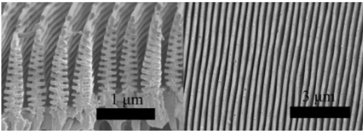
provides insight into novel physical phenomena; explo-ration down these avenues can yield myriad applications. The center of my research has been not a bird or a fish, but a butterfly. The Amazonian Blue Morpho (Figure 1) is characterized by its iridescent blue wings. Like all butterflies, it has a head, a thorax, and an abdomen; scales rest upon its wings. The Blue Morpho is distinct from most butterflies in that its scales are not simply home to a dazzling array of pigments; instead, each scale houses thousands of rows of optical nanostructures. Each of these photonic structures is less than a micron thick and around three microns tall. The structures, having a treelike cross-section, extend for tens or even hundreds of microns along a scale (Figure 2).
FIG. 1. The Blue Morpho. Image credit: Gregory Phillips2.
The function of these structures is to strongly reflect specific wavelengths of light while attenuating others. More simply put, the structures only permit certain col-ors of entering light to leave. The basic mechanics of this process, interference and diffraction, will be examined, but, already, we can make some educated guesses about how these structures perform their optical function.
The branches of the trees are reminiscent of thin films, the optics of which are the subject of introductory physics courses. We might guess, then, that the color of reflected light is heavily dependent on branch thickness. We might
conjecture with similar ease that the intensity of reflected light is related to the density of the tree structures, and could also be affected by the number of branches per tree. The butterfly’s trees present a variety of structural parameters begging exploration.
To the newcomer, this structural color, as it is com-monly called, may seem little more than an interesting rarity. A survey of many beetles, butterflies, and even chameleons3 (see Figure 3) yields, however, that
struc-tural color is not unique to the Blue Morpho.
FIG. 2. SEM images of the profile (left) and length (right) of the Blue Morpho’s optical nanostructures.
FIG. 3. J. Teyssier’s3 discovery that structural color plays a central role in the chameleon’s camouflage.
B. Biomimicry of the Blue Morpho Butterfly’s Photonic Structures and Applications
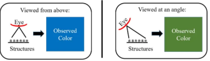
The uniqueness of the Morpho lies in the relative sim-plicity of the structures and the angle-independence of the color. Angle-independence here means that neither the direction of incident light nor the angle of the viewer’s eye relative to the wing surface significantly change the observed color of light. In layman’s terms, the wing looks blue no matter where the sun is and no matter where you are standing. See Figure 4 for a counterexample.
FIG. 4. When an optically angularly dependent material is observed at different angles, perceived color may change.
a particularly interesting application. If the Blue Mor-pho’s nanostructures could be made elastic, it would be easy to control the shape of the trees. By stretching along the rows of structures, we could manipulate the thickness of the branches, allowing for tunable, angle-independent color. “Tunable” here means that the color can be con-trollably and reversibly adjusted.
Much of the initial interest in reproducing the Blue Morpho’s structures stemmed from a drive to produce active camouflage–that is, camouflage that can react to its environment, like the chameleon or the octopus. A screen of pixels cannot do it; tilting the screen of a laptop evidences that. Angle-independent tunable color only ex-ists in the world of nature. By exploiting the Morpho, we hope to bring tunable color into the realm of our control. Other potential applications include security systems and novel gas sensory4. In the first case, a tailored
ma-terial could act as a key to a spectrometric lock. Due to the sophisticated methods required to produce these photonic structures, the key could be very difficult to mimic, especially if its optical data were not known with high precision. A new type of gas sensor, one relying on structural color, is easy to envision. Because the color observed from the butterfly’s wings is, at its simplest, a result of thin-film interference, that color is heavily de-pendent on the gaseous medium surrounding the wings. Though the butterfly only uses its coloration to threaten predators and attract mates, the utility of its photonic structures cannot be overstated.
C. My Role
Previous work has been directed at mimicking the tree profile of the structures at the submicron scale. These structures do produce structural color, but sample pro-duction procedures result in strong angle dependence. That is to say, the observed color is strongly tied to the incident and observing angles. (Again, see Figure 4.) My work’s focus has been to produce angle-independence more closely mimicking the Blue Morpho. Promising re-sults have been achieved by randomizing the spacing be-tween the trees. I played a major role in this random-ization through the implementation, operation, and opti-mization of a novel direct write (DW) fabrication setup. In this paper, I will briefly discuss the background be-fore: detailing sample fabrication in general; expounding
on a novel fabrication method, our DW approach; relay-ing sample measurement techniques; and discussrelay-ing our primary results and conclusions.
II. BACKGROUND AND THEORY
A. Interference and Diffraction
As mentioned briefly, structural color is understood to be a result of interference and diffraction. These phe-nomena have to do with light’s wavelike behavior. The following is a largely qualitative explanation, contextual-ized for the case of the Morpho, and may be passed over by those familiar with the subject. For a slightly more quantitative (but still introductory) treatment, consult a first-year physics text5.
1. Thin-Film Interference
The simplest and most conceptually useful case of in-terference is thin, single-film inin-terference. In this model, a light wave passes from one medium (usually air) into a second medium (in our case, the butterfly’s keratin-based lamella). Each of these materials has its own index of refraction (a physical constant having to do with how much the light’s progression is impeded by the material). These are typically denoted n1 and n2. Now, some of
the light passes directly through the film (or lamella); however, another part of the light reflects, or scatters, off the interface between the air and the film. Another part reflects from the second interface, as the light transitions from the film back into the air.
If the two reflected parts of the light share similar phase (peaks line up with peaks, troughs line up with troughs), we say that there is constructive interference, and the reflected light is intense. If the reflected parts are far out of phase (peaks near troughs), there is destructive interference, and reflected light is dim.
Naturally, if continuous light is shone upon a thin film, the reflected light will be wavelength and angle depen-dent. Light which is well-tuned to the film is reflected, while that which experiences destructive interference is attenuated.
The Blue Morpho’s structures can be thought of as a series of layered thin films, all working together to pro-duce a strongly favored blue light reflection.
2. Diffraction
light sources diffraction gratings. Like thin-film interfer-ence, diffraction is wavelength dependent; the positions of light and dark spots is a result of wavelength.
In the context of the butterfly’s nanostructures, the rows of the structures when viewed from above are rem-iniscent of a diffraction grating. In the case of the ac-tual butterfly, randomness in the spacing between the structures destroys the diffractive effect, resulting in high angle-independence.
B. Previous Work
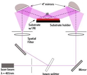
However, previous artificial samples exhibited per-fectly periodic spacings between structures. As a re-sult, these collections of optical structures exhibited high angle-dependence: the desired color, blue, could only be observed over a small sliver of possible angles.
FIG. 5. Old photoresist exposure setup.
This problem arose as a result of previously employed fabrication techniques6 (Figure 5). During
photolithog-raphy (a step which marks out the positions of the trees, covered in greater detail in the Sample Fabrication sec-tion), the spacing was determined using an interferomet-ric setup. In essence, light was manipulated to produce a bunch of perfectly periodic minima and maxima of light. The maxima marked out the position of each structure. As a result, the final tree structures themselves formed a diffraction grating; diffraction begets diffraction.
III. SAMPLE FABRICATION
A. Overview
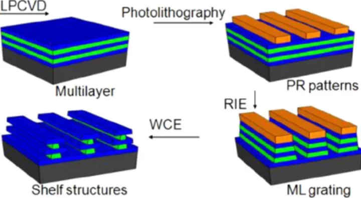
Here I present our general method7 for producing the
Morpho’s photonic structures as it existed before I came into the Lopez laboratory. My innovations were largely relegated to the photoresist exposure step and will be covered later in the work.
Producing photonic structures mimicking the Morpho can be broken down into a series of modular steps: multi-layer production, photolithography, and infilling. Briefly, multilayer production is a process by which several in-terleaving layers of material are deposited onto a wafer; photolithography involves selectively digging down into the newly formed multilayer; and infilling involves filling these newly formed chasms with a desired material, then destroying the multilayer. This process can be readily conceived as the production of a mold followed by the use and destruction of that mold. Figure 6 displays this process graphically, starting with a completed multilayer. The process is described in greater detail in the following subsections.
B. Multilayer Fabrication
We start with a bulk silicon wafer. Ours were 100 mm-diameter mechanical grade wafers with 100 orien-tation, allowing us to cut the wafer into squares at a later point. To begin our fabrication process, we need to produce thin, interleaved materials. These interleaved materials–layers in what we call a multilayer–will be-come the “branches” of our treelike photonic structures. Chemical differences between the two materials will al-low us to chip away at one type of material, leaving the other type unharmed.
To produce these multilayers, we used a special-ized technology: Chemical Vapor Deposition. Specifi-cally, we used Low Pressure Chemical Vapor Deposition (LPCVD). By essentially heating so-called precursor, or source materials, into a gas, we can controllably deposit thin films of metallic substances8.
Using LPCVD, alternating layers of Silicon Dioxide (SiO2) and Silicon Nitride (Si3N4) are deposited to pro-duce our multilayer. Typically, 7 layers of each material were deposited for a total of 14 layers. After a chosen number of layers is deposited, we deposit one final coat: 100 nanometers of chromium. This chromium will serve as a shield for the multilayer later in the process. At this point, the sample is cut into squares roughly 1 cm in side length.
C. Photolithography
The photolithography step involves marking out parts of the sample we wish to remove. We will later destroy the multilayer there, laying the silicon bare. These bare areas will form the trunks of our optical “trees.” In order to understand our photolithographic process, it is first necessary to understand spin-coating and photoresist.
Spin-coating is a process by which a liquid can be de-posited as a uniformly thin film. The basic process is as follows: a sample is secured to a flat platform, usually via vacuum. Deposition of the liquid can occur imme-diately after this step or during the next, which is the spinning phase. After ramping up, the sample is spun, usually at several thousand RPM, flinging away much of the liquid and leaving behind a thin film. In practice, it is important to ensure that minimal dust is present on the sample, as this dust can cause local inequalities in film thickness. It is also important to ensure that the sample’s mass is well-balanced such that it does not fly off during spinning.
Photoresist is the liquid to be spun onto the multi-layer sample, and it is also the multi-layer we use to “mark out” the parts of the multilayer to be destroyed. Pos-itive photoresist is a chemical which, when exposed to a certain wavelength of light for a sufficient length of time, changes its chemical properties and becomes vul-nerable to a developing agent. Areas of the photoresist layer which are not exposed remain in place, while the
developer wipes away exposed photoresist. For negative photoresist, the opposite is true; exposed areas remain in place while unexposed areas develop away. For our fabrication technique, we used positive photoresist. In particular, we used MIC Microposit S1811 resist.
The rest of the process is carried out on a single square multilayer sample. First we spin on a layer of MCC Primer to encourage full adhesion of the photoresist. This layer is spun on at 2,000 RPM for 30 seconds. Af-ter annealing on a hot plate at 115 degrees Celsius for three minutes, the sample is briefly allowed to cool. Now a layer of diluted photoresist is spun on at 7,000 RPM for 40 seconds. (The diluted photoresist is 4 parts S1811 to 1 part Thinner Type P.) The sample is once again al-lowed to anneal at 115 degrees Celsius, this time for one minute.
Now that the photoresist is in place, we can proceed to exposure. There are two conventional exposure methods: masked and direct. In masked methods, a “blueprint” of sorts is placed over the sample, keeping the desired areas dark–masked–while the rest of the sample is exposed to the appropriate wavelength of light. In direct exposure methods, no mask is used, relying on other techniques to direct the light. Our exposure methods are direct; see the following section, Implementation of the Direct Write Method, for greater detail as to how our novel exposure was achieved, or the Previous Work subsection of the Background section for our old interferometric exposure method. The result of the exposure is a set of parallel lines of exposed photoresist, running the full length of the 1 cm sample. You might visualize this set of lines as a cornfield viewed from above. This map will form the row upon row of photonic structures mimicking the scales of the butterfly.
After exposure, the photoresist is selectively removed by application of a developer. In this case, the sample is dipped into Microposit MF-319 developer for a time on the order of a minute, then dipped in two water baths. After drying, etched areas become clearly visible.
D. Further Development
The next nanofabrication tool we need is the Dry Re-active Ion Etcher (DRIE). Basically, a reRe-active ion etcher attacks a surface with directed plasma. The important thing about DRIE for our purposes is that it removes reactive materials, in this case SiO2 and Si3N4, while sparing nonreactive materials, in this case Cr. (This is where the chromium will act as a shield!) Equally im-portant is the directionality of DRIE: as we etch into the multilayer, even layers of multilayer well below our chromium shield retain their integrity.
by photoresist, but by chromium.
Using DRIE, the exposed multilayer is removed at a rate of roughly 70 nm/sec to produce pillars of multi-layer separated by empty space. Again, the empty spaces form the trunks of the nanostructures. Now the sample, complete with its columns of multilayers, is dipped into a 10% hydrofluoric acid (HF) bath. The HF seeps into the spaces between the columns, selectively attacking the SiO2 layers. As the SiO2 recedes toward the center of the columns, we finally achieve treelike structures. This por-tion of the fabricapor-tion is fittingly called the wet etch.
FIG. 7. 3-D view of hard master production process.
We now have a completed “master” mold. (See Figure 7 for a visual summary.) The final step in the process is to fill the mold and destroy it.
We prepare a batch of liquid PFPE (perfluo-ropolyether), a clear polymer which, once it has set, will form our artificial photonic structures. The PFPE is drop-cast onto the sample and degassed via desiccator for half an hour. This degassing ensures that the PFPE fills in not only the trunks, but the far narrower branches. Curing the PFPE is achieved by exposing it to 365 nm light in a nitrogen atmosphere for five minutes.
At this stage, the hardened, clear PFPE is still sur-rounded by multilayer. Bathing the sample in a 48% HF bath for several hours destroys the multilayer, leaving the PFPE nanostructures intact.
Maintaining the integrity of the structures while mov-ing from a completely liquid environment, like the HF bath, to a completely gaseous environment, namely air, is a convoluted process. Surface tension during typical evaporation processes can cause the branches to stick to-gether, destroying the desired optical effects.
After the HF bath, the PFPE replica is transferred to a water bath. Water is gradually replaced by ethanol until the bath is 100% ethanol. Supercritical drying–a process by which the normal evaporation process is bypassed by carefully manipulating temperature and pressure–is the next step. This is done by transferring the sample to a liquid CO2 bath and operating a Tousimis Semidri PVT-3 critical point dryer.
After separating the PFPE from the remaining Si sub-strate and coating the back in carbon black, we have our
product: a colorful polymer replica of the Morpho’s wing (see Figure 8).
FIG. 8. A completed artificial photonic structure sample.
IV. IMPLEMENTATION OF THE DIRECT WRITE METHOD
A. Overview
“Direct Write Method” here means that, instead of producing parallel tree ridges through interference lithog-raphy, each ridge line is engraved directly in photoresist by a mechanically controlled laser setup. In practice, this means that a laser is focused down to a tight spot (<500 nm in diameter) on the sample surface, and then the sam-ple is moved about in such as way as to expose tiny lines of photoresist. Again, these lines form the “cornfield” of tree structures. The width of the lines corresponds to the thickness of the trunks.
While the DW method is conceptually simple (see Fig-ure 9), its implementation proved a challenge. In order for the line size to be controlled, laser focus had to be pre-served across a large distance. While a centimeter may not seem like much at the macro-scale, this distance is four orders of magnitude greater than our focused spot. Because a square centimeter of photonic structures re-quires several thousand lines, motion in one direction had to be very fast. To control the spacing between lines, motion in the other direction had to be very precise. To optimize line thickness, laser power had to be tunable. Finally, we needed software: flexible code to control the exposure and measure the laser focus.
though the resolution of the image would be limited by the laser power. Using the DW method, it was simple to determine a near-optimal set of operating parameters to produce the thinnest, most consistent lines. Our DW method is also fairly low-cost.
The weaknesses of the DW method, as it stands, are increased exposure times and high maintenance. While both issues should be solved by equipment improvements, it takes between 60 and 90 minutes to produce a 1 cm by 1 cm exposure at our closest achievable line spacing. During those 60 to 90 minutes, it is necessary for a user to check (roughly every 15 minutes) that the laser focus has been preserved. If the table has been bumped, a piece of tape has shifted slightly, or a cable has jiggled loose, it can easily mean fifteen minutes of adjustments before exposure can resume.
At several points during my two-and-a-half year tenure in the Nanoscale Optical Materials Lab, pieces of our setup would break, new demands would require new code, or new information would require changes in fabrication procedures. As such, the following represents the most recent incarnation of our DW setup and procedure.
FIG. 9. Idealized direct write method setup.
FIG. 10. Novel direct write method exposure setup.
B. Hardware
FIG. 11. Side view of simplified DW exposure setup.
FIG. 12. Top view of simplified DW exposure setup.
1. Optics
The purpose of the optics system is to produce a highly focused point, or “spot” of consistently intense laser light. This tiny spot is the chisel with which we carve out the lines in our photoresist.
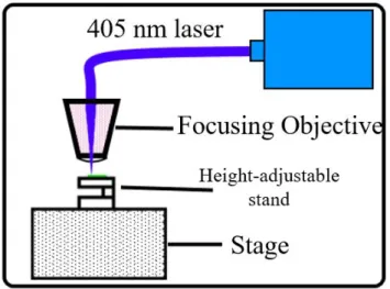
Our optical system consists of an MDL III 405 nm 30 mW laser with a PSU-III-FDA power supply, a Thor Labs FT030 Fiber Optic cable, an E Plan 40x/.65 fo-cusing objective, and a neutral density filter, along with several “adhesive” pieces used to build the tower shown in Figure 10.
The fiber optic cable leads from a focusing setup di-rectly in front of the laser (not pictured) to the tower entry point (top-right, Figure 10). At this point, the neutral density filter may easily be moved into or out of
the path of the beam. This filter is important for use in calibration and focusing, which will be covered later. After being collimated, the laser is directed into the 40x objective. (For those unfamiliar with optics, Figure 11 is a user-friendly image of what is going on here.) Light ex-iting the 40x objective forms a conical shape; the thinnest point of this cone is our desired focus point.
2. Motion control
The purpose of the motion control system is to provide an ultra-stable, mobile platform to which the multilayer sample can be adhered for exposure. The stability con-dition is required such that the focus spot is maintained over the entire surface of the sample. Additionally, the motion of the platform must be fast in one direction–the line-carving direction–to minimize exposure time; in the orthogonal direction–the line position-setting direction– we demand extreme precision and resolution on the order of 10 nanometers. This second demand is made due to the density of structures on the real Blue Morpho’s scales. The motion control system includes a Newport MFA-PPD Nanostepper and ESP3000 controller, a JR 8911 HV hobby servo, a Newport M-426 series linear trans-lation stage, and an Arduino Uno, along with various cables connected to our workstation computer.
To ensure the preservation of laser focus, we required a moving platform which neither rolled nor tilted; it was essential that the stage’s position could be controlled to a resolution well below a micron. After our first stage showed signs of degradation, I applied for funding through the UNC Chancellor’s Science Scholars program and procured the M-426 series stage. This cross-roller bearing stage boasts an angular deviation of less than 150 microradians. Here, angular deviation means “roll” along all axes. Detaching a readily-accessed spring af-forded free motion along the servo axis (see Figure 9). The servo lent us the speed needed in one direction; the nanostepper yielded precision in the other. The 8911 servo was selected due to its high torque and consistent speed. These attributes ensure near-constant line widths. The nanostepper exceeds our requirements, with a reso-lution of 7 nm/step.
The stage is mounted to our lab table. Atop the stage, the nanostepper is held down by several screws. The sample holder, a glass slide, rests on a calibrating stand, which is in turn affixed to the nanostepper. The servo is attached to the stage by a corded wire. The servo is controlled by the Arduino, which is itself controlled by a USB connection to our workstation computer. The nanostepper is controlled by its Newport controller via serial cable; the controller, in turn, receives commands from our workstation computer, again via serial cable.
3. Calibration and monitoring
The purpose of the calibration and monitoring compo-nent is to achieve, monitor, and maintain optimal laser focus. This component is really a lumping together of a variety of smaller, interrelated components.
It consists of a 50/50 beam splitter, a ThorLabs PM120 digital photometer, an IAI CV S3200 digital camera and monitor, an optical tower height adjustment micrometer (Mitutoyo 6031623 and Newport 462 series stage), and a two-screw height-adjustable stand (Newport MMB + ORIEL 14001).
The digital camera, beam splitter, and photometer are used to observe the spot. The beam splitter, housed in-side the optical tower, directs half the incoming light into the photometer, which gives a light intensity readout. The power can be adjusted by turning a micrometer ad-jacent to the laser source, thus blocking some of the beam from entry into the fiber optic cable. The digital camera, which is positioned at the top of the tower, can be used in conjunction with the neutral density filter to directly ob-serve the spot (see Figure 13). The camera also connects to our workstation computer, allowing for quantitative analysis of spot size.
FIG. 13. Direct observation of laser spot.
The tower height adjustment micrometer allows tiny vertical motion of the optical tower. Turning this mi-crometer enables matching the ideal focus to the surface of a sample.
The two-screw height-adjustable stand changes the an-gle of orientation of the sample. Very slight differences in the adhesion of the sample to this stand mean that,
without adjustment, focus is not preserved across the full translational range of the servo or stepper motor. Care-ful calibration of the screws ensures a consistent spot size during exposure.
C. Software
The software necessary to operate the DW exposure setup has two distinct parts: the motion control system, which is controlled through MATLAB R2016b, and the laser focus monitoring system, which is run through Lab-VIEW 8.5.
1. Motion control
The code used to control our DW setup went through several evolutions; for the first few months, coding was done exclusively through Arduino’s default package. This limited the number of allowed lines and constrained the movements of both the servo and nanostepper, so I re-designed the software to operate within a MATLAB framework. The installation of the Arduino servo library was required. With this improvement, it became possible to set any number of arbitrary locations for the servo and the nanostepper. While obtaining a variable, software-controlled servo speed was not possible, this modification drastically improved the versatility of the setup and al-lowed us to optimize our structural parameters at a three-fold rate. Other changes to our rudimentary setup in-cluded added functionality in the form of a digital on/off switch for the laser, improving consistency of line width. At the current time, there are 12 main MATLAB scripts used during operation of the setup. They are (in loose order of importance), startup, runme, reset1, cal-ibrate, locationGen, stepServo, stepStepper, calibrate1, calibrate2, lon, loff, and callimits. The actual text for each of these scripts is included in the Appendix (A1: Motion Control Code), but I will briefly summarize the basic function of each.
startup: Initializes communication with the Arduino (for servo control) and ESP3000 (for nanostepper control). Also calls callimits.
callimits:Sets the range of servo positions during cali-bration.
calibrate:First “shakes” the stage via the servo to en-sure that the sample is secured, then moves slowly within the range set by callimits. Then moves the nanostepper from its home position to a preset dis-tance several times. After this, slow servo move-ment ensues, and so on. For use in setting the height-adjustable stand to preserve focus.
calibrate2: Moves the servo slowly within the range set by callimits. For use in setting the height-adjustable stand to preserve focus.
locationGen: Used to generate locations for an expo-sure run. Here, you can decide: the initial nanos-tepper position; the shape of the random spacing distribution (normal or uniform, and others are easy to implement); the parameters of the random distribution; the average distance between lines; and the number of lines. The system tacks on one final location at 18 mm so that the laser moves be-yond the edge of the sample at the end of a run.
runme: Executes an exposure run. More specifically, runme takes the position elements in the location vector and moves the nanostepper to each location in sequence. At each location, the servo sweeps back and forth. Runme turns the laser on and off such that the sample is only being exposed when the servo is moving in its fastest direction.
reset1: Moves the nanostepper back to its home posi-tion, then sets the servo such that the stage is at the center of its range.
stepServo: Low-level command which moves the servo to a position, desAngle, represented by a value be-tween 0 and 1. This command is essentially a left-over from previous Arduino communication meth-ods, and is not commonly used in equipment oper-ation.
stepStepper: Moves nanostepper to position (in mm) specified by the variable “newLocation.”
lon: Turns laser on (TTL modulation through Arduino pin).
loff: Turns laser off (TTL modulation through Arduino pin).
2. Focal monitoring
By now, it should be obvious that maintaining the fo-cus of the laser on the sample is extremely important. If the laser goes slightly out of focus, the trunks of our nano-optical trees will be inconsistent in thickness, changing the optical properties of the sample. If the laser goes completely out of focus, not enough light reacts with the photoresist, and the end result is the total absence of trees.
For this reason, we took great care to develop methods of monitoring and optimizing our spot size. Cannibaliz-ing the remnants of an old LabVIEW project, we devel-oped a VI which took input from the digital camera and displayed a real-time image of the spot (Figure 13). By measuring the intensity of the light along a line of pixels bisecting the spot, we can quantify the spot size. After
running a series of tests in which we held laser power, line spacing, and development time constant, we determined that the ideal spot size was about 23 pixels. (We have actually had to do this “focus test” many times, but the ideal spot size has always been between 20 and 28 pixels.)
D. DW Exposure Procedure
Though we have come a long way since this project’s origin, the operation of our DW apparatus remains some-thing of an art. While an optimal range of our control parameters (namely laser power, laser spot size, and de-velopment time) has been fairly well defined, consistently tuning these parameters takes patience and developed skill. In my 5 semesters (plus a summer) in the Lopez lab, this activity has taken up the bulk of my time and effort. The following recipe represents a long series of missteps and many, many samples of optimization tests. Once a photoresist-coated multilayer is in hand, there are four basic phases required for exposure: first-sample setup, focus calibration, exposure initiation, and focal maintenance.
1. Setup
Setting up the apparatus takes only a few minutes. Af-ter powering up the laser, the camera, and the rest of the electronic components, MATLAB is launched. Running startup.m brings the servo and nanostepper to life. To save time, I also start the focus observation program in LabVIEW during this step. I set the laser power such that the photometer readout is roughly 200µW. I place the filter in the path of the beam to avoid accidental exposure.
2. Calibration
The sample must be adhered to the height-adjustable stand with detacked double-sided tape. When sticking the sample down, it is best to avoid damaging the center of the sample; personally, I press down on the four corners with a set of curved tweezers.
After the sample is secured and the objective is di-rected at the surface, an initial focusing using the tower micrometer is in order. Once the spot comes into fo-cus, calibrate.m should be run, and the height adjustable stage should be calibrated accordingly. In the event that focus is not maintained along one direction of motion, I might run calibrate1.m or calibrate2.m.
Once I am satisfied with the focus, I can double-check that focus stays the same by moving the sample to its extremes and verifying that spot size stays the same in the LabVIEW program.
resetting, I move the servo such that the laser spot is directed off the sample. Now I remove the filter and bump the power down (usually to 65µW) in preparation for the exposure run proper.
3. Initiation
Given the type of pattern I am interested in producing, I change parameters in locationGen.m. After running lo-cationGen.m, I check the popup display to qualitatively ensure the location vector contains the right values. Af-ter calling runme.m, I double-check my procedure before hitting space bar and proceeding. The servo and nanos-tepper begin their random rhythm.
4. Maintenance
Every 15 minutes or so, I place the filter in the path of the beam and observe the camera screen. If the beam has shifted significantly, I stop the program, rewrite the location vector to contain only the subsequent values, and refocus and/or recalibrate.
V. SAMPLE MEASUREMENT
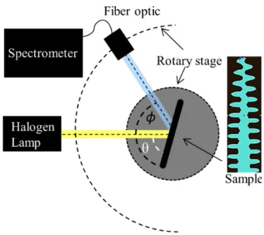
Once a sample has been prepared, its success at mim-icking the butterfly can be difficult to quantify. Our so-lution has been to measure the intensity of reflected light over the visible range at all incident and viewing angles. We achieve this by positioning the sample on a rotat-ing stage. Observation of the light over a 0-to-π range is implemented by an automated spectrometer swiveling about the stage. We call this system our double-angle measurement setup6 (Figure 14).
A. The Incident Angle,θ
After the sample is placed on its rotating stage, colli-mated light, sourced from a continuous-spectrum halogen lamp, is directed at the surface. We call the angle of ro-tation of the stage the incident angle,θ, as it corresponds to the direction the light is coming from given the sam-ple’s frame of reference. At θ=0 degrees, the sample is oriented such the no light hits it; at θ=90 degrees, light is shining directly down on the “tops” of our trees. Fi-nally, at θ=180 degrees, the “sun” has set: the sample has rotated so far that the incident light hits only the far edge of the sample.
B. The Scattering Angle,φ
As light impinges on the sample, the photonic struc-tures disperse and reflect the light at all angles.
Posi-FIG. 14. Double-angle measurement system.
tioning a spectrometer at a variety of angles allows us to gather and decompose optical data by wavelength and the θ-φ angular pair. We call the viewing angle taken by the spectrometer the scattering angle, φ. Note that this angle is measured relative to the stage; in practice, because the halogen lamp is stationary while the spec-trometer and sample rotation, the specspec-trometer moves completely around the double-angle setup. Whenφis 0 or 180 degrees, the spectrometer is “looking” at the trees from the side; it sees a single row, lengthwise. Whenφis 90 degrees, the spectrometer is “looking” directly down at the trees. If this is confusing, take a moment to re-visit Figure 14, paying special attention to anglesθ and φ, marked in black and white at the center of the figure.
C. Graphical Data Representation
Once optical data has been gathered, we can display it graphically in “movies” wherein for each wavelength of impinging light, the incident and scattering angles are held on the x and y axes, respectively9. In each graph,
the intensity of reflected light is given by color. As time proceeds, we can cycle through wavelengths, thus dis-playing data about the intensity of reflection for each wavelength of light at every angle.
VI. DATA, SIMULATIONS, AND DISCUSSION
Hundreds of samples were produced, tens of which were measured. The following represents samples for which the developed area was large enough to measure and the trait of interest is most strikingly visible. Real-data sam-ples (Figures 15-20) highlight the results of randomness in the periodicity of the structures. As expected and desired, introducing randomness drastically reduced the prevalence of diffraction arcs, funneling the intensity into wide-angle nodes instead.
Simulated data (Figures 21-23) explores the effects of nanostructural morphology on optical characteristics. By modeling alterations to the tree symmetry, branch length and taper, and trunk thickness and shape, we gain valu-able guidance for the direction of future experimental research. To summarize, branch asymmetry has little ef-fect; thick trunks act to mute reflected light and spread the nodes; and tapered trunks undesirably move the nodes out to high and low angles. As such, an ideal artificial structure possesses a thin, straight trunk with long, tapered branches.
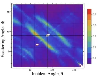
FIG. 15. Double-angle measurement data at 500 nm for an actual Blue Morpho butterfly wing.
A. Reference Plots
In Figure 15, we display the “goal.” This data, taken from an actual Blue Morpho at 500 nm, demonstrates the broad range of angles from which the surface can be observed to have vibrant blue coloration. Graphically, this manifests itself in the broad, spade-shaped nodes toward the center of the image.
Meanwhile, Figure 16 depicts double-angle data at 500 nm for a perfectly periodic artificial sample, produced in our lab using an interferometric setup. My involvement
FIG. 16. Double-angle measurement data at 500 nm for a sample produced using the old interferometric exposure setup.
in the project began with the implementation of the DW method, which, we hoped, would take us from this image to that of the Blue Morpho.
Comparison of Figures 15 and 16 led us to two main goals: the destruction of so-called diffraction arcs, visible as a series of lines roughly parallelingy =−xin Figure 16, and the production of large nodes resembling those of the Morpho. As the following data shows, random-ization of periodicity drastically reduces diffraction arcs and produces nodes.
B. Randomizing Periodicity
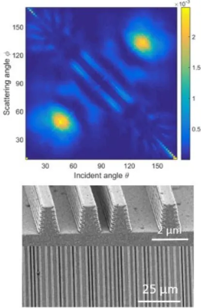
Figure 17 represents my first fabrication achievement. The optical data comes from a sample which was de-signed to be perfectly periodic, with a significantly larger structure spacing than Figure 16. Periodic samples like this were among the first to be produced by the DW ex-posure setup. Note the continued presence of diffraction arcs, those ripple-like lines emanating toward the center. When viewing the physical sample, these blips of intense blue light can be observed on the sample by simply rotat-ing it and watchrotat-ing the colors flash by. Nodes centered around (45, 45) and (135, 135) can be observed. We believe that this is a result of minor randomness in spac-ing due to the imperfection of our setup. Tiny missteps by the nanostepper, coupled with a stage with imperfect straightness, seem to produce just enough randomness for nodes to form.
Below the optical data in Figure 17, see that, com-pared to the actual butterfly’s structures (Figure 2), our structures have lots of empty space between them. As a result, the color of our samples is less intense than that of the Morpho.
FIG. 17. TOP: Double-angle measurement data at 500 nm for an artificial sample with spacing between structures at an exactly periodic 2.5 microns. MID: SEM of profile. BOT: SEM, top-view.
FIG. 18. TOP: Double-angle measurement data at 500 nm for an artificial sample with spacing between structures as a uniformly random variable distributed from 2.0 to 3.0 mi-crons. MID: SEM of profile. BOT: SEM, top-view.
was allowed to vary by .5 microns. Specifically, the dis-tance between subsequent trees was chosen using a uni-form distribution with bounds at 2.0 and 3.0 microns.
Comparison of Figure 18 with Figure 17 yields that the introduction of randomness nearly decimates diffraction
arcs. At the center of the graph in Figure 18, however, diffraction arcs can still be observed running to the cor-ners.
SEM images of this first random sample show tree spacings very similar to the periodic sample; only the occasional outlier allows the human eye to distinguish between the two. This random distribution of spacings became our “default” test spacing any time we wished to change a structural or procedural parameter.
FIG. 19. TOP: Double-angle measurement data at 500 nm for an artificial sample with spacing between structures as a uniformly random variable distributed from 1.5 to 3.5 mi-crons. MID: SEM of profile. BOT: SEM, top-view.
Interested in further testing the effects of randomized spacing on unwanted diffraction arcs, we increased the range of spacing variation (Figure 19). This sample, pro-duced using a uniform distribution with bounds at 1.5 and 3.5 microns, demonstrated continued reduction of well-defined diffraction arcs and increased the spread of the nodes. When viewed using SEM, the randomness in spacing is immediately visible.
FIG. 20. TOP: Double-angle measurement data at 500 nm for an artificial sample with spacing between structures as a uniformly random variable distributed from 1.0 to 4.0 mi-crons. MID: SEM of profile. BOT: SEM, top-view.
C. Simulations
Casual comparison of the optical data from these arti-ficial structures to that of the actual Morpho shows that there is still much to be desired. While randomness in spacing produces nodes and attenuates diffraction arcs, the size and location of the nodes is dramatically differ-ent. In the hopes of pinning down desirable structural parameters, we reached out to a previous group member, Eugene Donev, to simulate a variety of tree morpholo-gies. Simulations were performed using FDTD Solutions of Lumerical Solutions, Inc. The main parameters we varied were: branch symmetry; branch length; vertical branch taper; vertical trunk taper; and trunk thickness. In general, thin, straight trunks with long branches pro-duce the most desirable optical characteristics. We con-tinue to use these simulations as a foundation upon which to build new fabrication procedures.
FIG. 21. LEFT: Simulated optical data for our exact tree profile. MIDDLE: Simulated optical data for a symmetric (IE reflected, right to left) tree profile. RIGHT: Simulated optical data for a tree profile of similar shape, but with perfectly rectangular branches.
One of the features of the Morpho’s structures is left-right asymmetry. The butterfly’s lamellae zigzag from branch to branch, whereas our multilayer fabrication is restricted to symmetry: perfectly stacked branches. Though through clever prepatterning we can get the oc-casional asymmetric structure, we have had difficulty scaling up. Fortunately, as Figure 21 shows, asymme-try does little but slightly redistribute intensity from one node to another. Figure 21 also shows that produc-ing perfectly rectangular branches would only slightly increase the size of the nodes. Note the locations of the nodes; in contrast with the butterfly, our nodes are far from the center of the graph. While far less angle-dependent than previous artificial samples, ours are best viewed at low and high angles.
FIG. 22. LEFT: FDTD simulation of a thick-trunk structure. RIGHT: FDTD simulation of a thin-trunk structure.
One of the greatest weaknesses of our DW setup is the width of our exposure lines. This width translates to thick trunks. Taking cues from the Morpho’s thin trunks, we simulated two idealized structures with equal-length branches but different-thickness trunks (Figure 22). Note that the trunks of each structure are straight. The widths of the trunks are consistent throughout. While the thick trunk seems to spread the light more effectively, the over-all node intensity and shape is undesirable. Compared to Figure 21, these straight-trunk simulations have nodes much closer to the center, like the Morpho. Generating artificial samples with straight, thin trunks should pro-duce angle-independence at intermediate angles (“head on”).
FIG. 23. TOP: FDTD simulation of a structure with ta-pered branches and a straight, thin trunk. BOTTOM: Real structure with tapered branches and a nearly-straight, thicker trunk.
D. Other Avenues Explored via the DW Method
In an attempt to mimic yet one more feature of the Blue Morpho, we implemented a light chopper into our exposure setup. A chopper is a lot like a stand fan: ro-tating blades selectively cut off, or chop, the laser light. The Morpho’s structures do not go on for thousands of microns; instead, the ridges start and stop, sometimes flowing into each other. By setting the chopper to re-move 50% of the light at roughly 300 Hz, we produced the structures pictured in Figure 24. Note that when we employ both randomness in spacing and the chop-per, diffraction arcs are almost invisible while nodes are clearly present. Due to the low intensity of chopper sam-ples, we tabled this avenue of exploration; however, by introducing randomness on several levels, we achieved a more desirable result.
We also tried using different random distributions to sample our nanostructure spacings. After concluding that the uniform distribution tended to yield the broadest nodes, we shifted to primarily producing those samples.
VII. CONCLUSION AND FUTURE DIRECTION
Intrigued by the applications of structural color, re-searchers turned to the Blue Morpho butterfly for inspira-tion. This butterfly, garbed in the brilliance of millions of tiny, clear nanostructures, promises to deliver novel tech-nology in active camouflage, gas sensory, and security. Our loftiest goal is to produce tunable color by casting these nanostructures in an easily-manipulated elastomer; in accordance with thin-film interference, the color of re-flected light could be controllably and reversibly shifted by changing the thickness of the structures’s lamellae, or branches.
At the beginning of my involvement in the project, clear structures mimicking those of the Morpho had been produced. However, byproducts of an interferometric photoresist exposure method resulted in unwanted op-tical angle-dependence in the finished product.
FIG. 24. TOP: Double-angle measurement data at 500 nm for an artificial sample with spacing between structures as a uniformly random variable distributed from 2.0 to 3.0 mi-crons. For this particular sample, a chopper was employed to expose only short segments over the course of each line. MID: SEM of profile. BOT: SEM, top-view.
Great strides have been made in increasing the angle-independence and physical area of photonic structure samples. By implementing a direct write exposure setup, it became possible to produce rows of photonic structures for which spacing was randomized, aperiodic. Through a mixture of experimentation and simulation, we have gathered insight into what structural factors influence angle-independence.
While our DW setup has proven itself capable of pro-ducing angle-independent samples, there is still much to be done. To increase the color intensity, a greater density of structures is required. This mandates a tighter laser fo-cus and a fine-tuning of etching methods. A tighter laser focus is necessary to reduce the maximum thickness of a given tree trunk. A fine-tuning of etching methods to re-duce tapering of the trunk will also allowed for increased structural density.
Reducing trunk taper and thickness, along with in-creasing mean branch length, is a subject of current lab research. In optimizing these parameters, we hope to further increase angle-independence and tailor the op-tical characteristics of artificial samples to more closely match the butterfly. In particular, we hope to bring the nodes closer together and broaden their extent.
hopeful that future experimentation and discovery will make tunable, angle-independent color a reality.
1
B. de Pastino, National Geographic (2005).
2 G. Phillips, “Photograph of a Blue Morpho butterfly (Mor-pho menelaus),” (2003).
3
J. Teyssier, Nat. Commun. , 6308 (2015).
4 W. Zhang, J. Gu, Q. Liu, H. Su, T. Fan, and D. Zhang, Physical Chemistry Chemical Physics (2014), 10.1039/C4CP01513D.
5
D. Haliday, R. Resnick, and J. Walker, Fundamentals of Physics, 10th ed. (Wiley, Hoboken, NJ, 2013).
6
C. A. Tippets, Y. Fu, A. M. Jackson, E. Donev, and R. Lopez, Journal of Optics18(2016).
7 M. Aryal, D.-H. Ko, J. R. Tumbleston, A. Gadisa, E. T. Samulski, and R. Lopez, Journal of Vacuum Science & Technology B: Microelectronics and Nanometer Structures 30, 061802 (2012).
8
C. C. Wang, K. H. Zaininger, and M. T. Duffy,RCA Labs, Tech. Rep. (Pinceton, NJ, 1970).
APPENDIX
1. Motion Control Code
startup.m
a = arduino(’COM3’, ’uno’, ’Libraries’, ’Servo’); s = servo(a, ’D11’);
serialCom=serial(’COM4’); set(serialCom,’BaudRate’,19200); set(serialCom,’DataBits’,8); set(serialCom,’Parity’,’none’); set(serialCom,’StopBits’,1); set(serialCom,’FlowControl’,’hardware’); set(serialCom,’Terminator’,’CR’); fopen(serialCom); callimits; firsttime=1; runme.m numLines=numel(location); fprintf(’FINAL CHECK...’) pause() for count=1:numLines newLocation=location(count); lon; pause(.05) stepStepper; writePosition(s,.28); pause(.25); loff; pause(.05) writePosition(s,.72); pause(.25); end reset1.m newLocation=0; stepStepper; writePosition(s,.5); calibrate.m servoPos=readPosition(s); pauseamt=.002; strokeSize=.005; callimits; if firsttime==1 for countah=1:10 writePosition(s,maxServo); pause(.4) writePosition(s,minServo); pause(.4) end firsttime=0; else end for calibCount=1:2 for countah=1:20 while servoPos¡maxServo writePosition(s,servoPos+strokeSize) pause(pauseamt) servoPos=servoPos+strokeSize; end while(servoPos¿minServo) writePosition(s,servoPos-strokeSize) pause(pauseamt) servoPos=servoPos-strokeSize; end end writePosition(s,.5)
location=[0 10 0 10 0 10 0 10]; for(j=1:numel(location)) newLocation=location(j); stepStepper end end for countah=1:5 while servoPos¡maxServo writePosition(s,servoPos+strokeSize) pause(pauseamt) servoPos=servoPos+strokeSize; end while(servoPos¿minServo) writePosition(s,servoPos-strokeSize) pause(pauseamt) servoPos=servoPos-strokeSize; end end writePosition(s,.5) location=[0 10 0]; for(j=1:numel(location)) newLocation=location(j); stepStepper end locationGen.m clear location avg=.0025; normStDev=.0005; unifBound=.001; numLines=5000; location(1)=0;
%Moving on to the normal lines
%location(end+1)=location(end)+expSpace; %normRNs=(randn(1,100)*normStDev+avg) %negCount=0; %for count=1:100 %if normRNs(count)¡0 % normRNs(count)=0; % else % negCount=negCount+1; % end % location(end+1)=location(end)+normRNs(count); %end
unifRNs=(rand(1,numLines)*unifBound-1/2*unifBound)+avg;
for count=1:numLines
glhf=location(end)+unifRNs(count); location(end+1)=glhf;
end
location(end+1)=18; plot(location)
stepServo.m
writePosition(s,desAngle);
stepStepper.m
command=[’1’, ’PA’ ,num2str(newLocation)]; fprintf(serialCom,command);
pause(.01)
fprintf(serialCom,’1TP’); currentLoc=fscanf(serialCom,’
while (abs(currentLoc-newLocation)¿.00006) %.6 micron resolution
fprintf(serialCom,’1TP’); pause(.01)
currentLoc=fscanf(serialCom,’ pause(.01)
end
calibrate1.m
location=[0 5 0 5 0 5 0 5 0 5 0 5 0] for(j=1:numel(location))
newLocation=location(j); stepStepper
end
calibrate2.m
servoPos=readPosition(s); pauseamt=.002;
strokeSize=.005; if firsttime==1 for countah=1:10
writePosition(s,maxServo); pause(.4)
writePosition(s,minServo); pause(.4)
end
firsttime=0; else
end
for countah=1:100 while servoPos¡maxServo
writePosition(s,servoPos+strokeSize) pause(pauseamt)
servoPos=servoPos+strokeSize; end
while(servoPos¿minServo)
writePosition(s,servoPos-strokeSize) pause(pauseamt)
servoPos=servoPos-strokeSize;
end end
lon.m
writeDigitalPin(a, ’D13’, 1);
loff.m
writeDigitalPin(a, ’D13’, 0);
callimits.m