THE MICROIONIZER – A SOLID STATE ION SOURCE FOR HIGH PRESSURE MASS SPECTROMETRY
Craig A. Cavanaugh
A dissertation submitted to the faculty at the University of North Carolina at Chapel Hill in partial fulfillment of the requirements of Doctor of Philosophy in the Department of
Applied Physical Sciences.
Chapel Hill 2016
ABSTRACT
Craig A. Cavanaugh: The Microionizer – A Solid State Ion Source for High Pressure Mass Spectrometry
(Under the direction of J. Michael Ramsey)
This work describes the development of a novel, microfabricated solid-state ionization source (a “microionizer”) for use with high pressure mass spectrometry (HPMS). HPMS is intended for miniature, low-cost, portable instrumentation. As such, the microionizer is designed as a small, low-power ion source compatible with the 1 Torr air-based environment of HPMS. The microionizer is a field effect device based upon silicon-on-insulator
technology that functions as a dual-source, producing field emission for internal electron impact ionization (EI) and external field ionization.
External ion injection into the miniature cylindrical ion trap (mCIT) was performed in helium, nitrogen, or air buffer gases at 1 Torr using traditional ion sources (thermionic emitter and glow discharge) for proof-of-concept experiments. Further studies in helium and air examined the effects of pressure, ion kinetic energy, and ion trap potential well depth changes with drive radiofrequency (RF) signal frequency and amplitude. Results indicated that mass spectral signal intensity can be maximized at pressures ranging from 10 to
1000 mTorr by tuning ion kinetic energy between 20 to 250 eV and increasing potential well depth aids external ion injection.
limited the microionizer lifetime and prevented field strengths necessary for field ionization. Generations two through nine encompassed processing variations of device fabrication procedures, development of robust electrical contacts, and microionizer device incorporation into the ion trap electrode stack, leading to improved microionizer signal intensity and low power (< 1 mW average power) consumption.
The ninth generation microionizer demonstrated operation as both a field emission and field ionization source in air buffer gas at 1 Torr. Electric field strengths for field emission were near 1 MV/cm, while field ionization required greater than 1.8 MV/cm. The
ACKNOWLEDGEMENTS
TABLE OF CONTENTS
LIST OF TABLES ... xii
LIST OF FIGURES ... xiii
LIST OF ABBREVIATIONS AND SYMBOLS ... xviii
CHAPTER 1: INTRODUCTION – HIGH PRESSURE MASS SPECTROMETRY AND THE MICROIONIZER ... 1
1.1 Motivation for Handheld Mass Spectrometry... 1
1.2 Current Technology in Miniaturized Mass Spectrometers ... 3
1.2.1 Miniaturized Mass Analyzers ... 4
1.2.2 Portable Ion Trap Mass Spectrometers ... 4
1.3 High Pressure Mass Analysis... 7
1.3.1 System Components for HPMS – Mass Analyzer ... 9
1.3.2 System Components for HPMS – Ion Detector ... 11
1.3.3 System Components for HPMS – Ion Source... 12
1.4 Advanced Ion Sources ... 13
1.4.1 Internal vs. External Ionization ... 15
1.4.2 Ionization Methods for High Volatility Analytes ... 16
1.4.3 Field Effect Devices for Mass Spectrometry ... 18
1.5 Field Effect Applications and Theory ... 20
1.5.3 Pressure Tolerance and Lifetime ... 24
1.5.4 Fabrication ... 25
1.6 Solid State Microionizer ... 26
1.6.1 Design and Operation ... 26
1.6.2 Examples of Similar FEDs... 28
1.6.3 Advantages of the Microionizer... 29
1.7 Objectives and Roadmap ... 30
1.8 Figures... 31
1.9 REFERENCES ... 37
CHAPTER 2: THERMIONIC AND GLOW DISCHARGE SOURCES FOR HPMS APPLICATIONS ... 53
2.1 Introduction ... 53
2.2 Experimental Section ... 55
2.3 Results and Discussion ... 59
2.4 Conclusions ... 68
2.5 Figures... 70
2.6 REFERENCES ... Error! Bookmark not defined. CHAPTER 3: INITIAL MICROIONIZER DEVELOPMENT ... 83
3.1 Introduction ... 83
3.2 Experimental ... 87
3.3 Results and Discussion ... 88
3.3.1 1st Generation Microionizer as a Field Emission Source ... 89
3.3.3 Mass Spectrometry in Air Buffer Gas ... 92
3.3.4 1st Generation Microionizer Characterization ... 93
3.4 Conclusions ... 95
3.5 Figures... 97
3.6 REFERENCES ... Error! Bookmark not defined. CHAPTER 4: MICROIONIZER FABRICATION AND DEVELOPMENT ... 110
4.1 Introduction ... 110
4.2 Fabrication ... 113
4.2.1 Early Development – Generations 2 to 6 ... 115
4.2.2 Optimization – Generations 7 through 8 ... 116
4.2.3 Final Process – Generation 9 ... 116
4.3 Experimental ... 117
4.3.1 HPMS Updates... 117
4.3.2 Microionizer Operation ... 118
4.3.3 Characterization and Testing ... 120
4.4 Results and Discussion ... 121
4.4.1 Fabrication and Leakage Current ... 121
4.4.2 Field Emission Mode Operation ... 126
4.4.3 Positive Mode Operation ... 130
4.5 Conclusions ... 132
5.1 Introduction ... 157
5.2 Experimental ... 159
5.3 Results and Discussion ... 162
5.3.1 Field Emission HPMS Characterization ... 162
5.3.2 Field Ionization HPMS Characterization ... 166
5.3.3 Modes of Failure ... 174
5.4 Conclusions ... 175
5.5 Figures... 176
5.6 REFERENCES ... Error! Bookmark not defined. CHAPTER 6: CONCLUSIONS AND FUTURE WORK ... 189
6.1 Conclusions ... 189
6.2 Future Work ... 192
6.2.1 Microionizer as Atmospheric Inlet ... 193
6.2.2 Microionizer as Ion Trap Endcap ... 194
6.2.3 Further Microionizer Development ... 195
6.3 Applications Beyond HPMS ... 196
6.4 Figures... 197
6.5 REFERENCES ... Error! Bookmark not defined. APPENDIX 1: LIST OF MICROFABRICATION TECHNIQUES, TOOLS, AND GENERAL RESOURCES ... 201
A1.1 Tools and Techniques Used During Fabrication Development ... 201
A1.2 Notes and Resources ... 202
A1.2.2 Cleaning and Wet Etches ... 202
A1.2.3 AZ-9260 Guidelines ... 204
A1.2.4 Thin Metallic Films ... 205
LIST OF TABLES
Table 4.1: Substrate characteristics for each generation of microionizer. ... 136
Table 4.2: Final process flow from wafer to microionizer. ... 137
Table 4.3: List of the substrates used for Gen 9 devices. ... 147
LIST OF FIGURES
Figure 1.1: Cross sectional schematics of quadrupole and cylindrical ion traps showing critical dimensions and equipotential lines...31
Figure 1.2: Stability diagram for a quadrupole ion trap, where mass
selective instability mode is highlighted in red...32
Figure 1.3: Examples of conventional ionization sources including a
thermionic emitter as well as glow discharge. ...33
Figure 1.4: Examples of field effect devices which have been coupled with mass spectrometers. ...34
Figure 1.5: A cross-sectional schematic of the microionizer including the high-field region, operational voltages, and layering of the SOI substrate. ...35
Figure 1.6: First generation microionizer layout with an SEM magnification of an array of active features as well as a single 20 µm via. ...36
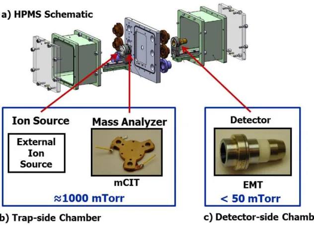
Figure 2.1: a) An exploded rendering of the differentially pumped mass spectrometer (HPMS). ...70
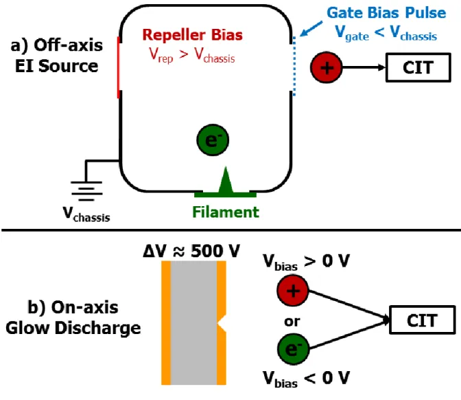
Figure 2.2: a) Schematics of external ion sources including the off-axis
electron impact ionization source and on-axis glow discharge source. ...71
Figure 2.3: Normalized mass spectra of mesitylene generated using the off-axis EI source in helium and nitrogen buffer gases at 1030 and 405 mTorr, respectively. ...72
Figure 2.4: Integrated mass spectral signal of mesitylene as a function of pressure in helium and nitrogen buffer gases recorded using the off-axis EI source. ...73
Figure 2.6: Mass spectra of mesitylene in air buffer gas at 1015, 630, and 375 mTorr taken with the on-axis ion source with energies
between 0 and 150 eV ...75
Figure 2.7: Mesitylene mass spectra recorded at 1015 mTorr in air buffer gas with on-axis glow discharge in both ion and electron modes. ...76
Figure 2.8: Drive RF amplitude effects on ion injection at 1 Torr with the mCIT using mesitylene and on-axis glow discharge. ...77
Figure 2.9: Drive RF frequency effects on ion injection at 1 Torr with the mCIT using on-axis glow discharge. ...78
Figure 3.1: Optical and SEM images of the microionizer, including a cross
sectional view highlighting the layers of the SOI substrate. ...97
Figure 3.2: Image of the microionizer mount used at UNC as well as a
schematic of the device showing the operation voltages. ...98
Figure 3.3: Summary of ORNL microionizer results for a single trench device operated at various bias voltages of various analytes in helium buffer gas. ...99
Figure 3.4: Mass spectra of xenon in helium buffer gas at 4.9 mTorr and 960 mTorr recorded with the first microionizer. ...100
Figure 3.5: Mass spectrum of mesitylene in 510 mTorr of room air recorded with the first generation microionizer. ...101
Figure 3.6: Integrated mass spectral signal intensity of xenon in helium buffer gas as a function of microionizer electric field strength. ...102
Figure 3.7: Integrated mass spectral signal intensity of xenon in helium buffer gas as a function of microionizer bias potential. ...103
Figure 4.2: Optical image of representative microionizers from each generation of development. ...135
Figure 4.3: Optical images of each version of the 9th generation microionizer as well as a PCB-mounted and wire-bonded microionizer. ...138
Figure 4.4: Evolution of the HPMS, showing the decrease in mCIT size as well as the vacuum chamber. ...139
Figure 4.5: Comparison of the output pulse voltage of the PVA 3354n optical relay vs. the High-Voltage Switch. ...140
Figure 4.6: Evolution of the microionizer PCB mount. ...141
Figure 4.7: Cross-sectional SEM of Gen 9.3 device, the bias and pulse voltages are schematically shown as well as a high-resolution SEM of field enhancement sites. ...142
Figure 4.8: Schematic of the microionizer test setup used to measure field emission and ionization intensity. ...143
Figure 4.9: Representative current draws as a function of electric field
strength for three generations of microionizers: Gen 5; Gen 8; and Gen 9. ...144
Figure 4.10: Images of Gen 8 wire bonds utilizing 1 mil diameter aluminum wire and titanium/copper bond pads and Gen 9 wire bonds consisting of 0.5 x 1.5 mil2 gold ribbon and titanium/palladium/gold bond pads. ...145
Figure 4.11: Image of processed Gen 9.6 wafer and summary of wafer-level
failure analysis. ...146
Figure 4.12: Field emission signal intensity as a function of electric field strength for Gen 9.1, 9.3, 9.5, and 9.6 microionizers as well as a
Fowler-Nordheim re-plot of the results. ...148
Figure 4.14: Field emission signal intensity as a function of a gating potential at 1 Torr for a Gen 9.5 microionizer as well as average current consumption during field emission for Gen 9.1, 9.3, 9.5, and 9.6 microionizer. ...150
Figure 4.15: Field ionization signal intensity as a function of electric field strength for Gen 9.1, 9.3, 9.5, and 9.6 as well as field ionization signal intensity versus gating potential for a Gen 9.5
microionizer. ...151
Figure 5.1: Cross sectional schematic of the mini-chamber HPMS with a trap mounted microionizer. ...176
Figure 5.2: The mini-chamber HPMS adapted to work with the trap-mounted
microionizer. ...177
Figure 5.3: High pressure mass spectrum of o-xylene at 1.0 Torr air buffer gas using the microionizer in field emission mode. ...178
Figure 5.4: The lifetime of a Gen 9.1 microionizer operated in field emission mode in air buffer gas. ...179
Figure 5.5: Mass spectra of several VOCs (mesitylene; toluene; benzene; and aniline, methylaniline, and dimethylaniline) acquired in field
ionization mode at 0.93 Torr of room air. ...180
Figure 5.6: Overlay of mesitylene mass spectra (as well as ionization pulse) in air buffer gas with similar signal intensity recorded in field emission and positive modes. ...181
Figure 5.7: Mass spectra of a dimethylaniline and benzene mixture using field ionization with increasing field strengths of 1.17 MV/cm; 1.53 MV/cm; 1.67 MV/cm; and 1.80 MV/cm. ...182
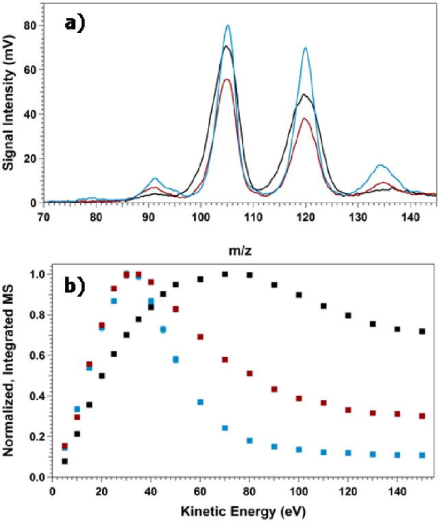
Figure 5.9: Mesitylene mass spectral signal intensity as a function of ion kinetic energy at 1.0 Torr and 0.5 Torr of air buffer gas. ...184
Figure 5.10: The lifetime of a Gen 9.1 microionizer operated in field emission mode in air buffer gas. ...185
LIST OF ABBREVIATIONS AND SYMBOLS
APCI atmospheric pressure chemical ionization
APGDI atmospheric pressure glow discharge ionization
ARDE aspect ratio dependent etch
ASU Arizona State University
CFE cold field emission
CHANL Chapel Hill Analytical and Nanofabrication Laboratory
CI chemical ionization
CID collision induced dissociation
CIT cylindrical ion trap
cm centimeter
CWA chemical warfare agent
CWS chemical warfare simulant
Da/s Dalton/second
DAPI discontinuous atmospheric pressure inlet
DART direct analysis in real time
DESI desorption electrospray ionization
DIMP diisopropylmethane phosphonate
DMA dimethyl aniline
DMMP dimethyl phosphonate
DRIE deep reactive ion etching
EI electron (impact) ionization
ESI electrospray ionization
ETE edge-to-edge emitter
eV electron-Volt
FI field ionization
FE field emission
FEA field emission array
FED field effect device
FET field effect transistor
GC gas chromatography
GD glow discharge
GDe negative mode GD
GDi positive mode GD
HPMS high pressure mass spectrometry
IE ionization energy
ITMS ion trap mass spectrometry
L liter
LD laser desorption
LOD limit of detection
lpi lines per inch
MALDI matrix assisted laser desorption ionization
m meter
mL milliliter
μm micrometer, micron
mm millimeter
mW milliwatt
MS mass spectrometry
MSn tandem mass spectrometry
m/z mass to charge ratio
ni nitride
nm nanometer
ORNL Oak Ridge National Laboratory
ox silicon dioxide
PCB printed circuit board
ppm part per million
QIT quadrupole ion trap
RIE reactive ion etching
RIT rectilinear ion trap
RF radio frequency
RVMD Rogue Valley Micro Devices, Inc
sccm standard cubic centimeter per minute
scfh standard cubic foot per hour
SEM scanning electron micrograph
SIM soft ionization membrane
SLIT stretched length ion trap
SOI silicon-on-insulator
SC single crystal
SNR signal-to-noise ratio
SWaP size, weight, and power
TIC toxic industrial compound
TOF time of flight
UA University of Arizona
UHP ultrahigh purity
UNC University of North Carolina
V Volt
Vp pulse voltage
Vb bias/float voltage
Vpp peak-to-peak voltage
V0-p zero-to-peak voltage
VME vacuum microelectronics
CHAPTER 1: INTRODUCTION – HIGH PRESSURE MASS SPECTROMETRY AND THE MICROIONIZER
1.1 Motivation for Handheld Mass Spectrometry
Among analytical instrumentation, mass spectrometry (MS) offers a unique combination
of selectivity, sensitivity, and speed and is often considered the gold standard for chemical
analysis.1 On-site, rapid chemical identification is important in many fields from
environmental protection to national security with analytes of interest including: toxic
industrial compounds (TIC); volatile organic compounds (VOC); explosives; and chemical
warfare agents (CWA).2 Mass spectrometry is the ideal technique for in-field analysis,
especially when informed (and potentially costly) decisions need to be made in a timely
manner for health and safety reasons. A recent example of this occurred in 2014 when
Freedom Industries spilled 10,000 gal of methylcyclohexane-methanol into the Elk River in
West Virginia.3 The Kanawha Valley water treatment plant attempted to process the
unknown, excess organics that suddenly appeared at the upstream side of the plant.
However, the carbon filtration system was quickly overwhelmed and a ‘Do Not Use’ order
was issued until these could be regenerated, leaving 300,000 residents without tap water for
weeks.4 Had the operators at the treatment plant access to a rapid, detailed chemical analysis,
quicker, informed decisions could have been made potentially avoiding the extended
downtime. Mass spectrometry would have been ideal for this situation; however, it is
Miniature mass spectrometers have been investigated for decades; the first suitcase-sized,
field portable mass spectrometer was disclosed in 19955 and currently, there are several
commercial systems available.6 Moreover, there is a demonstrated need for in-field mass
analysis.7 Despite availability and demand, mass spectrometry has yet to become ubiquitous
in the field because of size, cost, lack of robustness, and operator skill required. Many of the
field portable systems on the market share an important trait with their lab-sized counterparts
– cost both in capital (> $100k) and trained personnel to operate the instrument and interpret
data.
The Ramsey group at the University of North Carolina at Chapel Hill has focused on
bridging the divide – attempting to move mass spectrometry out of the laboratory and into
the field in a cost-friendly manner. The primary method for accomplishing this is to operate
the mass spectrometer at pressures negating the need for the most expensive, highest
power-consuming component, the turbomolecular pump. This pump elimination requires operation
at pressures greater than 100 mTorr. In comparison, traditional mass spectrometry requires
≤ 1 mTorr vacuum conditions and uses a two-stage pumping system, typically roughing +
turbo pumps. Operating the mass spectrometer at pressures ≥ 100 mTorr is referred to as
high pressure mass spectrometry (HPMS), which can be accomplished using simple
miniature-roughing pump with reasonable flow rates and continuous, atmospheric sampling.
Operating under HPMS conditions and atmospheric sampling requires that the three
major subsystems of the mass spectrometer (mass analyzer, ion detector, and ion source) be
compatible with a vacuum environment composed of ambient air. Because portability is a
objective was the development of a silicon-based solid state, field effect ionization source or
microionizer. Incorporating the microionizer within the HPMS system requires an
understanding of internal and external ion trapping under HPMS conditions, which was
performed with currently available MS ionization sources. HPMS with the microionizer
additionally required developing silicon microfabrication procedures; general instrument
design and construction; ion trap mass spectrometry (ITMS); and finally generating ions and
characterizing performance.
This chapter introduces the background necessary to understand the need for a low
power, field effect microionizer as well as the principle of operation behind the device.
Section 1.2 begins with a survey of current, miniaturized mass spectrometers. Section 1.3
highlights important theoretical details for HPMS as well as the current state of system
components used in HPMS research. Section 1.4 covers traditional ion sources that have
been coupled with mass spectrometry, including field effect devices; providing context for
the microionizer. Section 1.5 introduces field effect theory and highlights the progression of
field emission and field ionization devices. The microionizer is formally introduced in
Section 1.6. Finally, Section 1.7 provides an outline of the objectives for this dissertation.
1.2 Current Technology in Miniaturized Mass Spectrometers
Miniaturization of a mass spectrometer balances the needs of the intended application
(instrument performance) with the requirements for portability (size, weight, and power,
SWaP).6 This performance-portability trade-off covers a broad spectrum. On one end, when
resolving power is paramount then portability is sacrificed as seen with the refrigerator-sized,
miniature Fourier transform ion cyclotron resonance mass spectrometer (FT-ICR).8 On the
necessary to accomplish the task, such as the palm portable mass spectrometer which
samples at 0.02 Hz.9 The focus of HPMS is to raise instrument performance on the
portability end of the spectrum where SWaP is a premium. HPMS does this not only by
miniaturizing the hardware but also by adapting mass analysis in the high pressure regime (1
Torr vs. 1 mTorr).6, 10 To better understand the HPMS approach, a brief survey of
miniaturized mass analyzers is useful.
1.2.1 Miniaturized Mass Analyzers
Nearly every form of mass analyzer has been miniaturized8 and includes time of flight
(ToF);11 electric and magnetic sectors;12 linear quadrupole;13-14 and three-dimensional ion
traps.15-17 ToF and sector-based analyzers use static (or field-free) regions and require high
vacuum (less than 10-6 Torr) to maintain mass to charge ratio (m/z) separation. Linear
quadrupoles use both static DC and dynamic RF voltages to generate electric fields where a
single m/z is contained in two-dimensions and travels along the third to the detector. Since
ions are actively guided, linear quadrupoles can operate at higher pressures than TOF and
sectors; up to 0.01 Torr for highly miniaturized analyzers.18 Three-dimensional ion traps use
RF voltages to maintain a stable trapping volume at the center of the trap. Ion traps naturally
operate at high pressure (10-3 Torr) because the ion trajectory is completely defined by the
electric field, thus performance is less susceptible to ion-neutral scattering than the
previously mentioned mass analyzers.19 This has lead them to be the mass analyzer of choice
for the majority of miniaturized MS with portability as the key design factor.
1.2.2 Portable Ion Trap Mass Spectrometers
pressure tolerance, ion traps have two more desirable properties: mass resolution is
independent of trap size20 and the ability to perform tandem mass spectrometry (MSn).21-22
As such, considerable efforts have been placed into miniaturizing quadrupole ion traps
(QIT).23 One issue with the QIT is that it uses hyperbolic electrodes that become difficult to
fabricate at smaller scales (radius < 1 cm),24 which translates into higher costs for the mass
analyzer. An example is the toroidal ion trap, which has a large charge capacity (and hence
improved sensitivity) relative to a standard QIT, but is more difficult to fabricate.25
Geometric variants have been developed to overcome this issue including the rectilinear ion
trap (RIT)26 and the cylindrical ion trap (CIT).27 Each variant has been incorporated into a
miniature mass spectrometer such as: Guardion GC-MS (Smith Detection, Inc) based upon
the toroidal ion trap;28 the Mini-series of instruments from Purdue based upon the RIT;29-30
and the MMS-1000 (1st Detect, Inc) based upon the CIT.31-32 The Guardion GC-MS is a
ruggedized, briefcase-sized system which weighs > 30 lb and has less than 8 h battery life,
while the MMS-1000 is a small, lightweight benchtop system designed to be used with wall
power, thus it is best for stationary settings such as airport security checkpoints. The
Mini-series has variants covering the spectrum from hand-portable26 to benchtop.30
The Mini-instruments offer an interesting view into the miniaturization of the remaining subsystems of the mass spectrometer: the vacuum system, ion detector, and ion source. The vacuum system required is defined by the choice of mass analyzer and detector. The
resolution of the RIT is best at lower pressures (< 10 mTorr),33 which requires the use of a turbo pump. Miniature turbo pumps have been developed specifically for portable MS use,
but they are specialized, expensive, and fragile.34-35 Despite miniaturization, these pumps
the inclusion of a turbo pump increases SWaP, the low pressure enables the use of electron
multiplier tubes (EMT) or microchannel plates (MCP) for ion detection. Because these
devices have high sensitivity and bandwidth,37 there has yet to be a significant emphasis on
incorporating alternative (pressure tolerant) ion detectors.26, 30
Ion sources are a different matter because each source has strengths and weaknesses for
particular applications. Most miniature mass spectrometers are geared towards detecting
gaseous analytes, thus electron impact ionization (EI) is a staple and can be achieved via
thermionic emitters26 or plasma generators.29 Lower volatility analytes require ambient
ionization techniques and the Mini-instruments have been adapted for several methods
including low temperature plasma (LTP)35 and desorption electrospray ionization (DESI).38
However, each of these techniques requires sampling at atmospheric pressure, which strains
the vacuum system. The discontinuous atmospheric pressure interface (DAPI) was
introduced to counteract the increased power consumption caused by a constant gas load on a
turbo pump.39 In DAPI, an inlet is opened and a high gas load is imposed for sampling. The
inlet is then closed and a pump-down time is added to achieve < 10 mTorr operating range
for the RIT and EMT. Low pressure during mass analysis improves resolution and the
discontinuous gas flow improves battery life. However, DAPI limits data acquisition to
about 1 Hz as well as the maximum RF trapping voltage amplitude during ionization. This is
an example of a trade-off made to bridge the gap between person-portable and
hand-portability when a turbo pump is required for operation.6
The palm-portable mass spectrometer (PPMS) is an extreme example of DAPI. Similar
10-6 Torr) is achieved with a standard benchtop pumping system, then the PPMS is taken into
the field for use. The maximum sample rate is only 0.2 Hz. However, this rate exhausts the
getter’s limited capacity in under an hour. In order to achieve day-long operation, the
sampling rate is further reduced to just 0.02 Hz (≈ 1 sample/minute). The acquisition rate
and small sampling volume negatively impacts sensitivity and limits the applications
available to the PPMS. However, the PPMS represents a functional departure from
dependence on high-cost, fragile turbo pumping systems.30, 35
HPMS departs even further from the miniaturization efforts of the past and has been
successfully realized in a commercial mass spectrometer. The M908, introduced in 2014 by
908 Devices, Inc. fulfills the promise of a truly handheld mass spectrometer. This system is
based upon the theory of HPMS and is licensed technology from the Ramsey group.40 The
pumping system relies upon a custom, miniature roughing pump that maintains HPMS
conditions for a CIT-based trap design and pressure tolerant ion generation and detection.
The end result is a rugged, low-cost unit coming in at just 22.5 x 18.5 x 7.6 cm3 and 2.0 kg
(including battery)41 which is already being used in the field for threat detection such as
explosives and CWAs.42 The realization of handheld mass spectrometry has guided research
efforts to improve the three major subsystems (mass analyzer, ion detector, and ion source) in
order to continue lowering the cost and expand the utility and ubiquity of HPMS.
1.3 High Pressure Mass Analysis
To successfully develop an ionization source, an understanding of how ion traps work at higher pressures is necessary. The historical and theoretical groundwork for ion trap-based
HPMS has been thoroughly described elsewhere.43-45 Key topics regarding quadrupole ion
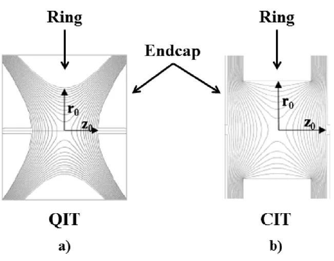
insulated electrodes – two grounded endcaps and a center ring electrode. For a QIT, the
electrodes follow a hyperbolic geometry, while a CIT is a cylindrical approximation. A cross
sectional view of the QIT vs. CIT can be seen in Figure 1.1. The critical dimensions of the
trap are defined as the radius of the ring electrode, r0, and the endcap-to-trap center spacing,
z0. A radio frequency (RF) potential applied to the center ring generates a quadrupolar
electric field and ions can oscillate in stable trajectories inside the field according to axial (az
and qz) and radial (ar and qr) stability parameters. These parameters are proportional to the
DC offset of the RF waveform (an) as well as the RF voltage amplitude (qn).46 Regions of
stable ion trajectory can be viewed using a stability diagram, shown by plotting the axial
stability parameters, az vs. qz.47 The stability diagram for a QIT is plotted in Figure 1.2,
which highlights the trapping conditions where ions exhibit both stable radial and axial
trajectories. HPMS utilizes mass selective instability mode developed by Stafford et al.48
which sets az = 0 and accumulates ions of various m/e (m/z) values inside the trap at low RF
amplitude according to:
qz = 8eV m(r02+2z
02)Ω2
(1.1)
Where the variables are the zero-to-peak RF voltage amplitude, V; RF angular frequency, Ω;
ion trap critical dimensions, r0 and z0; and inverse mass-to-charge, e/m. The RF amplitude is
linearly ramped and ions eject in order of their m/e when qz = 0.908. Goeringer et al.,49
theoretically determined the proportional relationship between mass resolution, Δm/m;
pressure, P, and RF angular frequency to be:
∆m m ∝
P Ω
suggesting that mass resolution could be maintained as buffer gas pressure increases (> 1 mTorr), provided RF frequency was increased. Whitten, et al. extended the theoretical work to higher pressures and showed resolution could be maintained at pressures upwards of 1 Torr by reducing the ion trap dimensions and increasing drive RF frequency.50 This is the core concept underpinning HPMS.
These theoretical investigations were followed by experimental confirmation. Cylindrical ion traps, with sub-millimeter critical dimensions (mCIT, r0 ≤ 0.5 mm) were
chosen because the QIT geometry is difficult to fabricate in miniature. Mass spectrometry was performed at low pressure helium (≈ 1 mTorr) using a mCIT with r0 = 0.5 mm, a 20-fold
decrease compared to a standard QIT (r0 = 10.0 mm), and the drive RF frequency was
5.8 MHz (f = 1.0 MHz for a standard QIT).15, 19, 51 These studies confirmed the theoretical relationships predicted by Whitten et al.; showing improved resolution and sensitivity by increasing RF frequency.15, 51 Subsequently, double resonant ejection was shown to reduce ejection voltage at both the 1/3 and 2/3 drive RF frequency resonances.52 More recently, HPMS has been demonstrated at 1 Torr helium, 53 nitrogen, and air;54 confirming the mass analyzer is capable of high pressure operation.
1.3.1 System Components for HPMS – Mass Analyzer
The initial high pressure studies used a mCIT with r0 = 0.5 mm and RF drive frequencies
ranging from 6 to 9 MHz.43, 45 They showed that with a constant RF frequency, peak widths
will increase (as predicted by Equation 1.2) as pressure increases. This loss in mass
resolution however can be regained by increasing the RF frequency.45 In order to maintain
stable ion trajectories, Equation 1.1 shows that increased RF frequency must be balanced
amplitude would be increased with the trap size maintained for charge capacity
considerations. However, there is a limit to the RF amplitude that can be applied at 1 Torr
due to electrical breakdown concerns.55 Experimentally, using smaller traps reduced the
applied RF amplitude needed with sub-dalton peak widths attained at 1 Torr in air buffer gas
at a drive frequency near 60 MHz with an mCIT of r0 = 100 µm.45
A trade-off here is that the reduction in trap size negatively impacts the potential well of
the ion trap leading to less sensitivity. For a QIT, the potential well depth, Dz, can be
approximated for qz less than 0.4:56
𝐷𝑧 ≈𝑞𝑧𝑉 8
(1.3)
where V is the same RF amplitude used in Equation 1.1. The potential well depth of a QIT
is a measure of its charge capacity, the maximum number of ions that can be trapped. For
reference, a typical, commercial ITMS has r0 = 1.00 cm and z0 = 0.783 cm and operates with
an RF frequency of 1.05 MHz with amplitude, 757 V0-p. While, a mCIT has r0 = 0.0500 cm
and z0 = 0.0645 cm and operates with an RF frequency of 6 MHz with amplitude near
150 V0-p. These values yield (roughly) a 4-fold decrease in well depth (10.5 vs. 42.5 V) for
the mCIT relative to a standard QIT. Assuming ion ejection and detection are equivalent, the
sensitivity of the mCIT is reduced compared to a standard QIT.
subsequently shown to improve charge capacity over a single-element mCIT under HPMS conditions.44, 59 Materials and fabrication techniques have also been investigated for improved trap operation.45
1.3.2 System Components for HPMS – Ion Detector
The operational pressure for HPMS, 1 Torr air buffer gas, is a demanding environment in
which to detect ions. To date, HPMS has relied upon two types of charge detectors: electron
multiplier tubes and faraday plates. While other charge detectors exist, such as image current
detectors, these have not been pursued (to date) due to long integration times.60 The EMT is
a staple detector for mass spectrometry because it has high gain, low noise, and high
bandwidth.61 Modern EMTs are continuous dynodes, where a large negative bias (typically
-1600 V) causes ions to impact the surface of the EMT which generates secondary electrons.62
These electrons are driven by the electric field into the tube, constantly colliding with the
surface and generating further secondary electrons ultimately yielding gains on the order of
106 electrons/ion.37, 63 Ion feedback, the generation of ions inside the EMT via EI, limits the
upper bounds of the pressure range to 10 mTorr.64 Despite the incompatible pressure range,
the EMT has been used extensively for HPMS development. This detector utilization was
accomplished by using a differentially pumped system with the EMT housed in a separate
detector vacuum chamber away from the mass analyzer (ion source and mCIT). Thus the
EMT can be held at pressures < 100 mTorr while the ion source and mCIT can operate at 1
Torr. This approach allows high pressure ion trap operation and decouples ion detector
development from that of the ion source and mass analyzer.43 Despite operating above the
pressures approaching 100 mTorr65 were performed by decreasing the applied voltage (thus
gain) applied to the EMT.45, 53
In addition to the EMT, pressure tolerant detectors have been shown to work at 1 Torr in
helium and air.43-44 These detectors collect charge using a faraday plate, then amplify and
convert the charge to a voltage, capable of direct measurement via a standard data acquisition
system (DAQ). Unfortunately, these detectors are more sensitive to electrical and
mechanical sources of noise (such as RF and vibrations) and have lower gains than EMTs.61
To combat these problems, HPMS specific amplifiers have been developed which reduce
noise, enabling higher gain operation.44, 66 There is also considerable interest in a solid state
equivalent to an EMT, which should combine the pressure tolerance of a faraday plate with the high gain and bandwidth of an EMT.67-68
1.3.3 System Components for HPMS – Ion Source
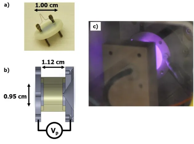
the work function, temperatures must exceed 1000 oC.70 Thus, thermionic emitters operate best at low pressure (due to collisional cooling effects), with gas compositions that avoid oxidative reactions. For HPMS studies, thermionic emitters were pushed to high pressure (1000 mTorr) in both helium and nitrogen for proof-of-concept studies but they suffered reduced lifetimes – likely a result of surface sputtering caused by ion back streaming.71 Air-based operation required the shift to glow discharge (Figure 1.3b). The source used for HPMS was designed for 1 Torr operation in air, with a 1 cm electrode separation and 1 cm electrode radius. However, a practical operational window of 250 to 2000 mTorr was achieved by tuning the voltage.54 An image of the characteristic purple glow of air-based operation can be seen in Figure 1.3c.
1.4 Advanced Ion Sources
To date, HPMS has focused on detecting airborne analytes (e.g. CWAs and VOCs) via
atmospheric sampling, thus EI via glow discharge-generated electrons has been the
workhorse ion source. Glow discharge is a serviceable ionization source for HPMS, but
there are inconvenient properties from a miniature, HPMS perspective. GD requires > 500 V
and a relatively large empty volume (≈ 0.8 cm3
) to generate the conditions necessary for
discharge.72 While the direct power consumption is on the order of 10 mW, the large volume
acts as a reservoir increasing the load on the vacuum pump and hence overall power
consumption of the instrument.
Alternatives to GD ionization are limited, but field effect devices (FED) hold promise as
ionization sources that are not only low power but also small in size thus reducing pumping
volume. The field effect refers to the behavior of electrons under intense electric fields and
of electrons from a surface into vacuum; while field ionization covers electron tunneling from a gas phase neutral into a surface.73 The quantum mechanical nature of the field effect requires no energy outside of that required to generate the electric field and a small
displacement current which makes it very attractive for portable and low-power
applications.74-75 The electric field strength necessary for field emission is near 10 MV/cm,76 while the threshold for field ionization is dependent upon the ionization potential of the neutral and ranges from 50 MV/cm for volatile organic molecules77 to 100 MV/cm for helium.78 Electric field strengths of this order are achieved via localized geometric field enhancement. A voltage is applied to a surface with a sharp tip creating an electric field between it and a counter-electrode. The presence of the high radius of curvature (< 1 nm) locally enhances the electric field and creates a field emission/ionization site dependent upon the amplitude and polarity of the applied potential. Early devices relied upon
electrochemically sharpened wires or edges that required greater than 5 kV to achieve field emission or ionization.79-80
The use of FEDs does not come without a price. Due to the small surface area, the emission current density at the tip can become very large, thus Joule heating limits the overall emission intensity.81-82 To overcome this, arrays of emission sites can be fabricated but require each tip to be nearly identical in order to ensure even field emission across the array. The precision required to produce identical emission tips across the array often incorporate time consuming or highly specialized steps into a complicated fabrication
The microionizer is a solid state, FED designed specifically with ease of fabrication in mind and geared toward HPMS operation. Proposed to fill this role by Dr. Stanley Pau, a collaborator at the University of Arizona, it offers two methods of ionization: direct field ionization and field emission-based EI. As designed, the microionizer does not rely upon
the formation of an array of identical sharp tips. Instead the inherent surface roughness from
the microfabrication process generates a massively redundant array of emission sites. Thus,
fabrication is based upon standard techniques, such as photolithography and deep reactive
ion etching.84 This should allow the microionizer to be produced at a fraction of the time and
cost of other microfabricated field effect devices. In order to better understand the
microionizer, it is useful to discuss current ionization techniques as well as field effect
devices used for mass spectrometry.
1.4.1 Internal vs. External Ionization
A host of ionization techniques have been developed in order to introduce analytes for mass spectral analysis.85 To date, HPMS has been focused on threat detection, for example
CWAs and VOCs, which are typically volatile. Thus, neutral gas is sampled from the
atmosphere into the mass analyzer where it is subsequently ionized. Depending on the
technique, ion generation occurs either internal or external to the trap. For an ion trap-based
mass spectrometer, there is an important distinction between whether an ion is generated internal or external of the trapping volume due to the pseudopotential well depth.86 In
addition to defining the charge capacity of the ion trap, it places an upper bound on the
kinetic energy an externally generated ion can have and still be successfully injected and
captured by the trap. Internally generated ions typically have thermal kinetic energies that
to 10 V), these ions are easily trapped. However, externally generated ions must be
transferred from the source into the trapping volume. Due to the dynamic nature of the three-dimensional trap, this means that the ion must not only be of low enough energy for capture, but it must also arrive at the proper phase of the RF cycle. For a traditional QITMS, estimates for the successful capture of externally generated ions are roughly 5%.
This capture percentage can be increased by several methods and include: 1)
Synchronization of the ion injection with the phase of the RF thereby minimizing the chances ions are scattered by the electric field as they pass into the ion trap.87-88 2) Modulation of the drive RF amplitude to better trap ions across a large mass range.89-90 3) Use of enhanced ion optics, such as ion funnels to increase the flux through the ion trap.91-92 4) Raise the buffer gas pressure as more buffer gas molecules act as a frictional force to cool ions into the potential well of the ion trap48, 9394 Of these techniques, the final one is most pertinent for HPMS since elevated buffer gas pressure is ever-present.
1.4.2 Ionization Methods for High Volatility Analytes
In-vacuum, ions are commonly generated using techniques such as electron impact ionization (EI), photoionization, chemical ionization (CI), plasma, and field ionization. Electron impact ionization is widely used throughout mass spectrometry; for example, NIST mass spectral standards are recorded with EI.95 However, EI requires neutrals to be easily introduced to vacuum (i.e. high vapor pressure), making it most useful for gas
chromatography-mass spectrometry (GC-MS); thermal desorption; headspace sampling; and continuous flow monitoring. It was used as a staple ionization source for the development of ITMS because it is capable of producing ions with thermal energy (25 meV assuming room
electron loss; an electron beam (typically 70 to 200 eV) is generated by a thermionic emitter, plasma, or cold cathode (field emitted) and guided through the ion trap. Electrons that interact with neutral analytes can impart enough energy to overcome the ionization potential and eject an electron from the neutral. The result is a positively charged molecular ion and two low energy electrons. Since the interaction is random, the molecular ion typically rearranges to access lower energy conformations resulting in a high degree of fragmentation; earning EI the status of a hard ionization source. EI based upon field emission is a
considered a viable route towards miniaturization.96
Chemical ionization (CI) was developed as an extension to EI. A gas, usually methane, is introduced to the vacuum in excess relative to the analyte. Subsequent EI of the methane produces ions (mainly CH5+ and C2H5+) that react with neutrals by proton or hydride
reactions yielding ionized products.97 CI increases the range of analytes accessible to mass spectral analysis, but still requires a highly volatile analyte. It also requires a consumable (methane), which makes it less amenable to miniaturization. However, atmospheric pressure chemical ionization (APCI) holds promise as an ionization technique for portable
instrumentation since it relies upon ion-driven chemical reactions with nitrogen-based radicals generated from ambient air.98-99
Photoionization utilizes photons to ionize neutral molecules - a photon of energy greater than the ionization potential of the neutral (typically ultraviolet) must be absorbed for
In addition to its utility as an electron source for EI, glow discharge plasmas can be used as external ion sources as well by directly sampling the plasma.101 Two electrodes are immersed in a gas (noble, nitrogen, or air) and a voltage is applied between them initiating a Townsend discharge.99, 102 The discharge will sustain if the field strength, separation
between electrodes, and pressure meet the Paschen breakdown conditions.103 Ions can be generated in several ways using GD. Gaseous analyte can be ionized and sampled directly from the plasma or a material can be placed on the cathode and ablated via ion
bombardment.101 GD has gained popularity in mass spectrometry due to its simplicity – a feature that translates well to portable instrumentation.29, 104-105
Field ionization relies upon the behavior of electrons at high electric field strengths, where electrons can tunnel from a neutral analyte into vacuum in the presence of a sufficient electric field (> 50 MV/cm).78 The electric field strengths are achieved by applying a large voltage (> 5 kV) to a chemically sharpened wire or razor blade (with radius of curvature measured in nanometers).79 As neutral molecules pass near the tip, the most loosely bound electrons can tunnel into the ionization tip, yielding singly charged, positive ions.77, 106 This technique has been successfully coupled with mass spectrometry,107-108 and it is considered soft because of the dominant molecular ion peak and lack of fragmentation.109
1.4.3 Field Effect Devices for Mass Spectrometry
an ITMS for the European Space Agency’s Rosetta mission that was launched in 2004 and began providing results in 2014.112-113 Applications of FEDs aimed towards field portability include diamond-coated silicon whiskers coupled with a mCIT (Figure 1.4b)114 and a carbon nanotube-based EI source for a handheld magnetic sector MS (Figure 1.4c).12, 115 Field ionization sources gained traction with mass spectrometry as the first known soft ionization source.116 This helped obtain spectra of complex samples using lower resolution
instrumentation.109
Modern microfabrication procedures (photolithography, reactive ion etching, and thin film deposition) have led to the rise of vacuum microelectronics (VME). Previous FEDs were typically sharpened wires or edges and required ≥ 5 kV to generate field strengths necessary for the field effect.76 At these high potentials, the ions formed acquire significant kinetic energy (on the order of keVs) resulting in significant transmission losses into the mass analyzer. With the advent of VMEs, lower potentials (near 500 V) can generate the same field strengths, improving ion transmission and opening up the possibility of coupling with ITMS.107 Microfabricated field ion sources for mass spectrometry have been studied, though not quite as prolifically as field emission-based sources.110 The micro-volcano (Figure 1.4d)107 was the first VME field ionizer to be coupled with mass spectrometry.110
The combination of small size, low-power, and the ability to perform both EI (based upon field emitted electrons) as well as field ionization have made field effect devices a prime target for combining with mass spectrometry. Despite these advantages, field effect devices have not displaced traditional sources such as thermionic-based EI because of economics. FEDs are simply too expensive relative to their traditional counterparts, except where circumstances prioritize performance over price, such as the Rosetta comet exploratory mission.112-113
1.5 Field Effect Applications and Theory
Mass spectrometry is only one of many potential applications for field effect devices. Charge generation is important in many research areas and field emission has been applied to field effect displays;83 x-ray tubes;117 field effect transistors;118 and vacuum RF amplifiers such as the traveling wave tube.119 While thermionic emitters suffice for these technologies, the general push towards smaller, more efficient devices makes FEDs highly desirable. For example, the power required for the average cellular phone tower could drop by orders of magnitude if the microwave amplifiers could utilize cold cathodes in place of thermionic electron sources.119 Field ionization also has several applications beyond mass spectrometry including high resolution ion microscopy;78, 120 ion sources;121-122 gas detectors;123-124
portable neutron generators;121 and ion thrusters for microsatellites.125 Given the array of applications that FEDs can help revolutionize, it is important to understand the theory behind them.
1.5.1 Field Emission
Field emission is often referred to as cold field emission (CFE) because it occurs at room
Nordheim used a triangular barrier approximation for electron emission to quantify field emission current density from a planar, metallic surface as a function of electric field strength and work function.127 The standard, temperature independent form is as follows:128
𝑗0 =
𝑎 𝑡𝐹2𝜑𝐹2𝑒
−𝑣𝐹 𝑏 𝜑3/2
𝐹 (1.10)
where, the subscript ‘0’ refers to the temperature and the variables are: φ, surface work function; F, the electric field; tF-2 and vF are elliptical functions referring to the
Schottky-Nordheim barrier;129 a and b are the Fowler-Nordheim constants which are defined as:128, 130
𝑎 ≡ 𝑒
3
8𝜋ℎ𝑝 ≈ 1.541 𝐴 𝑒𝑉
𝑉2
(1.11)
𝑏 ≡ 8𝜋𝑒ℎ𝑝 3√2𝑚𝑒
≈ 6.831 𝑥 107 𝑉 𝑒𝑉3/2𝑐𝑚
(1.12)
and e is the elementary charge; hp is Plank’s constant; and me is the mass of the electron.
In 1956, Murphy and Good generalized electron emission from a metallic surface to include temperature and found that Fowler-Nordheim was the zero-temperature limit of their expression.129 In 1976, Spindt approximated the elliptical functions, tF-2 and vF in order to
use field emission current measurements to extract the emitter surface area, α and field enhancement factor, β where:131
𝑗 = 𝐼 𝛼
(1.13)
𝐹 = 𝛽 𝑉 (1.14)
The theory presented to this point is also specific to metallic surfaces. Semiconductor-based field emission requires additional consideration and depends upon the doping.76 Deviations from standard Fowler-Nordheim field emission are observed for p-type and lightly-doped (< 1018 dopants/cm3 in silicon) n-type semiconductors. For p-type
semiconductors, electron emission into vacuum creates an inversion layer at the surface. While the surface work function is typically lower for a p-type semiconductor,134-135 it does not compensate for the alteration of the electric field due to penetration into the crystal and emission is reduced relative to an analogous structure in metal.136 For lightly doped (high resistivity) n-type semiconductors, the rate of carrier (electron) generation is limited and is often smaller than the rate at which electrons are emitted into vacuum, again resulting in reduced emission relative to a metal surface.136 For highly-doped n-type semiconductors (> 1018 dopants/cm3 in silicon), field emission typically follows standard Fowler-Nordheim theory.74 For this reason, highly-doped silicon was predominately used for microionizer fabrication.
A note regarding field emission in general: due to the highly-localized nature of emission sites, quantitative analysis has been described as ‘messy’ by experts in the field.73 More often than not, several variables in the Fowler-Nordheim (even the elementary version) are unknown such as the work function and radius of curvature of the emission site. As such, calculated field enhancement factors, work functions, and emission current densities
For many field emission sources, the microionizer included, Fowler-Nordheim analysis is used simply to verify field emission as the mechanism behind observed electron currents.
1.5.2 Field Ionization
Field ionization is a complement to field emission, where an electron from a neutral atom or molecule can tunnel into a surface.76 Since the Fermi level is nearly full in a conductor, the electron must tunnel into an energy level above this, and a simple one-dimensional model is used to describe the energy of the neutral orbital, ϵ, relative to the Fermi level:73
𝜖 = (𝐼1− 𝜑) + 𝑒𝐹𝑥 (1.15)
where the variables are: the first ionization potential of the neutral, I1 and the separation
distance between the nucleus of the neutral and ionization tip, x. A critical distance, xc, is
defined when ϵ = 0. The electron cannot tunnel directly when x < xc, since this would place
it below the Fermi level of the conductor. Thus, field ionization occurs outside of this critical distance while field desorption and/or tunneling through an adsorbed layer is believed to occur within the critical distance:116
𝑥𝑐 ≅ (𝐼1− 𝜑) 𝑒𝐹
(1.15)
Ionization can be estimated to occur with 1 nm of the critical distance and the efficiency is dependent upon the time a neutral spends within this distance of the surface.124 Field ionization demonstrates a threshold behavior, where neutrals with different ionization
1.5.3 Pressure Tolerance and Lifetime
For field emission a large negative potential is typically required to generate the requisite electric field. Many field emitters are designed to be operated at high vacuum (< 10-6 Torr), and can maintain >50% emission of their original emission intensity after more than 10,000 h of operation.74 This mark is especially important for applications where the FED cannot be easily serviced and/or replaced such as computer displays.83 High vacuum reduces sputtering damage at the emission site due to ion back streaming. Back streaming involves ions formed via EI events near the FED that are accelerated opposite of the electrons and crash into the surface. This backstream of ions will gain energy equal to the potential applied to the tip, thus they can easily hit the threshold for ion-induced surface damage and sputtering138 degrading the emission tip.81 Tip degradation is of concern, because it can lead to emission-induced failure. The emission current density has an exponential dependence upon work function and emitter tip geometry; thus small changes such as adsorbed gases or emitter tip deformation can cause large deviations in the field emission current, resulting in emitter damage.139-140 If the emission is spread across an array (as is common) the failure of a single tip results in outgassing which will briefly increase the rate of ion backstream sputtering as well as neutral adsorption leading to premature failure in the surrounding tips.75, 81 This problem can be avoided by adding a current limiting (ballast) resistor in series with each tip, which adds complexity and cost to the fabrication process.141 At higher pressure, 10-3 to 10-5 Torr, surface flashover becomes a concern. As the name implies, it is a surface effect, where charge buildup on the insulator layer of a gated field emitter can aid in the formation of a plasma that can result in an arc discharge between the anode and cathode of the field
Field ionizers can suffer from many of the same failure mechanisms as field emission sources, such as dielectric breakdown and surface flashover.80, 124, 144 Due to the increase in field strength for field ionization, dielectric breakdown is a more common occurrence than in field emission. Breakdown is accelerated by electron injection into the dielectric, which can degrade the insulator over time.145-147 Additionally, field desorption can gradually erode the tip leading to reduced signal intensity over time.144 Despite the greater difficulty of working at higher field strengths, field ionization has one advantage over field emission: the opposite polarity of the applied potential prevents ion back streaming damage since ions flow away from the ionization tip.124 Thus, pressure limitations are more likely to originate from standard Paschen-type breakdowns to any nearby ground planes. Similar to field emission sources, well designed field ionization sources have demonstrated lifetimes longer than 10,000 h.110
1.5.4 Fabrication
Both field emission and field ionization devices have functional limitations, with some materials better suited than others. For example, refractory metals have high melting points, making them ideal for high current density applications where localized Joule heating can induce premature tip erosion.139 As such a host of materials have been studied including: carbon nanotubes;148-149 porous silicon carbide;150 thin-film semiconductors;151-152 metal and diamond coated semiconductors;131, 153-154 CVD diamond;137 among many other examples.132
important properties: first, the spacing between the emission tip and counter-electrode can be precisely controlled on the micrometer scale, reducing the potentials necessary for field emission below 1 kV; second, arrays of parallel emission sites or field emission arrays (FEA) with nearly identical dimensions can be fabricated.75, 110 These FEA of single-point emitters produce more consistent field emission and field ionization compared to single points (as opposed to large edges).79 Despite the ‘ease’ with which microfabrication enables arrays to be generated, the exponential dependence of the current density upon tip geometry and work function means that the process must be tightly controlled. Each tip should be identical down to the nanometer scale, which is a difficult task that adds time and cost to fabricaiton.132 Techniques have been developed to ‘burn in’ devices, such as quickly ramping the field strength up and down in order to burn off the sharpest tips, but the array fabrication must still be tightly controlled.155
1.6 Solid State Microionizer
1.6.1 Design and Operation
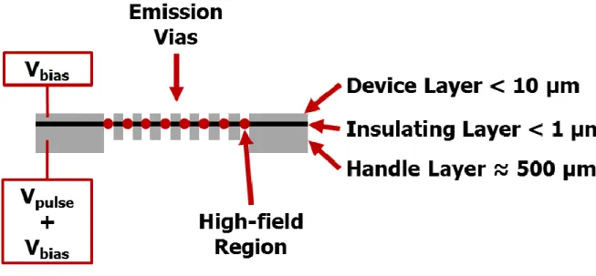
high field region) of about 100 µm. At this thickness, an electric field strength of 1 MV/cm necessary for field emission would require a potential of 10 kV. As the goal is to minimize the applied voltage, preferably below 100 V, the spacing between electrodes should be on the order of 1 µm or less to produce 1 MV/cm field strengths.
The microionizer relies upon silicon-on-insulator (SOI) substrates to achieve ≤ 1 µm spacing for the high field region. SOI is a layered structure, where an insulator, typically oxide, separates two, parallel silicon layers (the device and handle).162 A cross sectional schematic of the microionizer is shown in Figure 1.5; the SOI layers as well as the high-field region are highlighted. SOI can be made-to-order and the thicknesses of all three layers are customizable as well as dopant type and concentration. A 150 mm (6”) SOI substrate can have device layers ranging from 2 to 150 µm; insulator layers from 0.1 to 10 µm; and handle layers from 400 to 650 µm.163 SOI has been primarily used for low-power microprocessors
because the electrical isolation of the device layer reduces parasitic capacitance during high
speed switching.164-165 However, the wide range of layer thicknesses has also positioned SOI
as an invaluable substrate in applications ranging from photonics to microelectromechanical systems (MEMS).166-168 For the microionizer, the insulator layer thicknesses available are ideal for sub-100 V operating voltages.
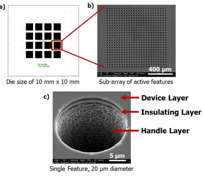
The first generation microionizer utilized SOI with highly-doped, n-type silicon, separated by a 0.5 µm oxide. The original layout is shown in Figure 1.6a and consists of a 1 cm2 die with a 4 x 4 array of active features; the device and handle layers are 2 and 400 µm thick, respectively. The vias shown in Figure 1.6b and c are cylindrical with a 20 µm
applied to the microionizer are shown in Figure 1.5. The pulse voltage initiates field
emission or field ionization while the bias voltage controls the electron/ion energy relative to the mCIT. For the 0.5 µm thick insulating layer, only 50 V is needed to achieve 1 MV/cm electric field strength. Geometric field enhancement due to surface roughness generated by the etch process (seen in Figure 1.6c) should boost the macroscopic field into the 10 to 100 MV/cm necessary for field emission and field ionization.150
1.6.2 Examples of Similar FEDs
There is precedent in the literature for similar FED devices, but none combine the ease of fabrication and dual-role nature of the microionizer. Planar devices using thin insulating layers have been fabricated for field ionization and field emission. A soft ionization
1.6.3 Advantages of the Microionizer
The key to success for the microionizer relative to other FEDs lies in its design. It is specifically meant for HPMS, which means pressure tolerance, power consumption, and fabrication costs were key design considerations. Other field emission devices rarely operate at pressures higher than 10-6 Torr due to ion back streaming.132 For the microionizer, back stream-induced sputtering should be minimized. The thinner insulating layer between handle and device layer of the SOI wafer requires smaller potentials to generate the macroscopic electric field strengths necessary for field emission. Thus, ions formed due to EI will only be able to gain limited kinetic energy (< 100 eV). Moreover, the difference in mean free paths of electrons and ions means that most of the back stream ions generated by EI will undergo collisions prior to impact with the emitter tip. This should retard their ability to sputter the emission tip. While thinner insulating layers lead to improved pressure tolerance, they also reduce power consumption. Reduction of the insulating layer thickness yields similar macroscopic field strengths at lower operating voltages. Since the displacement current is a function of electric field strength, lower voltages will yield lower power consumption. Ultimately, the circuitry required to generate the pulse can be simplified as the voltage amplitude decreases which will also reduce secondary power consumption.172
The microionizer achieves field effect by geometric enhancement due to the surface roughness of the device sidewalls. Many other FED’s use arrays of identically sharpened tips. By relying upon the surface roughness, the stringent fabrication requirements for nanometer-level precision are not necessary. This also means the process is less susceptible to variations in etches and depositions across the entire surface area of a single wafer.
fabrication steps (a list of the tools and techniques used for microionizer fabrication can be found in Appendix A). The end result is that microionizer fabrication can use more surface area of the wafer while simultaneously maintaining a better overall yield than other FEDs. Thus, the cost per device should be lower for the microionizer.
1.7 Objectives and Roadmap
The work presented in this dissertation focuses on developing a pressure and oxygen
tolerant ion generation source (microionizer) for use with high pressure mass spectrometry.
The original specific aims proposed in 2012, were: 1) demonstrate field emission and field
ionization-based high pressure mass spectrometry using a microionizer; 2) determine lifetime
and controlling parameters for the microionizer; and 3) integrate the microionizer into a
mCIT trap electrode stack.
The work began with investigating traditional ionization sources under HPMS conditions and finished with successful microionizer-based HPMS. Chapter 2 reports the results of internal and external ionization under HPMS conditions using traditional ionization sources. Chapter 3 covers proof of concept experiments with the initial microionizer design providing important design and operational condition insights for successful field emission and field ionization. Chapter 4 documents the development of the fabrication process flow for
1.8 Figures
Figure 1.2: Stability diagram for the z-dimension of a QIT. The axes are the stability parameters where az is proportional to the DC offset and qz to the RF amplitude. The β lines
are thresholds between stable, periodic motion in each direction. The red line at az = 0 is the
typical region over which a QITMS operates in mass selective instability mode. Ions order themselves inversely proportional to qz; as the RF amplitude is increased ions eject axially
Figure 1.4: Examples of field effect devices used for mass spectrometry. a) An array of Spindt cathodes used as an electron source for EI with a linear quadrupole.75 b) CVD
1.9 REFERENCES
1. de Hoffmann, E.; Stroobant, V., Mass Spectrometry Principles and Applications. 3rd ed.; John Wiley & Sons: West Sussex, England, 2009; p 489.
2. McClennen, W. H., et al., Field-portable hypenated instrumentation: the birth of the tricorder? Trends in Analytical Chemistry 1994, 13 (7), 286-293.
3. McGuire, M. J., et al., An unwanted licorice odor in a West Virginia water supply. J
Am Water Works Ass 2014, 106 (6), 72-82.
4. Manuel, J., Crisis and Emergency Risk Communication: Lessons from the Elk River Spill. Environ Health Persp 2014, 122 (8), A214-A219.
5. Bryden, W. A., et al., The Tiny-Tof Mass-Spectrometer for Chemical and Biological Sensing. J Hopkins Apl Tech D 1995, 16 (3), 296-310.
6. Lammert, S. A., Field Portable Mass Spectrometry. In Detection of chemical, biological, radiological and nuclear agents for the prevention of terrorism : mass
spectrometry and allied topics, Banoub, J., Ed. Springer: New York, 2014; p 291.
7. Hoffmann, W. D.; Jackson, G. P., Forensic Mass Spectrometry. In Annual Review of
Analytical Chemistry, Vol 8, Cooks, R. G.; Pemberton, J. E., Eds. Annual Reviews:
Palo Alto, 2015; Vol. 8, pp 419-440.
8. Badman, E. R.; Cooks, R. G., Special feature: Perspective - Miniature mass analyzers.
J. Mass Spectrom. 2000, 35 (6), 659-671.
9. Yang, M., et al., Development of a Palm Portable Mass Spectrometer. J. Am. Soc.
Mass Spectrom. 2008, 19 (10), 1442-1448.
10. Ouyang, Z., et al., Handheld Miniature Ion Trap Mass Spectrometers. Analytical
chemistry 2009, 81 (7), 2421-2425.
11. Bryden, W. A., et al., Tiny-TOF-MALDI mass spectrometry for particulate drug and explosives detection. Law Enforcement Technologies: Identification Technologies