Multi-Valued Logic Circuit Design and
Implementation
Ben Choi and Kankana Shukla
Computer Science, Louisiana Tech University, USA Email: [email protected]
Abstract
—
To further increase the speed of computation, this paper aims to design and implement digital circuits entirely within the domain of multi-valued logic. In a four-valued logic circuit, each wire carries two bits at a time, each logic gate operates two bits at once, and each memory cell records two bits at one time. To make the multi-valued computation possible, this paper describes a simple four-step process for designing multi-valued circuits to implement any multi-valued functions. The design of a four-valued adder is provided as an example. This paper also contributes new designs for multi-valued memory and flip-flops, which can be extended to be used for infinite-valued or Fuzzy logic circuits, for fully exploiting many-valued logic and fuzzy paradigm in hardware. The multi-valued circuit design methodology and the multi-valued memory provide the necessary and sufficient tools and components for designing multi-valued systems entirely within the domain of multi-valued logic. Index Terms—multi-valued logic, fuzzy control, circuit design, fuzzy memory, fuzzy system
I. INTRODUCTION
The performances of current computers are reaching their limits. Almost all present day computers are built based on two-valued logic. In two-valued logic, each wire can have two states. The performance of current computer depends mostly on how quickly the states can be changed, which determines the clock speed. During the past decades, the clock speed for CPU had doubled almost every year. In recent years, the clock speed doubled every 18 months. Now, it has become progressively difficult to increase the clock speed. The limit is approaching. Recently, CPU manufacturers are trying to circumvent the limitation of clock speed by packing more and more “cores” into a chip, which has resulted in dual-core or quad-core CPUs. However, this multi-core approach does not greatly improve the performance. This is due in part by the limit of the amount of data that can be transferred between the CPU and its connected components, which is determined by the number of pins on the CPU. Using two-value logic each pin on the CPU can have at most two states, and again the amount of data that can be transferred is determined by the clock speed. Thus, the multi-core approach does not circumvent the limitation.
Manuscript received April 15, 2014; revised July 18, 2014.
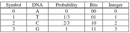
Thus, there is a need for an innovative approach in order to push the speed limit of computing. Now is the time to depart from the two-valued logic to venture into multi-valued logic and even into infinite-valued (Fuzzy) logic. Advancing from two-valued to four-valued logic provides an progressive approach [1]. Four symbols {0, 1, 2, 3} are needed to distinguish the four values, as shown in Table I. The four values might represent anything, for example, the four bases {A, T, C, G} found in DNA, or probability {0, 1/3, 2/3, 1}. These four values can be converted to binary numbers {00, 01, 10, 11}, or they can simply represent integers {0, 1, 2, 3}. It is also possible to start from the ground up by designing components needed for constructing four-valued logic circuits. Each four-valued logic gates will operate two bits of data at a time, and each memory cell will record two bits at once. Now, each wire or CPU pin can have four states, which could double the amount of data that can be transferred between the CPU and its connected components without increasing the number of pins on the CPU. With eight-valued logic, each logic gate operates three bits of data and CPU pin carries three bits of data. The extreme case will be the infinite-valued or Fuzzy logic. Now, a different limit is being pushed.
TABLE I. REPRESENTATIONS FOR A FOUR-VALUED VARIABLE
Symbol DNA Probability Bits Integer 0 A 0 00 0 1 T 1/3 01 1 2 C 2/3 10 2 3 G 1 11 3
To make the multi-valued computation possible, this paper provides the necessary and sufficient tools and components for designing multi-valued systems entirely within the domain of multi-valued logic. We describe a simple four-step process for designing multi-valued circuits to implement any multi-valued functions. The design of a four-valued adder is provided as an example. By following the simple four-step process, it becomes very convenient to design multi-valued circuits to implement any multi-valued functions. We also provide new designs for multi-valued memory and flip-flops, which can be extended to be used for infinite-valued or Fuzzy logic circuits, for fully exploiting many-valued logic and fuzzy paradigm in hardware.
limitations. Section III describes using Post Algebra as the mathematical foundation that facilitates the design process of multi-valued circuits. Section IV outlines our simple four-step process for designing multi-valued circuits to implement any multi-valued functions. Section V shows our design of multi-value memory and flip-flops. Section VI gives the conclusion and outlines the future research.
II. RELATED RESEARCH
To exploit the multi-valued computation in hardware, we need the fundamental building blocks for multi-valued logic circuits: multi-multi-valued logic gates, memory cells, and flip-flops. However, even these essential logic gates and memory cells are not yet fully developed. Currently, many-valued and fuzzy systems [2]-[8] are usually simulated or implemented by using a fuzzifier to convert the inputs, using a set of fuzzy rulesfor processing and inferring, and using a defuzzifier to convert the results to outputs. To go a step further, researchers are now researching on many-valued and fuzzy logic circuits that can fully implement fuzzy systems.
To make the transition from two-valued to many-valued logic circuits, researchers were attempting to adapt CMOS [9], [10] technologies to implement the many-valued and Fuzzy logic gates. The design of the AND gate and the OR gate using CMOS technology was reported [1], [11]-[13]. Other researchers used analog circuits to implement the many-valued and fuzzy logic gates [14]-[17]. However, these analog circuits were more difficult to be fabricated.
Many-valued and fuzzy memory cells or fuzzy flip-flops were proposed in [8], [18]-[26]. Concept of fuzzy flip-flop was first mentioned by Hirota [18]. They used analog gates [27]-[29] for the design their JK-type flip-flop as discussed in [14]. Hirota[18]defined fuzzy JK flip-flop based on the binary JK flip-flop but using fuzzy operators. Their design was based on fuzzy operators such as t-norm, s-norm, and fuzzy negation. Consider two fuzzy sets x and y in universe of discourse U, a S-norm operation [30] is defined as,
)}],
(
),
(
max[
)
(
u
xu
yu
y
x
u
U
T-norm operation is defined as
)}], ( ), ( min[ )
(u x u y u
y
x
u
U
Fuzzy negation is defined as follows:
), ( 1 )
(u x u
x
u
U
Based on the fuzzy operations, Hirota [18] defined set-type and reset-set-type fuzzy flip-flop. Reset-set-type fuzzy JK flip-flop has the following characteristic equation:
1 ()
1
( )
)1
(t J Qt K Qt
QR
Characteristic equation for set-type JKfuzzy flip-flop is as follows
()
1
1 ()
) 1
(t J Qt K Qt
QS
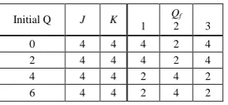
TABLE II. ONE UNSTABLE CONDITION FOR THE SET-TYPE OR RESET -TYPE JKFUZZY FLIP-FLOP
Initial Q J K
1
Qf
2 3 0 4 4 4 2 4 2 4 4 4 2 4 4 4 4 2 4 2 6 4 4 2 4 2
We found several unstable conditions for the set-type and the reset-type JK fuzzy flip-flop defined above. Some such examples are provided in Table II. While the initial stored value of Q is 0v and when given 4v for inputs J and K, the resulting Q will continuously toggling between 4v and 2v. Similar unstable conditions appears when initial stored value is 2v and given 4v for inputs J and K. Other unstable conditions was also observed, but not shown in the table, for values J=K=6, J=4 K=6, and J=6 K=4.
Therefore, neither the set-type nor the reset-type alone can be used as a fuzzy flip-flop. Hirota [18] combined the characteristics of both set-type and reset-type fuzzy JK flip flop and introduced a fundamental equation for fuzzy JK flip flop. The characteristic equation for min-max type fuzzy JK flip flop is as follows:
()
()
) 1
(t J K J Qt K Qt
Q
However, above equation also produced unstable conditions such as some shown in Table II. The researchers tried to eliminate the above unstable conditions by introducing a pair of complicated sample and hold circuits. The sample and hold circuits latch the output during each clock pulse, thus emulating the behavior of aflip-flop. However, these circuits were difficult to design and cumber some to modify. Such circuits cannot easily be combined with other fuzzy circuits.
Virant et al. [24] proposed a design of T-type fuzzy flip-flop. The researchers adapted a strategy similar to Hirota [18]in the design of the T fuzzy flip-flop. They introduced the following two equations for T fuzzy flip-flop[24]:
min 1 , (),min ,1 ()
max ) 1
(t T Qt T Qt
Q
max , (),max 1 ,1 ()
min) 1
(t T Qt T Qt
Q
However, the T fuzzy flip-flop has its own limitation. For example, it cannot be connected in such a way to produce a D-type fuzzy flip-flop.
memory cell can store any value ranging from zero to one, such as the four-valued case {0, 1/3, 2/3, 1}. Furthermore, it was built entirely based on fuzzy logic gates.
III. USING POST ALGEBRA AS FOUNDATION FOR
MULTI-VALUED CIRCUIT DESIGN
This section describes the mathematical foundation of multi-valued logic that facilitates the design process of multi-valued circuits. While Boolean algebra provides the mathematical foundation for designing two-valued digital circuits, Post algebra provides the mathematical foundation for designing multi-valued circuits. We choose the disjoint system of Post algebras of order n≥2 for the reason that the disjoint system facilitates simple design processes (described in Section 4). The postulates for a disjoint system of Post algebras is provided in the following table (based on [31]).
TABLE III. POSTULATES FOR DISJOINT SYSTEM OF POST ALGEBRAS OF ORDER N≥2
P1 A·B = B·A A+B = B+A (A·B)·C = A·(B·C) (A+B)+C = A+(B+C) A·A = A A+A = A
(A+B)·A = A (A·B)+A = A A·(B+C) = (A·B)+(A·C)
P2 en-1·A = A e0+A = A
ei·ei+1= ei for 0<i<n-2
P3 Ci(A)·Cj(A) = e0
for i ≠ j, 0 ≤ i, j ≤ n-1 C0(A)+C1 (A)+…+ Cn-2(A)+Cn-1(A) = en-1
P4 Ci(A·B) =
Ci(A)·[Ci(B)+Ci+1(B)+…
+Cn-1(B)] +
Ci(B)·[Ci(A)+Ci+1(A)+…
+Cn-1(A)]
for i = 0,1,…,n-1
Cn-1(A+B) =
Cn-1(A)+Cn-1(B)
P5 Ci(ej) = e0 for i ≠ j, 0 ≤ i, j ≤ n-1
Cn-1(e0) = e0
Cn-1(en-2) = e0
P6 e1·C1(A)+e2·C2(A)+…+en-1·Cn-1(A) = A
Table III defines a disjoin system of Post algebras of order n≥2. Where, the A, B, and C are n-valued variables. The ei for 0 ≤ i ≤ n-1 are n constants. The Ci(x) for 0 ≤ i
≤ n-1 are n disjoint unary operations. The •is the binary operation that represents AND, while the + is the binary operation that represents OR.
TABLE IV. BOOLEAN ALGEBRAS ARE POST ALGEBRAS OF ORDER 2 Input Output
NOT(A) = A = A C0(A) C1(A)
F = e0 0 1 0
T = e1 1 0 1
Boolean algebras are Post algebras of order 2 as highlighted in Table IV. There are two constants: e0
denoted by 0, and e1 denoted by 1. The Boolean NOT(A)
= C0(A), while C1(A) = A. The • is equivalent to the
Boolean AND operation, while the + is equivalent to the Boolean OR operation.
In the following, we choose, as an example, the disjoint system of Post algebras of order n = 4, and called the system a four-valued logic. As outlined in the following table, we use A as a 4-valued variable. The 4 constants are denoted by 0, 1, 2, 3, are the 4 disjoint unary operations C0(A), C1(A), C2(A), and C3(A) are
defined as shown in Table V.
TABLE V. POST ALGEBRAS OF ORDER 4(FOUR-VALUED LOGIC) Input Output
A C0(A) C1(A) C2(A) C3(A)
F=e0 0 3 0 0 0
e1 1 0 3 0 0
e2 2 0 0 3 0
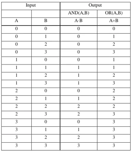
T=e3 3 0 0 0 3 The 4-valued AND, OR operations are defined as shown in Table VI, where the AND operation produce as output the minimum of (A, B), while the OR operation produce as output the Maximum of (A, B).
TABLE VI. FOUR-VALUED AND(MIN),OR(MAX) Input Output
AND(A,B) OR(A,B) A B A·B A+B
0 0 0 0 0 1 0 1 0 2 0 2 0 3 0 3 1 0 0 1 1 1 1 1 1 2 1 2 1 3 1 3 2 0 0 2 2 1 1 2 2 2 2 2 2 3 2 3 3 0 0 3 3 1 1 3 3 2 2 3 3 3 3 3
IV. SIMPLE FOUR-STEP PROCESS FOR DESIGNING
MULTI-VALUED CIRCUITS
Based on the disjoint system of Post algebras of order n≥2 defined in Section III, we outline a simple four-step process for designing multi-valued circuits to implement any multi-valued functions. The four steps are: (0) Creating a truth table to define the function; (1) Connecting each input x to n Ci(x) gates; (2) Creating an
four-TABLE VII. TRUTH TABLE DEFINING A FOUR-VALUED ADDER
Input Output 41x 40x
A B K S 0 0 0 0 0 1 0 1 0 2 0 2 0 3 0 3 1 0 0 1 1 1 0 2 1 2 0 3 1 3 1 0 2 0 0 2 2 1 0 3 2 2 1 0 2 3 1 1 3 0 0 3 3 1 1 0 3 2 1 1 3 3 1 2
As shown in Table VII, all possible input combinations are shown in column A and B. The results of the addition is encoded by two outputs K and S, where K stands for carry and S stands for sum, and the total value is 4K+S. The column K defines the function required to produce K as output, and the column S defines the function required to produce S as output.
Continuing the above example of designing an adder, the adder have two inputs, A and B. Now, we connect input A to 4 Ci(A) gates:
C0(A), C1(A), C2(A), C3(A)
Similarly, we connect input B to 4 Ci(B) gates:
C0(B), C1(B), C2(B), C3(B)
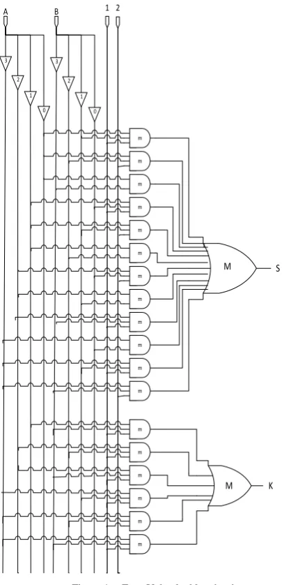
The results of these connection is shown in Fig. 1.
Step 2. AND gates: Creating an AND gate for each output instance having a value > 0.
For each input instance A0, A1, …Am-1 =x0, x1, …xm-1
that produce an output e>0, create an AND gate connecting:
Cx0(A0)·Cx1(A1)·…·Cxm-1(Am-1)·e
For e = en-1, there is no need to connect the AND gate
to e, which is the results of simplification based on the postulate P1 that is en-1·A = A.
Continuing the example of designing an adder, for the function that produce S as output (in the S column of the truth table), there are 9 instances that produce output e > 0. For example, referring to the truth table, when inputs A=0, B=1, the output S=1, in this case we create an AND gate connecting: C0(A)·C1(B)·1, in which since A=0 so
the AND gate connects to the output of C0(A) gate (from
Step 1), since B=1 so the AND gate connects to the output of C1(B) gate (from Step 1), and since S=1 so the
AND gate connects to 1. When inputs A=0, B=2, the output S=2, in this case we create an AND gate connecting: C0(A)·C2(B)·2,in which since A=0 so the
AND gate connects to the output of C0(A) gate, since
B=2 so the AND gate connects to the output of C2(B)
gate, and since S=2 so the AND gate connects to 2. And, when inputs A=0, B=3, the output S=3, in this case we create an AND gate connecting: C0(A)·C3(B)·3, which is
simplified to C0(A)·C3(B). We create 9 AND gates for
the 9 instances as shown in the below and the connections are shown in Fig. 1.
0 1 2 3
0 1 2 3
1 B
A 2
m
m
m
m
m
m
m
m
m
m
m
m
m
m
m
m
m
m
S
K M M
Figure 1. Four-Valued adder circuit
C0(A)·C1(B)·1, C0(A)·C2(B)·2, C0(A)·C3(B),
C1(A)·C0(B)·1, C1(A)·C1(B)·2, C1(A)·C2(B),
C2(A)·C0(B)·2, C2(A)·C1(B), C2(A)·C3(B)·1,
C3(A)·C0(B), C3(A)·C2(B)·1, C3(A)·C3(B)·2
Similarly, for the function that produce K as output (in the Kcolumn of the truth table), there are 6 instances that produce output e > 0. We create 6 AND gates as shown in the below and the connections are shown in Fig. 1.
C1(A)·C3(B)·1, C2(A)·C2(B)·1, C2(A)·C3(B)·1,
C3(A)·C1(B)·1, C3(A)·C2(B)·1, C3(A)·C3(B)·1
step process, implementation of any multi-valued function becomes feasible.
Step 0. Truth Table:Creating a truth table to define the multi-valued functions.
As an example, we choose to design an adder that adds two 4-valued numbers A, B. We create atruth tableto define the required functions.
Step 1. Ci(x) gates:Connecting each input x to n Ci(x)
Step 3: OR gate: Connecting the outputs of all the AND gates to an OR gate, which produces the outputs of the required function.
Finishing the example of designing an adder for the function that produce S as output (in the S column of the truth table), we connect the outputs of all the 9 AND gates (from Step 2) to an OR gate, as defined below:
S = C0(A)·C1(B)·1 + C0(A)·C2(B)·2 + C0(A)·C3(B) +
C1(A)·C0(B)·1 + C1(A)·C1(B)·2 + C1(A)·C2(B) +
C2(A)·C0(B)·2 + C2(A)·C1(B) + C2(A)·C3(B)·1 +
C3(A)·C0(B) + C3(A)·C2(B)·1 + C3(A)·C3(B)·2
Similarly, for the function that produce K as output (in the K column of the truth table), we connect the outputs of all the 6 AND gates (from Step 2) to an OR gate, as defined below:
K = C1(A)·C3(B)·1 + C2(A)·C2(B)·1 + C2(A)·C3(B)·1 +
C3(A)·C1(B)·1 + C3(A)·C2(B)·1 + C3(A)·C3(B)·1
The results all the connections are shown in Fig. 1, which is the valued circuit that implements the four-valued addition of two four-four-valued numbers.
V. DESIGNING MULTI-VALUED MEMORY
Multi-valued memory is a necessary component for designing multi-valued systems. In this section, we present our design of a D-type fuzzy flip-flop or fuzzy memory cell [32]. Our design is based on an extension of the idea of binary D flip-flop. Excitation table for binary D flip flop is shown in Table VIII. The next state Q(t+1) of a D fuzzy flip-flop is characterized as a function of both the present state Q(t)and the input state D. Min term expression for Q(t+1) is
Above equation is also referred to as the characteristic equation of the D Flip-flop. A mutually equivalent equation can be derived from Table 8 consisting of max terms
()
()
) 1
(t D Q t D Q t
Q
TABLE VIII. EXCITATION TABLE FOR BINARY DFLIP-FLOP
Above two equations can be transformed to fuzzy domain by replacing the binary operators by fuzzy operators. They can be redefined using min-max type operation and fuzzy negation as follows:
Q t D
Qt D
t
Q( 1) 1 () ()
Q t D
Q t D
t
Q( 1) 1 ( ) ( )
In which the
represents min operation and
represents max operation. These two equations, however, do not completely transform D flip-flop to the fuzzy domain. Hence, we proposed an equation that has the characteristics of both the equations and also exhibits an analogy with the binary counterpart, as follows:
D D Q t
Qt
D
t
Q( 1) ( ) 1 ( )
This equation has led to realization of the circuit of D-type fuzzy flop. The design of the new D fuzzy flip-flop is shown in Fig. 2, in which the gates are fuzzy logic AND, OR, and NOT gates. This D-type fuzzy flip-flop can be used as a fuzzy memory cell.
Figure 2. A new multi-valued memory cell
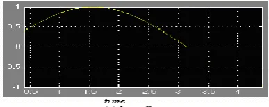
Working of the D-type fuzzy flip-flop (shown in Fig. 2) can be understood by initially considering binary values 0 or 1. If the value of the input D is set at either 0 or 1 regardless the initial value of Q at time t, Q will be set to the value of D. Any value ranging from 0 to 1 also produce the required results. To get an initial idea of the behavior of the D fuzzy flip-flop, we simulated our design using MATLAB and Simulink [33]. Fig. 3 shows the setup of the simulation and the results are shown in Fig. 4. The results show that the D fuzzy flip-flop is simply storing whatever value provided on the input D. It is simply a fuzzy memory cell.
Figure 3. Simulation setup of multi-valued memory cell using simulink
(a) Input D
) ( ) ( ) 1
(t DQt DQt
(b) Output Q
Figure 4. Simulated result of multi-valued memory cell
We extended the fuzzy memory cell to clocked D fuzzy flop. Fig. 5 shows our design of the fuzzy flip-flop. This clocked D fuzzy flip-flop can be used in the design of sequential fuzzy circuits.
Figure 5. Clocked D-type fuzzy flip-flop
VI. CONCLUSION AND FUTURE RESEARCH
Now is the time to depart from the two-valued logic to venture into multi-valued logic and even into infinite-valued or Fuzzy logic. To make multi-infinite-valued computation possible, this paper provides the necessary tools for designing multi-valued systems entirely within the domain of multi-valued logic. We describe a simple four-step process for feasible design of multi-valued circuits to implement any multi-valued function.
We also provide designs of memory cells that can store any multi-valued variable. The memory cell is the first D-type fuzzy flip-flop that can also be used as a fuzzy memory cell. We also present the circuit of a clocked D-type fuzzy flip-flop that can be used in the design of sequential fuzzy circuits. The fuzzy flip-flop is designed entire in the fuzzy domain using fuzzy AND gate, fuzzy OR gate, and fuzzy NOT gate. Thus, the realization of the flip-flop depends on the realization of the fuzzy logic gates.
The implementation of multi-valued the logic gates, including the AND, OR, NOT, and Disjoin (Ci(x)) gates,
in integrated circuits can be found in [1], [32], [34]. Thus, it would be feasible to implement the designed multi-valued circuits in integrated circuits.
Using the simple four-step process to design multi-valued circuits do not necessary provide the most simplified circuits. In most case, the circuits can further be simplified, which can be done by algebraic manipulation based on the postulates for disjoint system of Post algebras provided in Section III.
The next stage for future research will be to use the multi-valued circuit design methodology and memory cells to design large-scalecircuits for fully exploiting multi-valued logics and fuzzy paradigms in hardware.
REFERENCES
[1] B. Choi, “Advancing from two to four valued logic circuits,” in
Proc. IEEE International Conference on Industrial Technology, February 2013.
[2] P. Marinos, “Fuzzy logic and its application to switching systems,”
IEEE Transactions on Computing, vol. C-18, no. 4, pp. 343-348, Apr. 1969.
[3] L. A. Zadeh, “Fuzzy logic - computing with words,” IEEE Transactions on Fuzzy Systems, vol. 4, pp. 103-11, 1996. [4] L. A. Zadeh, “The concept of linguistic variables and its
application approximate reasoning,” Information Sciences, pp. 43-80, 1975.
[5] J. M. Mendel, “Fuzzy logic systems for engineering: A tutorial,” in Proc. IEEE, vol. 83, no. 3, March 1995.
[6] C. Isik, “Fuzzy logic: Principles, applications and perspectives,”
SAE (Society of Automotive Engineers) Transactions, vol. 100, pp. 393-396, 1991.
[7] J. W. Fattaruso, S. S. M. Shetti, and J. B. Barton, “A fuzzy logic inference processor,” IEEE Journal of Solid State Circuits, vol. 29, no. 4, pp. 397-402, Apr. 1994.
[8] G. Leslaw and J. Kluska, “Family of fuzzy J-K flip-flops based on bounded product, bounded sum and complementation,” IEEE Transactions on Systems, Man, and Cybernetics, Part B: Cybernetics, vol. 28, no. 6, pp. 861-868, Dec. 1998.
[9] N. H. E. Weste and K. Eshraghian, Principles of CMOS VLSI Design, Addison-Wesley Publishing Company, 1994, pp. 61-69. [10] R. J. Baker, CMOS Circuit Design, Layout, and Simulation, 2nd
ed. B. R. Jacob, 1964.
[11] V. Catania, A. Puliafito, M. Russo, L. Vita, “A VLSI fuzzy inference processor based on a discrete analog approach,” IEEE Transactions on Fuzzy Systems, vol. 2, no. 2, pp. 93-106, May 1994.
[12] G. Ascia, V. Catania, and M. Russo, “VLSI hardware architecture for complex fuzzy systems,” IEEE Transaction on Fuzzy Systems, vol. 7, no. 5, pp. 553-570, Oct. 1999.
[13] G. Ascia and V. Catania, “A high performance processor for application based on fuzzy logic,” in Proc. Fuzzy Systems Conference, vol. 3, Aug. 22-25, 1999, pp. 1685-1690.
[14] T. Yamakawa, T. Inoue, F. Ueno, and Y. Shirai; “Implementation of fuzzy logic hardware systems-three fundamental arithmetic circuits,” Trans. Inst. Electron Common. Eng. Japan, vol. J63-C, no. 10. pp. 720-721, Oct. 1980.
[15] K. Hirota, “Fuzzy logic and its hardware implementation,” in
Proc. 2nd New Zealand Two-Stream International Conference on Artificial Neural Networks and Expert systems, 1995, pp. 102. [16] J. L. Perez and M. A. Banuloes, “Electronic model on fuzzy gates,”
Journal of the Mexican Society of Instrumentation, vol. 3, pp. 43-46, 1995.
[17] V. Catania and M. Russo, “Analog gates for a VLSI fuzzy processor,” in Proc. 8th International Conference of VLSI Design, Jan. 1995.
[18] K. Ozawa, K. Hirota, L. T. Koczy, W. Pedrycz, and N. Ikoma, “Summary of fuzzy flip-flop,” in Proc. International Joint Conference of the 4th IEEE International Conference on Fuzzy Systems and the 2nd International Fuzzy Engineering Symposium, 1995, pp. 1641-1648.
[19] K. Hirota and K. Ozawa, “The concept of fuzzy flip-flop,” IEEE Transactions on Systems, Man and Cybernetics, vol. 19, no. 5, pp. 980-997, 1989.
[20] K. Hirota and W. Pedrycz, “Designing sequential systems with fuzzy J-K flip-flops,” Fuzzy Sets and Systems, vol. 39, no. 3, pp. 261, Feb. 15, 1991.
[23] K. Hirota and W. Pedrycz, “Design of fuzzy systems with fuzzy flip-flops,” IEEE Transactions on Systems, Man and Cybernetics, vol. 25, no. 1, pp. 169-176, Jan 1995.
[24] J. Virant, N. Zimic, and M. Mraz, “T-type fuzzy memory cells,”
Fuzzy Sets and Systems, vol. 102, no. 2, pp. 175-183, Mar. 1, 1999.
[25] S. M. Kia and S. Parmeswaran, “Designs for self checking flip-flops,” IEE Proceedings: Computers and Digital Techniques, vol. 145, no. 2, pp. 81-88, Mar. 1998.
[26] T. Miki and T. Yamakawa, “Fuzzy inference on an analog fuzzy chip,” IEEE Micro, pp. 8-18, 1995.
[27] T. Kettner, C. Heite, and K. Schumacher, “Analog CMOS realization of fuzzy logic membership functions,” IEEE Journal of Solid State Circuits, vol. 28, no. 7, pp. 857-886, Jul. 1993. [28] H. Watanabe, W. D. Dettloff, and K. E. Yount, “A VLSI fuzzy
logic controller with reconfigurable, cascadable architecture,”
IEEE Journal of Solid-State Circuits, vol. 25, pp. 376-382, Apr. 1990.
[29] D. De Venuto, M. J. Ohletz, and B. Ricco, “Testing of analogue circuits via (standard) digital gates,” in Proc. International Symposium on Quality Electronic Design, Mar. 18-21, 2002, pp. 112-119.
[30] I. Baturone, A. Barriga, S. Sanchez-Solano, and D. R. Lopez,
Microelectronic Design of Fuzzy Logic-Based Systems, CRC Press, 2000.
[31] G. Epstein, Multiple-Valued Logic Design: An Introduction, Institute of Physics Publishing, 1993.
[32] B. Choi and K. Tipnis, “New components for building fuzzy logic circuits,” in Proc. Fourth International Conference on Fuzzy Systems and Knowledge Discovery, vol. 2, 2007, pp. 586-590. [33] “Simulink: Simulation and model based design,” Version 6, The
Mathworks, 2005.
[34] G. Wu, L. Cai, and Q. Li, “Ternary logic circuit design based on single electron transistors,” Journal of Semiconductors, vol. 30, no. 2, Feb. 2009.
Dr. Ben Choi has a Ph.D. degree in Electrical and Computer Engineering and also has a Pilot certificate for flying airplanes and helicopters. He is an Associate Professor in Computer Science at Louisiana Tech University. He received his Ph.D., M.S., and B.S. degrees from The Ohio State University, studied Computer Science, Computer Engineering, and Electrical Engineering. His areas of research include Humanoid Robots, Artificial Intelligence, Machine Learning, Intelligent Agents, Semantic Web, Data Mining, Fuzzy Systems, and Parallel Computing. His future research includes developing advanced software and hardware methods for building intelligent machines and theorizing the Universe as a Computer.
Kankana Shukla is a Masters student in C o m p u t e r S c i e n c e a n d B i o m e d i c a l Engineering at Louisiana Tech University. She completed her bachelors in Electronics and Instrumentation. Her research interest includes Data Mining, Web Mining, Big D a t a A n a l y s i s , M a c h i n e L e a r n i n g , Bioinformatics, Biostatistics, Robotics and Artificial Intelligence. Her future work includes pursuing a Ph.D. degree in Data Mining and Biostatistics.