Bilinear Interpolation Image Scaling Processor for VLSI
Ms. Pawar Ashwini Dilip M. E. (Electronics)., KBPCE, Shivaji University,
Mh.S.
Dr. K. Rameshbabu Dean (Academics) & Prof.,
JCEM, Shivaji University, Mh.S.
Ms. Shital Arjun Shivdas M.E (VLSI & ES)., ADCET, Shivaji University,
Mh.S.
Ms. Kanase Prajakta Ashok B.E (E & TC),
RIT, Shivaji University, Mh.S.
Abstract – We introduce image scaling processor using VLSI technique. It consist of Bilinear interpolation, clamp filter and a sharpening spatial filter. Bilinear interpolation algorithm is popular due to its computational efficiency and image quality. But resultant image consist of blurring edges and aliasing artifacts after scaling. To reduce the blurring and aliasing artifacts sharpening spatial filter and clamp filters are used as pre-filter. These filters are realized by using T-model and inversed T-model convolution kernels. To reduce the memory buffer and computing resources for proposed image processor design two model or inversed T-model filters are combined into combined filter which requires only one line buffer memory. Also, to reduce hardware cost Reconfigurable calculation unit (RCU)is invented. The VLSI architecture in this work can achieve 280 MHz with 6.08-K gate counts, and its core area is 30 378μm2 synthesized by a 0.13-μm CMOS process.
Keywords – Bilinear, Clamp Filter, Reconfigurable Calculation Unit (RCU), T-Model, Sharpen, Spatial Filter, VLSI.
I. I
NTRODUCTIONIn many applications, from consumer electronics to medical imaging image scaling algorithm can be used to improve the restructured image quality and processing performance of hardware implementation. For example image scaling is can be used to scale down the high-quality pictures or video frames to fit the mini size liquid crystal display panel of the mobile phone or tablet PC or a video source with a 640×480 video graphics array (VGA) resolution may need to fit the 1920×1080 resolution of a high-definition multimedia interface (HDMI).Image scaling algorithm has two main type polynomial based and non polynomial based.
In the most basic case, the fractional part of any sub pixel address is truncated or rounded, so each pixel simply takes the value of the nearest “real” pixel in the source image. This is called “nearest neighbor” approximation. This method is the simplest, and involves no calculation. It also only requires one pixel from the source image for each sub pixel which is being calculated; hence it can operate at the full speed of the surrounding circuit. However, the resultant approximation is not optimal with this technique.
Bilinear interpolation method has high quality and low complexity. By using bilinear interpolation algorithm the target pixel can be obtained by using the linear interpolation model in both of the horizontal and vertical directions.Bicubic interpolation is often chosen over bilinear interpolation or nearest neighbor in image resampling, when speed is not an issue. It is another popular method uses an extended cubic model to acquire the target pixel by a 2-D regular grid.
In our previous work , an adaptive real-time, low-cost, and high-quality image scalar was proposed. It successfully improves the image quality by adding sharpening spatial and clamp filters as pre filters with an adaptive technique based on the bilinear interpolation algorithm. Although the hardware cost and memory requirement had been efficiently reduced, the demand of memory still costs four line buffers. Hence, a low-cost and low memory-requirement image scalar design is proposed in this brief.
Table I compares the computing resources and memory access per pixel of four well-known interpolation algorithms. The bilinear interpolation algorithm demands low computing resource and memory access per pixel. However, it causes the edges of the scaled images to become blurred and aliased after interpolation. Kim et al. presented an area-pixel model called the “Win scale” algorithm. It uses a maximum of four pixels of the original image to calculate one pixel of a scaled image. In addition, Andreadis et al. Proposed a modified Win scale algorithm that uses a mask of no more than four pixels and calculates the final luminosity of each pixel to scale grey-scale and color images. This method offers better quality than the Win scale algorithm. However, it requires more computing resources than does the Win scale algorithm.
Table I: Comparison Of Computingresource & Memory Access/Pixel Of Four Interpolation Algorithms
Bi linear
Win scale
M-Winscale
Bicubic
Computing Resources
7Mult 7add
10Mult 11add
13Mult 20add
32Mult 53add Memory
Access
4 read 1 write
4 read 1 write
4 read 1 write
4 read 16 write
This paper is organized as follows. In Section II, the bilinear interpolation, clamp filter, and sharpening spatial filter are briefly introduced.
between these two points. Figure 2 shows how this is done for an image. In each case, the linear interpolation between two values a and b by fraction k is computed as (b - a) X k+a.Bilinear interpolation offers significantly enhanced image quality over Nearestneighbor approximation. Bilinear nterpolation is an image-restoring algorithm, which linearly interpolates four nearest-neighbor pixels of an unrestored image to obtain the pixel of a restored image as a forward function. The principle behind the bilinear interpolation algorithm is executing a linear interpolation in one direction, and then repeating the same function in the other direction. As shown in Fig. 2, P(i, j), P(i+1,j), P(i,j+1), and P(i+1,j+1) are the four nearest neighbor pixels of the original image with i = [0, 1, 2, . . . M] and j = [0, 1, 2, . . . N]. Here, M is the number of pixels having the width of the original image and N is the number of pixels corresponding to the length of the original image.The temporary pixels P(x’,j) and P(x’,j+1) are
created by linear interpolation in horizontal direction and can be calculated as
P(x’, j)= (1−xf ) × P(i, j) + xf × P(i+1, j) (1.1)
P(x’, j+1) = (1−xf ) × P(i, j+1) + xf × P(i+1, j+1) (1.2) where xf is the scale parameter in horizontal direction. After interpolating in horizontal direction, the values of temporary pixels P(x’,j) and P(x’,j+1) are generated. The resulting output pixel P(x’,y’) can be obtained by one more linear interpolation in the other direction. Alternatively, the output can be produced by implementing linear interpolation in the vertical direction and can be calculated as
P(x’, y’) = [(1 − xf ) × P(i, j) + xf× P(i+1, j)] × (1− yf ) +[(1− xf ) × P(i, j+1) + xf× P(i+1, j+1)] ×yf
(1.3) where yf is the scale parameter in vertical direction. Bilinear interpolation is popular in the implementation of VLSI chips due to its low complexity and simple architecture. However, its high-frequency response behavior is poor as a result of linear changes to the output pixel value according to sampling position. Results show that the edges become blurry and the aliasing effect is visible after being processed using bilinear interpolation.
Fig.2. Bilinear interpolation grid.
Given a point (x,y),We interpolate between floor (x) and ceil(x) on each of two rows floor(y) and ceil(y)using fractional part of x to obtain two intermediate points shown .then we use fractional part of y to interpolate between these two points to obtain final interpolated value.
By (1.1),We can easily find that the computing resources of the bilinear cost eight multiply, four subtract, and three addition operations. It costs a considerable chip area to implement a bilinear interpolator with eight multiplies and seven adders. Thus, an algebraic manipulation skill has been used to reduce the computing resources of the bilinear interpolation. The original equation of bilinear interpolation is presented in (1.1),and simplified procedure of bilinear interpolation can be described from (1.2)-(1.3),one of the two calculations for this algebraic function can be reduced
P(x’, y’)=[ (1−yf ) × P(i+1, j) + yf ×P(i+1, j+1)] xf +[(1−yf) × P(i, j)+ yf × P(i, j+1)] (1−xf)
(1.4) = [P(i+1, j) + yf P(i+1, j+1)- P(i+1, j)]xf +
[P(i, j)+yf × P(i, j+1) - P(i, j)](1−xf)
(1.5)
I.2 Low-Complexity Sharpening Spatial and Clamp
Filters:
The sharpening spatial filter, a kind of high-pass filter, is used to reduce blurring artifacts and defined by a kernel to increase the intensity of a center pixel relative to its neighboring pixels. It usually contains a single positive value at its center and completely surrounded by negative values. The following array is an example of a 3 × 3 kernel for a sharpening spatial filter
1 1 1
1 1
1 1 1
S Kernel
Where S is a sharp parameter that can be set according to the characteristics of the images. The clamp filter is a kind of low-pass filter, is used to smooth unwanted discontinuous edges of boundary regions and reduce aliasing effects. It can be represented by a convolution kernel.
1 1 1
1 1
1 1 1
S Kernel
Here, C is a clamp parameter that can be set according to the characteristics of the images.
(a)
(c)
Fig.3. Weights of the convolution kernels. (a) 3 × 3 convolution kernel. (b) Cross-model convolution kernel.
(c) T-model and inversed T-model convolution kernels. This kernel is combined with matrix coefficients that show the dependence of a filtered pixel on its neighbors. A larger size of convolution kernel will produce higher quality of images. However, a larger size of convolution filter will also demand more memory and hardware cost. To reduce the complexity of the 3 × 3 convolution kernel, a cross-model formed is used to replace the 3 × 3 convolution kernel, as shown in Fig. 3(b). It successfully cuts down on four of nine parameters in the 3 × 3 convolution kernel. Furthermore, to decrease more complexity and memory requirement of the cross-model convolution kernel, T-model and inversed T-model convolution kernels are proposed for realizing the sharpening spatial filter and clamp filters.
I.3. Combined Filter:
In proposed scaling algorithm to reduce more computing resource and memory requirement spatial and clamp filter which formed by T-model and Inversed T-model should be combined together into combined filter. The input image is filtered by sharpening spatial filter and then filtered by clamp filter again. Both filters requires two line buffer to store input data or intermediate value for each T model or inversed T model. Due to this these two filters combined together into combined filter asWhere S and C are the sharp and clamp parameters and P’(i,j) is the filtered result of the target pixel P(i,j) by the combined filter. A T-model sharpening spatial filter and a model clamp filter have been replaced by a combined T-model filter as shown in Fig.3 To reduce the one-line-buffer memory, the only parameter in the third line, parameter −1 of P(i,j-2),is removed and the weight of parameter−1 is added into the parameter S-C of P(i,j-1) by S-C-1 as shown in (2). The combined inversed T-model filter can be produced in the same way. The demand of memory can be efficiently decreased from two to one line buffer by using this filter-combination technique. In this two T-model or inversed T-model filters are combined into one combined T-model or inversed T-model filter. It greatly reduces memory access requirements for software systems or hardware memory costs for VLSI implementation.
I.4 VLSI Architecture:
For VLSI implementation, the bilinear interpolator can directly obtain two input pixels P’(i,j), and P’(i,j+1) from twocombined prefilters without any additional line-buffer memory.Fig.4. Block diagram of the VLSI architecture for proposed real-time image scaling processor Fig. 4 shows the block diagram of the VLSI architecture for the proposed design. It consists of four main blocks: a register bank, a combined filter, a bilinear interpolator, and a controller. The details of each part will be described in the following sections.
The combined filter is filtering to produce the target pixels of P’(i,j), and P’(i,j+1) by using ten source pixels. The register bank is designed with a one-line memory buffer, which is used to provide the ten values for the immediate usage of the combined filter.
Fig.5. Architecture of the register bank.
Fig.5 shows the architecture of the register bank with a structure of ten shift registers. When the shifting control signal is produced from the controller, a new value of P(i+3,j) will be read into Reg41, and each value stored in other registers belonging to row n + 1 will be shifted right into the next register or line-buffer memory. The Reg 40 reads a new value of P(i+2,j) from the line-buffer memory, and each value in other registers belonging to row n will be shifted right into the next register.
It shortens the delay path to improve the performance by pipeline technology. In fig.6 stages1 and 2 show the computational scheduling of a T-model combined and an inversed T-model filter. The T-model or inversed T-model filter consists of three reconfigurable calculation units (RCUs), one multiplier–adder (MA), three adders (+), three subtracters (−), and three shifters (S). The hardware architecture of the T-model combined filter can be directly mapped with the convolution equation shown in (1.2). The values of the ten source pixels can be obtained from the register bank .
The symmetrical circuit, as shown in stages 1 and 2 of Fig. 6, is the inversed T-model combined filter designed for producing the filtered result of P’(i,j+1) The architecture of this symmetrical circuit is a similar symmetrical structure of the T-model combined filter, as shown in stages 1 and 2 of Fig. 6. Both of the combined filter and symmetrical circuit consist of one MA and three RCUs. The MA can be implemented by a multiplier and an adder. The RCU is designed for producing the calculation functions of (S-C) and (S-C-1) times of the source pixel value, which must be implemented with C and S parameters.
Fig.7. Architecture of the RCU
The architecture of the proposed low-cost combined filter can filter the whole image with only a one-line-buffer memory, which success fully decreases the memory requirement from four to one line buffer of the combined filter in our previous work . Table I lists the parameters and computing resource for the RCU. With the selected C and S values listed in Table I, the gain of the clamp or sharp convolution function is {8, 16, 32} or {4, 8, 16}, which can be eliminated by a shifter rather than a divider.
Table I: Parameters and Computing Resource For RCU Parameter Values Computing Resources
s 5,13,29 Add and Shift
c 7,11,19 Add and Shift
s-c 2,-6,-22,6,-2,-18,14,6,-10
Add, Shift and sign s-c-1
1,-7,-23,5,-3,-19,13,5,-11
Add, Shift and sign
It consists of four shifters, three multiplexers (MUX), three adders, and one sign circuit. By this RCU design, the hardware cost of the combined filters can be efficiently reduced.
The bilinear interpolation is simplified as shown in fig 1.3. The stages 3, 4, 5, and 6 in Fig.6 show the four-stage pipelined architecture, and two-stage pipelined multipliers are used to shorten the delay path of the bilinear
interpolator. The input values of P’(i,j) and P’(i,j+1) are obtained from the combined filter and symmetrical circuit. By the hardware sharing technique, as shown in (1.3) The controller is implemented by a finite-state machine circuit. It produces control signals to control the timing and pipeline stages of the register bank, combined filter, and bilinear interpolator.
II. S
IMULATIONR
ESULTS ANDC
HIPI
MPLEMENTATIONTo be able to analyze the qualities of the scaled images by various scaling algorithms, a peak signal-to-noise ratio (PSNR) is used to quantify a noisy approximation of the refined and the original images. Since the maximum value of each pixel is 255, the PSNR expressed in dB can be calculated as
where M and N are the width and height of the original image. Four well-known scaling algorithms, Winscale (Win), modified Winscale (M−Win), bicubic (BC) , and bilinear (BL), and each step of the proposed adaptive scaling algorithm are used to analyze the qualities of each algorithm by using the eight testing images.
Fig.8. Eight sample images in the test set. (a) Lena. (b) Peppers. (c) Airplane. (d) Mandrill.
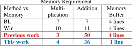
work. According to Table III, this work needs only four multiplication operations, which is much less than 7, 10, 32, or 13 in bilinear , Win , BC , or Edge-Oriented , respectively.
The VLSI architecture of this work was implemented by using the hardware description language Verilog. The
electronic design automation tool Design Vision has been used to synthesize the VLSI Circuit based on Taiwan Semiconductor Manufacturing Company 0.18-μm and 0.13-μm process standard cells.
Table II: Comparisons of Average PSNR for Various Scaling Algorithms
BL Win BC Edge Ada This Work
A B C
Half 27.04 27.30 28.5 27.42 28.49 27.68 27.77 28.27
CIF 27.8 27.75 28.7 27.82 29.45 27.68 27.83 28.27
VGA 28.5 28.55 28.7 28.58 29.44 28.39 28.42 28.22
DI 28.5 28.51 28.92 28.55 29.44 28.54 28.45 28.61
DOU 28.5 28.52 28.92 28.58 29.37 28.56 28.8 28.78
HDMI 28.56 26.94 28.97 26.96 29.38 27.87 28.66 28.76
AVE 28.15 27.93 28.96 27.99 29.2 28.29 28.32 28.54
A: Using Sharp filter and bilinear interpolation, B: Using clamp filter and bilinear interpolation, C: Using combined filter and bilinear interpolation.
Table III: Comparison of Computing Resource and Memory Requirement
Method vs Memory
Multi-plication
Addition Memory Buffer
BL 7 7 4 lines
Win 10 11 4 lines
Previous work 3 50 4 lines
This work 4 36 1 line
The layout for the proposed design was generated with IC Compiler. The chip photomicrograph is illustrated in Fig. 7. Furthermore, the proposed design was evaluated and verified by an field programmable gate array (FPGA) emulation board with an Altera FPGA EP2C70F896C6 core. This work contains only 6.08-K gate counts, and the chip area is 30 378μm2 synthesized by a 0.13-μm CMOS process. Moreover, this work can process the whole image with only a one-line-buffer memory. The power consumption of the proposed design was measured by using SYNOPSYS Prime Power. It consumes 6.9 mW at a 280-MHz operation frequency with a 1.1-V supply voltage. Furthermore, the throughput of this work achieves 280 megapixels per second. It is fast enough to achieve the demand of real-time graphic and video applications with a HDMI of WQSXGA (3200 × 2048) resolution at 30 frames per second.
Fig.9. Chip photomicrograph
III. C
ONCLUSIONIn this paper efficient and low memory VLSI architecture of bilinear interpolator and combined filter was presented for image scaling application. This method consist of three steps such as filtering of images using clamp and spatial 2D filter, bilinear interpolation and VLSI implementation. The computational complexity of function is decreased by combined filter and algebraic manipulation of the bilinear interpolation. Comparing with other low complexity architecture this work achieves at least 34.5% reduction in gate counts and requires only one-line memory buffer.
R
EFERENCES[1] S. L. Chen, H. Y. Huang, and C. H. Luo, “A low-cost high-quality adaptive scalar for real-time multimedia applications,” IEEE Trans. Circuits Syst. Video Technol., vol. 21, no. 11, pp. 1600–1611, Nov. 2011.
[2] F. Cardells-Tormo and J. Arnabat-Benedicto, “Flexible hardware-friendly digital architecture for 2-D separable convolution-based scaling,”IEEE Trans. Circuits Syst. II, Exp. Briefs, vol. 53, no. 7, pp. 522–526, Jul. 2006.
[3] S. Ridella, S. Rovetta, and R. Zunino, “IAVQ-interval-arithmetic vector quantization for image compression,” IEEE Trans. Circuits Syst. II, Analog Digit. Signal Process., vol. 47, no. 12, pp. 1378–1390, Dec. 2000.
[4] H. Kim, Y. Cha, and S. Kim, “Curvature interpolation method for image zooming,”IEEE Trans. Image Process., vol. 20, no. 7, pp. 1895–1903, Jul. 2011
[5] J. W. Han, J. H. Kim, S. H. Cheon, J.O.Kim, and S. J. Ko, “Anovel image interpolation method using the bilateral filter,” IEEE Trans. Consum. Electron., vol. 56, no. 1, pp. 175–181, Feb. 2010.
[6] X. Zhang and X.Wu, “Image interpolation by adaptive 2-D autoregressive modeling and soft-decision estimation,” IEEE Trans. Image Process., vol. 17, no. 6, pp. 887–896, Jun. 2008. [7] K. Jensen and D. Anastassiou, “Subpixel edge localization and
the interpolationof still images,”IEEE Trans. Image Process., vol. 4, no. 3, pp. 285–295, Mar. 1995.
[9] P. Y. Chen, C. Y. Lien, and C. P. Lu, “VLSI implementation of an edge oriented image scaling processor,” IEEE Trans. Very Large Scale Integr. (VLSI) Syst., vol. 17, no. 9, pp. 1275–1284, Sep. 2009.
[10] C. C. Lin, M. H. Sheu, H. K. Chiang, W. K. Tsai, and Z. C. Wu, “Real-time FPGA architecture of extended linear convolution for digital image scaling,” inProc. IEEE Int. Conf. Field-Program. Technol., 2008, pp. 381–384.
A
UTHOR’SP
ROFILEMiss. Pawar Ashwini Dilip
B.E. (Electronics), M.E. (Electronics)., K.B.P. College of Enginering 2012, 14 respectively Satara. Area of Interest: VLSI Design, Embedded system. Software Known: Xilinx10.1, MATLAB11, Keil, Turbo C, Microwind.
Work Experience: 3Ys as Assistant Professor in Jaywant College of Engg and Management, K.M.Gad (2010-2013). Hobbies: Drawing, Reading Novels.
Languages: Hindi, Marathi, English.
Dr. K. Ramesh babu
Professor & Dean (academics), E & TC, JCEM, karad Mh.S. he is holding B.E (ece), M.Tech, Ph.D. having 17+ years of experience in electronics and Telecommunication Engineering area. He is member in ISTE, IEEE & Java Certified programmer (2,0) PGDST holder. he has lot of experience in academics and industrial related realtime projects. He is paper setter for many autonomous universities and also visiting professor for subjects like image processing, electron devices & communications etc.
Shital Arjun Shivdas
B.E. (E & TC), Annasaheb Dange college of Engg. Ashta in 2012, M.E. (VLSI & Embedded System)., ADCET. Interested in Lab operations & research work.
Area of Interest: Embedded system, Digital Design, VLSI Design.
Softwares Known: Xilinx10.1, MATLAB11, Keil,Turbo C, Microwind. Work Experience: 1Y as Assistant Professor in Jaywant College of Engg and Management, K. M. Gad (2010-2013).
Hobbies: Reading Novels, Meditation. Languages: Hindi, Marathi, English.
Miss. Kanase Prajkta Ashok
B.E. (E & TC), RIT, Sakharale 2012,Area of Interest: VLSI Design, Digital Communication,
Software Known: Xilinx10.1, MATLAB11, Keil, Turbo C, Microwind.
Work Experience: 2 Yrs as Assistant Professor in Jaywant College of Engg and Management.