Middlesex University Research Repository
An open access repository of
Middlesex University research
http://eprints.mdx.ac.uk
Langlois, Peter J., Wu, Yu, Bayford, Richard and Demosthenous, Andreas (2015) On the application of frequency selective common mode feedback for multifrequency EIT. Physiological
Measurement, 36 (6). pp. 1337-1350. ISSN 0967-3334
Published version (with publisher’s formatting)
This version is available at:http://eprints.mdx.ac.uk/15812/
Copyright:
Middlesex University Research Repository makes the University’s research available electronically.
Copyright and moral rights to this work are retained by the author and/or other copyright owners unless otherwise stated. The work is supplied on the understanding that any use for commercial gain is strictly forbidden. A copy may be downloaded for personal, non-commercial, research or study without prior permission and without charge.
Works, including theses and research projects, may not be reproduced in any format or medium, or extensive quotations taken from them, or their content changed in any way, without first obtaining permission in writing from the copyright holder(s). They may not be sold or exploited commercially in any format or medium without the prior written permission of the copyright holder(s).
Full bibliographic details must be given when referring to, or quoting from full items including the author’s name, the title of the work, publication details where relevant (place, publisher, date), pag-ination, and for theses or dissertations the awarding institution, the degree type awarded, and the date of the award.
If you believe that any material held in the repository infringes copyright law, please contact the Repository Team at Middlesex University via the following email address:
The item will be removed from the repository while any claim is being investigated.
This content has been downloaded from IOPscience. Please scroll down to see the full text.
Download details:
IP Address: 158.94.123.241
This content was downloaded on 15/04/2016 at 15:51
Please note that terms and conditions apply.
On the application of frequency selective common mode feedback for multifrequency EIT
View the table of contents for this issue, or go to the journal homepage for more 2015 Physiol. Meas. 36 1337
1337 Physiological Measurement
On the application of frequency
selective common mode feedback for
multifrequency EIT
Peter J Langlois1, Yu Wu1, Richard H Bayford2 and
Andreas Demosthenous1
1 Department of Electronic and Electrical Engineering, University College London,
London, WC1E 7JE, UK
2 Department of Natural Sciences, Middlesex University, The Burroughs, London,
NW4 4BT, UK
E-mail: [email protected]
Received 6 January 2015, revised 6 February 2015 Accepted for publication 10 February 2015 Published 26 May 2015
Abstract
Common mode voltages are frequently a problem in electrical impedance tomography (EIT) and other bioimpedance applications. To reduce their amplitude common mode feedback is employed. Formalised analyses of both current and voltage feedback is presented in this paper for current drives. Common mode effects due to imbalances caused by the current drives, the electrode connections to the body load and the introduction of the body impedance to ground are considered. Frequency selective narrowband common mode feedback previously proposed to provide feedback stability is examined. As a step towards multifrequency applications the use of narrowband feedback is experimentally demonstrated for two simultaneous current drives. Measured results using standard available components show a reduction of 62 dB for current feedback and 31 dB for voltage feedback. Frequencies ranged from 50 kHz to 1 MHz.
Keywords: bioimpedance, common mode error, common mode feedback, current drive, imbalance, multifrequency
(Some figures may appear in colour only in the online journal)
P J Langlois et al
Printed in the UK
1337
Pmea
© 2015 Institute of Physics and engineering in medicine 2015
36
Physiol. meas.
Pmea
0967-3334
10.1088/0967-3334/36/6/1337
Special issue papers (internally/externally peer-reviewed)
6
1337
1271
Physiological measurement
Institute of Physics and Engineering in Medicine
Content from this work may be used under the terms of the Creative Commons Attribution 3.0 licence. Any further distribution of this work must maintain attribution to the author(s) and the title of the work, journal citation and DOI.
0967-3334/15/061337+14$33.00 © 2015 Institute of Physics and Engineering in Medicine Printed in the UK
1. Introduction
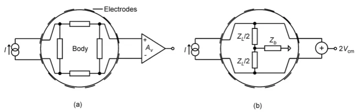
The established method of electrical impedence tomography (EIT) (Boone and Holder 1996, Bayford 2006) uses an array of sensing electrodes as shown in figure 1(a). The body is a non-uniform conducting medium. Current is injected into two electrodes and the voltage across pairs of electrodes is detected and amplified. Algorithms using the resulting voltage measure-ments deduce the disposition of different components in the body (Bayford 2006, Adler et al
2009). Measurements from a current drive with simultaneous multiple frequencies are also employed (McEwan et al2007). Increasing the number of electrodes and employing drives with more than one sinewave frequency enable better definition of the body components. When there are a large number of electrodes the voltages across the distant sense electrodes due to the current drive can be very small. The amplitude of the differential voltages depends on the application, but voltages down to about 0.05 mV can be expected.
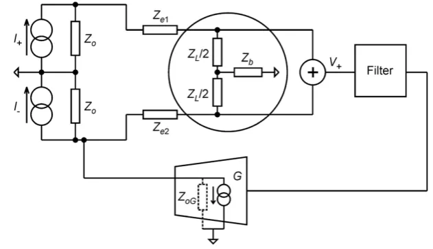
Current drives are generally floating, i.e. have high impedance to ground, to provide an optimal regime to enable sense amplifiers to detect very small differential signals. In fig-ure 1(a) to aid analysis the distributed nature of the body has been simplified to an equivalent circuit containing four impedances (Rosell and Rui 1992). These represent the attenuation of the differential signals between the drive electrodes and the sense electrodes.
Any mismatch or imbalance particularly in the driving circuit or contact electrodes gen-erates a common mode signal at the same frequency as the differential signal which has to be accommodated by the sense amplifier. Due to the high output impedance of the current drive (Bertermes-Filho et al2000, Ross et al2003, Hong et al2009), common mode signals of around 0.5 V are possible and would require a common mode rejection ratio (CMRR) of between 140 dB and 107 dB for 0.1% accuracy of the measurement (Rosell and Rui 1992, Boone and Holder 1996). The high CMRR required of the sense amplifier can be reduced by applying common mode feedback before the sense amplifier input. Mismatches in the sense amplifier will also cause unwanted common mode signals but are not considered here. The common mode voltage experienced at the electrodes is assumed to be the same on all electrodes which for common mode signals allows the circuit to be further simplified to figure 1(b). In this figure the effect of the body impedance to ground, Zb, has been added as a centre tap which
assumes that Zb does not cause mismatch. There is always a Zb component either through body
capacitance to earth and/or a reference electrode but provision of a reference electrode in an EIT system can distort the field distribution being monitored and may be undesirable. The common mode voltage Vcm is derived by adding the voltages on two sense electrodes (=2Vcm).
This paper formalises the analysis, which previously has not been explicitly addressed, of com-mon mode effects due to imbalances caused by current drives, mismatch of electrode connections and the effect of the body impedance to ground. It also examines the introduction of narrowband common mode feedback to address problems of stability encountered in conventional wideband EIT feedback systems. In section 2 the analysis and comparison of the application of common mode current or voltage feedback is discussed. Section 3 introduces narrowband common mode feedback and its transient response. Section 4 presents measured results of dual frequency current and voltage feedback. Section 5 discusses the results and conclusions are in section 6.
2. Common mode feedback
2.1. Feedback options
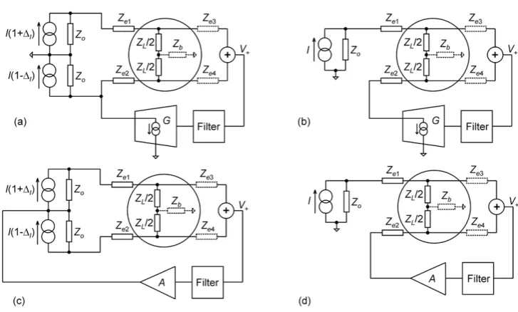
feedback options. Components Ze have been added to represent the electrode contact imped-ances and the ideal floating current drive in figure 1 has been replaced by the practical realiza-tion of two balanced current drives (figures 2(a) and (c)).
Common mode feedback can use either voltage feedback or current feedback (Hwang
2005, Hwang and Park 2005). Referring to figure 2, the options shown are:
(a) ‘Balanced’ current drive using current feedback to the electrode Ze2. In practice there is
always a small mismatch ΔI of the two current drives.
(b) Single current drive using current feedback. The balancing current is supplied by the feedback transconductor G. This is a simpler version of option (a) and the feedback loop gain required is much higher.
(c) Centre tapped feedback (Casas et al1996, Anton and Riu 2010). Voltage feedback A is connected to the centre tap of the ‘balanced’ current drive.
(d) Single current drive using voltage feedback. The balance current is supplied by A. The feedback loop gain must be much higher compared with (c).
The filter defines the frequency characteristics of the feedback loop.
2.2. Feedback options
Using the example of figure 2(a) for balanced drive when there is no feedback and assuming
Zo >> Ze the common mode voltage Vcm is
Δ
= ++
V IZ Z Z Z
Z Z Z
( /2) 2
I o L o b
o o b
cm
(1)
where Zo is the output impedance of each of the ‘balanced’ current drives and ΔII is their mismatch error. The effect of the value of Zb on the common mode voltage is illustrated by considering the extreme cases:
Δ Δ
= ∞ = = =
Z V IZ Z V IZ
For ; for 0
2 .
b cm I o b cm I L
(2)
Since Zo >> ZL when there is no feedback the common mode voltage can be significantly reduced by a low value of Zb.
The common mode voltage can be reduced by applying current feedback as in figure 2(a). The common mode voltage is then (see appendix A)
Δ = + + + + + V IZ GZ 1 . I o
Z Z Z
Z Z Z
oZZ Z ZZ Z
cm
( / 2) 2
( / 2) 2
L o b
o o b
L o b
o o b
(3)
For extreme values of Zb (3) can be simplified to:
Δ Δ
= ∞ =
+ = = +
Z V I Z
GZ Z V I
Z GZ For
1 ; for 0
/2
1 /2.
b I o
o b I
L
L
cm cm
(4)
If GZo and GZL/2 >> 1 both equations in (4) simplify to
Δ ≈ V I G . I cm (5)
A similar analysis of the voltage feedback option in figure 2(d) (assuming Ze = 0) yields
= +
+
(
+)
V I Z Z Z
A 2
( /2) ( /2)
1 1 .
L L b
Z Z Z cm o b o (6)
For extreme values of Zb (6) can be simplified to:
= ∞ =
+ = = +
Z V IZ
A Z V
IZ A For
2 1
1 2 ; for 0 4
1
1 .
b cm L b cm L
(7)
If A >> 1 both equations in (7) simplify to
= V IZ A 4 . L cm (8)
Figure 2. Common mode equivalent circuits of current drive EIT systems with different feedback options. V+= 2Vcm. (a) ‘Balanced’ current drive, current feedback;
(b) Single current drive, current feedback; (c) ‘Balanced’ current drive, centre tapped voltage feedback; (d) Single current drive voltage feedback. It is assumed that the effect of Ze3 and Ze4 can be ignored because the adder has high input impedance. Analyses of
In (4) and (7) when the loop gain is sufficiently large the common mode voltage has been reduced to a value independent of Zb. Similar results occur in the other two options in figure 2.
2.3. Stability
The stability of the feedback is identified by the phase margin at the frequency when the feed-back loop gain is unity. From (4) the current feedfeed-back loop gains AL are:
= ∞ ∞= = =
Z A GZ Z A GZ
For b L o; for b 0 L0 L.
(9)
Since GZo or GZL will have more than one pole and Zo >> ZL the low frequency gain of ∞
AL is high and there will be more instability compared with AL0. The loop gain variation in
(7) is far less than (4). If there are wide variations in ZL and Zb, introduction of a dominant pole to ensure stability must be based on the worst case values expected. The dominant pole affects the settling time.
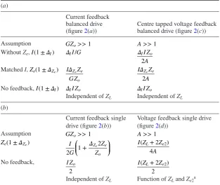
2.4. Comparison of feedback options
Table 1 summarizes the steady state formulae for the common mode voltage Vcm using the
different feedback options assuming Zb= ∞, Zo>>Z Ze, L, 1/G, and where Ze1=Ze(1+ΔZe)
and Ze2=Ze(1−ΔZe).
Table 1. Summary of common mode signals (Vcm) with and without feedback assuming Zb = ∞. (a) Balanced current drive; (b) single current drive.
(a)
Current feedback balanced drive
(figure 2(a)) Centre tapped voltage feedback balanced drive (figure 2(c))
Assumption GZo>>1 A>>1
Without Ze, I(1±ΔI) ΔII G/ ΔI Z
A 2
I o
Matched I, Ze(1±ΔZe) IΔ Z GZ
Z e o
e IΔ Z
A 2
Ze e
No feedback, I(1±ΔI) ΔII Zo ΔII Zo
Independent of ZL Independent of ZL (b)
Current feedback single drive (figure 2(b))
Voltage feedback single drive (figure 2(d))
Assumption GZo>>1 A>>1
Δ ±
Ze(1 Ze) ⎛
⎝
⎜ + Δ ⎞⎠⎟
I G Z Z 2 1 2 Z e o
e I Z + Z
A
( 2 )
4
L e2
No feedback, I Z
2
o I Z( +2Z )
2
L e2
Independent of ZL Function of ZL and Ze2a
a In voltage feedback Z
3. Common mode feedback
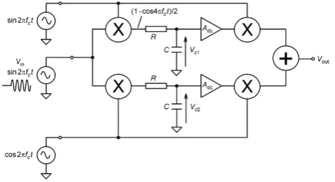
3.1. Narrowband multiplier filter for selective frequency feedback
Potential instability can be resolved by using a narrowband multiplier filter as in figure 3
(Hwang 2005, Rahal et al2009). Figure 4 shows simulations of the frequency and transient response characteristics of the circuit in figure 3 using ideal components from the ABM library in OrCAD®. The single pole response to a step is most clearly seen at Vc
1 shown in figure 4(b).
The locking frequency is fc and the low pass filters (RC = To) have poles fo= 1/To. Amplifiers
Adc can provide voltage gain at low frequencies. When Adc = 1 V V−1 at the locking frequency
the filter gain factor is 0.5. Outside the locking frequency the filter gain is attenuated. The low pass filters in figure 3 have three functions: (i) they define the narrowband bandwidth, (ii) they suppress the 2fc component generated at the outputs of the first multipliers, and (iii) they pro-vide a dominant pole to allow stability in feedback. In the steady state since one of the inputs of the second stage multipliers is dc, the outputs are independent of fo. The 2fo ripple at the output of the first multiplier is suppressed at Vc1 by a factor 2fc/fo. In the example of figure 4, fc = 100 kHz and fo = 1.6 kHz. The bandwidth in figure 4(a) is 2fo = 3.2 kHz. The resulting ripple is 7 mV p–p. Under steady state conditions at the locking frequency fc the filter transfer function has a gain of 0.5Adc and the common mode feedback analyses in section 2.2 apply.
The step response is dominated by the poles of the low pass filters whose time constants are
To = 1/fo, defined by a tradeoff between bandwidth chosen, accuracy and feedback stability.
3.2. Step response with common mode feedback
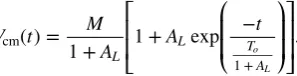
In figure 2 by adding the multiplier filter into the feedback circuit (‘Filter’ in figure 2) a stabi-lising dominant pole can be introduced at the locking frequency fc with very little phase shift. When in a feedback circuit, the step response (at the locking frequency) operates in a similar fashion to the step response of a standard operational amplifier with a dominant pole in its feedback path (Rahal et al2009). For (4) and (7) the Laplace form is
=
+ +
V s M
s
( ) 1 1
1 AsT
cm
1
L o
(10)
where M is a value depending on the feedback circuit, and AL is the loop gain of the feedback at the locking frequency.
The step response is
⎡
⎣ ⎢ ⎢
⎛
⎝ ⎜ ⎜
⎞
⎠ ⎟ ⎟ ⎤
⎦ ⎥ ⎥ =
+ + −+
V t M
A A
t ( )
1 L 1 Lexp T .
A
cm
1
o L
(11)
In (5) and (8) it has been shown that the final steady state value of Vcm is hardly altered over
a wide range of Zb. The transient term in (11) can therefore be used to determine the time taken to reach to within a certain range of the final value.
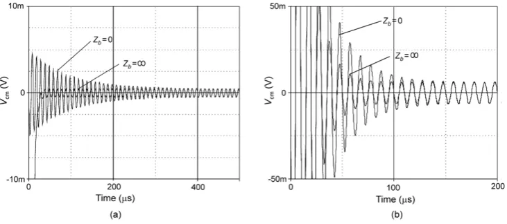
Figure 5 shows the time taken to reach within 1% of the final value as a function of the loop gain AL. For fast step response it is an advantage to have high feedback gain even though this results in the high initial values of Vcm as shown in (4) and to a lesser extent (8). From
(4) using common mode current feedback the step response is very susceptible to Zb variation compared with common mode voltage feedback (7) as shown in simulation in figure 6. Note that the linear analysis shown here breaks down when considering times below the period of the operating frequency of the narrowband filter. Feedback can also break down if there is insufficient attenuation in the low pass filter when very high loop gains are used.
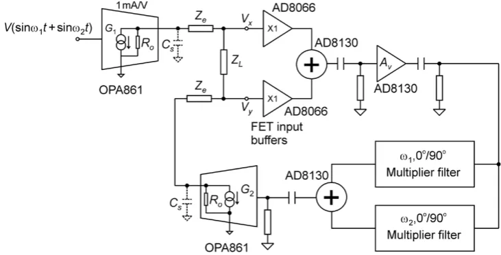
4. Experimental results using two simultaneous frequencies
Only one frequency can be processed using a multiplier filter feedback. For two or more simultaneous frequencies each frequency must have its individual multiplier filter and feed-back circuit. To demonstrate the practicality of the principle a single current drive with two simultaneous frequencies using either current (figure 2(b)) or voltage (figure 2(d)) feedback were demonstrated. Figure 7 shows the implementation of the basic common mode feedback circuit. It has two narrowband multiplier filters as shown in figure 3 (Hwang 2005). The circuit constructed uses discrete component devices. ZL = 1 kΩ and Ze = 500 Ω were used. The choice
of resistive load components was to ensure any frequency effects observed were due to the common mode structure. There was no Zb (potentially the least stable condition).
Components from Analog Devices (AD8066, AD8130, AD835) and Texas Instruments (OPA861) were installed following advice supplied in their application notes. Frequencies ranged from 50 kHz to 1 MHz. Where possible devices were ac decoupled. The dc offsets in
Figure 4. Simulations showing (a) Frequency response of the filter in figure 3; (b) Step response of filter measured at Vc1. fc = 100 kHz, fo = 1.6 kHz and Adc = 1 V V−1. The
the circuits surrounding the multipliers and low pass filter (integrator) were trimmed to within about 2 mV. This provided a suitably low baseline in spectra measurements (figures 8 and
9). Test equipment used two four-channel signal generators (TGA12104, Thurlby Thandar) and a spectrum analyser (E4411A, Agilent Technologies). The amplifier Av provided a gain of 40 V V−1 before the multiplier filter (which had an attenuation of 0.5) to ensure that errors
in the multipliers due to offsets and mismatch were minimised. The multiplier filters were adapted from those in Langlois et al2014. The input drive sinewave input was restricted so that the response could be observed over a reasonable frequency range before reaching the input limit of the multipliers. For current feedback the combination of Av before the filter and the output transconductor G2 provided a transconductance G (figure 2) of 0.022 A V−1.
The transconductors G1 and G2 had output resistances of about 50 kΩ. For voltage feedback
the transconductor G2 was replaced by an AD8066 unity gain voltage buffer. Common mode
measurements attenuated by approximately 0.2 in the connection to the spectrum analyser were monitored at V+ in figure 2 (where V+ = 2Vcm).
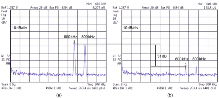
The performance when applying two sinewave signals simultaneously is shown in figures 8
and 9 for current and voltage feedback, respectively. Figures 8(a) and 9(a) show the common
Figure 5. Variation of step response with loop gain AL.
Figure 6. Simulated step response. (a) Current feedback balanced drive with I = 1 mA,
mode signals without feedback. For the current feedback the feedback transconductor input was set to 0 V. For the voltage feedback the input of the feedback voltage drive was set to 0 V. Figures 8(b) and 9(b) show the common mode signals with feedback. Common mode reduc-tion was about 62 dB for current feedback and 31 dB for voltage feedback compared with 67 dB and 32 dB from table 1. The amplitude of the input ac currents differed for current and voltage feedback measurements. The input currents, of the order of 20 μA, were adjusted to provide very approximate similar feedback common mode amplitudes.
Current mode feedback operated at lower frequencies than voltage feedback. A 3 dB drop in common mode attenuation occurred at 300 kHz. In current feedback from table 1(b) the common mode attenuation is GZo. Capacitive strays, Cs in figure 7, at higher frequencies
Figure 7. Double frequency narrowband common mode current feedback with a single current drive. The multiplier filters used the AD835 (see Langlois et al2014) and fo = 795 Hz. For voltage feedback transconductor G2 was replaced by an AD8066 configured
as a unity gain voltage buffer.
will significantly reduce Zo (= Cs || Ro) and therefore the common mode attenuation. Since
Ro = 50 kΩ the 300 kHz pole indicates Cs is about 10 pF. For voltage feedback from table 1(b) the common mode attenuation is 1/2A, and is (to a first order) independent of both Zo and ZL
and therefore can operate at frequencies mainly limited by the high frequency limit of the voltage feedback A (figure 2).
An example of the spectrum for dual frequency feedback is shown in figure 10 for volt-age feedback. To observe the spectrum of the common mode feedback a single sinewave was swept over the frequency range. The minimum frequency difference between a chosen frequency fx and its adjacent frequency fy causes a component (fx − fy) at the output of the first multiplier (figure 3) which must be attenuated by the integrator RC in the same manner as the 2fx frequency component. The integrator RC (primarily chosen to sufficiently attenuate the lowest expected 2fx component to suppress distortion (Langlois et al2014) will sufficiently attenuate the (fx − fy) component if (fx − fy) > 2fx. A designed lowest operation frequency of 10 kHz limits the minimum frequency difference to 20 kHz.
5. Discussion
Without feedback the application of a connection Zb from the body to ground can substantially
reduce the common mode voltages. However on applying feedback, analysis and simulation show that the resulting steady state common mode error voltage changes very little with Zb.
It is the step response which can be significantly affected.
The measured results show that a useful common mode reduction can be expected with dual frequency input signals. With single pole filters in the multipliers (figure 3) there is some harmonic breakthrough due to the remaining ripple on Vc1 illustrated in figure 4(b). The
addi-tion of extra frequencies each with its appropriate narrowband frequency common mode feed-back will add further harmonic components as a result of the frequency difference between two adjacent applied frequencies. This limits how close adjacent frequencies can be allowed for adequate suppression by the low pass filter RC in figure 3. The sum of input currents from multiple frequency signals cannot exceed an upper safe limit, so each signal must be reduced proportionately. The addition of unwanted signals and the reduction of drive current (and therefore differential output signals) will limit the number of frequencies possible.
Outside the locking frequencies there is little feedback. In the case of current feedback the load then remains floating, which allows capacitive coupling from external devices. For volt-age feedback outside the chosen frequencies one side of the load is held (via an electrode) at earth. In practice impedances, notably of the electrodes and the load, and strays will modify the results.
Measurements have been performed with standard discrete components. The loop gain for voltage feedback was relatively low compared with that of current feedback. There were limitations, in particular in the multipliers, figure 3, with their built in dc offsets affecting the low pass filter accuracy. The loop gain can be increased by increasing the gain of Adc in the
multiplier filters in figure 3. An integrated circuit design using a switching multiplier (Godoy and Dawson 2008) as the first stage multiplier and dc amplifiers with dc offset compensation (Enz and Temes 1996) can be used to boost the loop gain.
6. Conclusion
The problem of large common mode voltages at higher frequencies in bioimpedance appli-cations can be suppressed by adding narrowband common mode feedback. It has been suc-cessfully employed using two drives with different frequencies simultaneously. Formalised analysis of both current and voltage narrowband feedback has been presented for current input drives. The limit of the number of additional current drives will be dictated by the accumulating background noise generated by the imperfections in the narrowband feedback components. Experimental results for two simultaneous frequencies using standard available components show a reduction of 62 dB for current feedback and 31 dB for voltage feedback.
Acknowledgments
This study was supported by the UK Engineering and Physical Sciences Research Council (EPSRC) under grants EP/E029426/1 and EP/G061629/1.
Appendix A. Analysis of the balanced current feedback (figure 2(a))
The balanced current feedback in figure 2(a) has been selected as an example to demonstrate the process of analysis. The other feedback analyses follow a similar procedure. Figure 11
shows the balanced current feedback of figure 2(a). For simplicity the output impedance ZoG
of the transconductor G is assumed to be infinite and the gain of the filter to be unity. The loop gain of the feedback is then ZoGV+. It is also assumed that Zo >> Ze, ZL /2.
The current drives with their output impedances are replaced by their dual voltage drives. For analysis, the contributions of I+ and I− to V+ (=2Vcm) can be split and, using the principle
of superposition, then combined. Figure 12 shows the two circuits. Referring to figure 12(a), since Zo >> Ze the voltage Vx+ is
∑
= + +
+ + + ≈ +
+ + +
V I Z Z Z Z Z
Z Z Z Z Z I Z
Z Z Z
Z
/2 ( /2)
/2 ( /2)
( /2)
x o L o L b
o L o L b o
L o b
(A.1)
where
∑
Z≈ +Zo Zo Zb. Similarly the voltage Vy+ is∑
≈
+ +
V I Z Z Z
Z
y o o b
(A.2)
Similarly in figure 12(b)
∑
≈ − +
− − +
V I Z Z GV Z Z
Z
( )
x o o o b
(A.3)
and
∑
≈ − + +
− − +
V I Z Z GV Z Z Z
Z
( )( /2)
y o o L o b
(A.4)
By the principle of superposition
= + + +
+ + + − −
V (A.5)Vx Vy Vx Vy
and using (A.2)–(A.5) yields
Δ
= +
+ − ++
+ +
V IZ Z Z Z
Z Z Z GV Z
Z Z Z
Z Z Z
2 o( /2)L 2 o b ( )( /2) 2
o o b o
L o b
o o b
(A.6)
where 2ΔI= −I+ I−. Rearranging (A.6) gives
Δ
= =
+ +
+ ++
+
V V IZ
Z Z Z
Z Z Z
GZ Z Z Z
Z Z Z
2
( /2) 2
1 ( /2) 2
.
I o
L o b
o o b
o L o b
o o b
cm
(A.7)
References
Adler A et al 2009 GREIT: a unified approach to 2D linear EIT Physiol. Meas. 30S35–55
Anton D and Riu P J 2010 Common mode feedback analysis for EIT systems with distributed current sources J. Phys.: Conf. Ser. 224012016
Bayford R 2006 Bioimpedance tomography (electrical impedance tomography) Annu. Rev. Biomed. Eng.863–91
Bertermes-Filho P, Brown B H and Wilson A J 2000 A comparison of modified Howland circuits as current generators with current mirror type circuit Physiol. Meas. 211–6
Boone K and Holder D 1996 Current approaches to analogue instrumentation design in electrical impedance tomography Physiol. Meas. 17229–47
Casas O, Rosell J, Bragós R, Lozano A and Riu P J 1996 A parallel broadband real-time system for electrical impedance tomography Physiol. Meas.17A1–6
Enz C C and Temes G C 1996 Circuit techniques for reducing the effects of op-amp imperfections: autozeroing, correlated double sampling, and chopper stabilization Proc. IEEE841584–614
Godoy P and Dawson J L 2008 Chopper stabilization of analog multipliers, variable gain amplifiers, and mixers J. Solid-State Circuits432311–21
Hong H, Rahal M, Demosthenous A and Bayford R 2009 Comparison of a new integrated current source with the modified Howland circuit for EIT applications Physio. Meas.30999–1007
Hwang I-D 2005 Common mode feedback amplifier for biomedical measurements Proc. of the 7th IASTED Int. Conf. on Biomedical Engineering (Innsbruck, Austria, 2005) vol 458, pp 452–55
Figure 12. Contributions from the duals of the I+ (a) and I− (b) current drives to the
Hwang I-D and Park S-C 2005 Apparatus for measuring electrical impedance Patent No US 2005/0151545A1
Langlois PJ, Neshatvar N and Demosthenous A 2014 A sinusoidal current driver with an extended frequency range and multifrequency operation for bioimpedance applications IEEE Trans. Biomed. Circuits Syst. doi: 10.1109/TBCAS.2014.2332136
McEwan A, Cusick G and Holder D 2007 A review of errors in multi frequency EIT instrumentation
Phys. Meas.28S197–215
Rahal M, Demosthenous A and Bayford R 2009 An integrated common-mode feedback topology for multi-frequency bioimpedance imaging Proc. of the ESSCIRC (Athens, Greece, September 2009)
pp 416–9
Rosell J and Rui P 1992 Common-mode feedback in electrical impedance tomography Clin. Phys. Physiol. Meas. 13 A11–4