Dr. Nicola Nicolici EE2DI4 Midterm Test #2 Mar 23, 2004
Instructions: This examination paper includes 12 pages and 20 multiple-choice questions starting on page 3. You are responsible for ensuring that your copy of the paper is complete. Bring any discrepancy to the attention of your invigilator. The
answers for all the questions must be indicated by filling the corresponding circle on the optical scanning (OMR) examination sheet. This OMR examination sheet is the only page to be handed in. The instructions for completing the OMR examination sheet are provided on page 2. Read and follow these instructions with care! There is one mark for each question. Answer all questions. There is no penalty for guessing. This is a closed book exam. No reference material of any kind is permitted. No calculators of any kind are permitted. Time allowed is 50 minutes.
Multiple choice questions (numbered 1 to 20) –
indicate your answer by filling the corresponding
circle on the OMR answer sheet
Figure 1 - CMOS circuit for question 1. Figure 2 - CMOS circuit for question 2.
1. The complementary metal-oxide semiconductor (CMOS) circuit shown in Figure 1 is:
1. a 3 input XOR gate 2. a 3 input XNOR gate 3. a 2-to-1 multiplexer 4. a 4-to-1 multiplexer 5. none of the above
2. The logic function F(A,B,C) implemented by the CMOS circuit shown in Figure 2 is:
1. AB + C 2. AC + BC 3. A'B' + C'
4. A' + B'C'
3. The function implemented using 2 two-input look-up tables (LUT) as shown in Figure 3 is:
1. F(A,B,C) = Σ m(0,1,3,4)
2. F(A,B,C) = Σ m(0,1,6,7)
3. F(A,B,C) = Σ m(1,2,3,6)
4. F(A,B,C) = Σ m(1,3,4,6)
5. none of the above
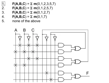
4. The programmable array logic (PAL) implementation of function F shown in Figure 4 is:
1. F(A,B,C) = Σ m(0,1,2,3,5,7)
2. F(A,B,C) = Σ m(0,1,2,5,7)
3. F(A,B,C) = Σ m(0,1,2,7)
4. F(A,B,C) = Σ m(0,1,7)
5. none of the above
[image:4.612.72.452.118.383.2]
Figure 3 – Circuit for question 3.
[image:4.612.66.440.413.699.2]5. 64 bytes are equal to:
1. 1 Kbits 2. 2 Kbits 3. 3 Kbits 4. 4 Kbits
5. none of the above
6. Consider a read-only memory (ROM) that performs binary to 4-digit BCD conversion as follows. The binary number is applied on the input address lines and the equivalent 4-digit BCD number is read on the output data lines. The capacity of the smallest ROM, in terms of the total number of bits that can be stored in it, which can be used for the conversion is:
1. 16 Kbits 2. 16 Kbytes 3. 32 Kbits 4. 32 Kbytes
5. none of the above
7. LIBRARY IEEE;
USE IEEE.std_logic_1164.all;
ENTITY question7 IS
PORT (A, B, C: IN STD_LOGIC; F: OUT STD_LOGIC); END question7;
ARCHITECTURE Behavior OF question7 IS SIGNAL W: STD_LOGIC_VECTOR(0 TO 2); BEGIN
W(2) <= A; W(1) <= B; W(0) <= C; WITH W SELECT
F <= '0' WHEN "001", '0' WHEN "110", '1' WHEN OTHERS; END Behavior;
The above VHDL code describes:
1. F(A,B,C) = A'BC + AB'C'
2. F(A,B,C) = (A'+B+C) (A+B'+C') 3. F(A,B,C) = A'B'C + ABC'
4. F(A,B,C) = (A'+B'+C)(A+B+C') 5. none of the above
Tip for question 6:Note, the range of the unsigned decimal numbers that are converted from their binary representation to their 4-digit BCD
representation is 0 to 9999. First you should determine the values for the
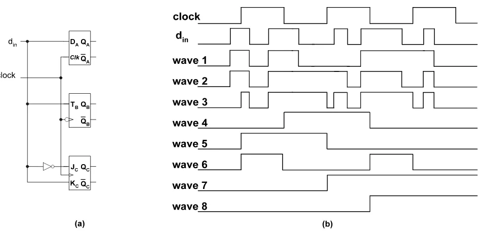
Figure 5 - Sequential (or storage) elements and signal waveforms for questions 8, 9 and 10. Note, the initial value of all the storage elements is zero and they are assumed to be ideal, i.e., the propagation delays and setup/hold times are considered to be zero.
8. Given the clock and din waveforms in Figure 5(b) the waveform for QA from Figure 5(a) is:
1. wave 1 from Figure 5(b) 2. wave 2 from Figure 5(b) 3. wave 3 from Figure 5(b) 4. wave 4 from Figure 5(b) 5. wave 5 from Figure 5(b)
9. Given the clock and din waveforms in Figure 5(b) the waveform for QB from Figure 5(a) is:
1. wave 4 from Figure 5(b) 2. wave 5 from Figure 5(b) 3. wave 6 from Figure 5(b) 4. wave 7 from Figure 5(b) 5. wave 8 from Figure 5(b)
10. Given the clock and din waveforms in Figure 5(b) the waveform for QC from Figure 5(a) is:
Figure 6 - Circuit for question 11.
11. In Figure 6, if enable=1 and the current (or present) state is Q3Q2Q1Q0=0101, then the next state will be:
1. 1111 2. 1010 3. 1100 4. 0011 5. 0000
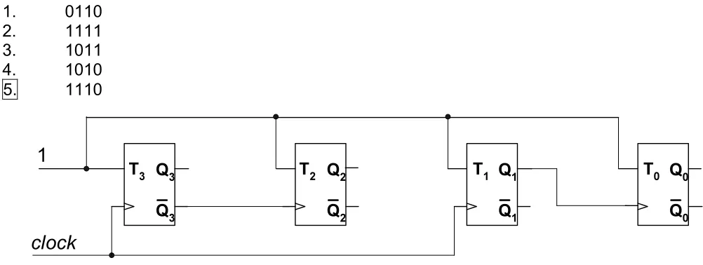
12. In Figure 7, if the current state is Q3Q2Q1Q0=0101, then after the next positive edge of the
clock signal the new state will be: 1. 0110
2. 1111 3. 1011 4. 1010 5. 1110
Figure 7- Circuit for question 12.
Note for question 12: Because NOT all the flip-flops’ clock inputs share the same
[image:7.612.62.563.450.639.2]Figure 8 - Circuit for question 13 (it is assumed that after power up the state is 000).
13. The periodic sequence Q2Q1Q0 generated by the circuit shown in Figure 8 is:
1. 000,110,001,111 2. 000,101,010,111 3. 000,100,001,111 4. 000,110,011,111 5. none of the above
Figure 9 - Circuits for question 14 (it is assumed that after power up the state is 010).
14. Using a 3-bit synchronous up counter with parallel load capability (Q2 and D2 are the most significant bits) we can generate a counting sequence 2, 3, 4, 5, 6 using the circuit shown in:
1. Figure 9(a) 2. Figure 9(b) 3. Figure 9(c) 4. Figure 9(d)
5. none of the above
15. Which of the circuits shown in Figure 10 (see next page) are equivalent?
Figure 10 - Circuits for question 15.
Figure 12 - Circuit implementations for questions 16, 17 and 18.
16. Consider the state transition table of a sequential circuit shown in Figure 11(a) (see previous page). If in our technology library we have only one JK flip-flop, one D flip-flop and one T flip-flop, then a generic implementation is shown Figure 11(b) (see previous page). Based on the state transition table and circuit topology shown in Figure 11, the logic function, which drives the input DA of the leftmost flip-flop from Figure 11(b) is shown in:
1. Figure 12(a) 2. Figure 12(b) 3. Figure 12(c) 4. Figure 12(d) 5. Figure 12(e)
17. Consider the state transition table of a sequential circuit shown in Figure 11(a) (see previous page). If in our technology library we have only one JK flip-flop, one D flip-flop and one T flip-flop, then a generic implementation is shown Figure 11(b) (see previous page). Based on the state transition table and circuit topology shown in Figure 11, the logic function, which drives the input TB of the center flip-flop from Figure 11(b) is shown in:
1. Figure 12(a) 2. Figure 12(b) 3. Figure 12(c) 4. Figure 12(d) 5. Figure 12(e)
18. Consider the state transition table of a sequential circuit shown in Figure 11(a) (see previous page). If in our technology library we have only one JK flip-flop, one D flip-flop and one T flip-flop, then a generic implementation is shown Figure 11(b) (see previous page). Based on the state transition table and circuit topology shown in Figure 11, the logic function, which drives the input KC of the rightmost flip-flop from Figure 11(b) is shown in:
Figure 13 - Circuit for question 19.
19. Consider the sequential circuit shown in Figure 13. Consider the following state
assignment: A stands for Q=0, B stands for Q=1. The state transition diagram for the circuit from Figure 13 is shown in:
1. Figure 14(a) 2. Figure 14(b) 3. Figure 14(c) 4. Figure 14(d) 5. none of the above
[image:11.612.59.552.364.633.2]Figure 15 - Circuit for question 20.
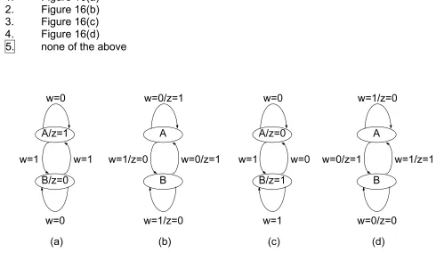
20. Consider the sequential circuit shown in Figure 15. Consider the following state
assignment: A stands for Q=0, B stands for Q=1. The state transition diagram for the circuit from Figure 15 is shown in:
1. Figure 16(a) 2. Figure 16(b) 3. Figure 16(c) 4. Figure 16(d) 5. none of the above
Figure 16 - State transition diagrams for question 20.
[image:12.612.62.552.330.623.2]