Http://www.ijetmr.com©International Journal of Engineering Technologies and Management Research [130]
HIGH SPEED ADDER USING GDI TECHNIQUE
Merrin Mary Solomon 1, Neeraj Gupta 2, Rashmi Gupta 2
1
M.Tech Student, Amity School of Engineering & Technology Amity University Haryana, Gurugram, India
2
Assistant Professor, Amity School of Engineering & Technology Amity University Haryana, Gurugram, India
Abstract:
Full adder is an important component for designing a processor. As the complexity of the circuit increases, the speed of operation becomes a major concern. Nowadays there are various architectures that exist for full adders. In this paper we will discuss about designing a low power and high speed full adder using Gate Diffusion Input technique. GDI is one of the present day methods through which one can design logical circuits. This technique will reduce power consumption, propagation delay, and area of digital circuits as well as maintain low complexity of logic design. The performance of the proposed design is compared with the contemporary full adder designs.
Keywords: Gate Diffusion Input; Full Adder; Power Dissipation; CMOS Logic; Delay.
Cite This Article: Merrin Mary Solomon, Neeraj Gupta, and Rashmi Gupta. (2018). “HIGH SPEED ADDER USING GDI TECHNIQUE.” International Journal of Engineering
Technologies and Management Research, 5(2:SE), 130-136. 10.29121/ijetmr.v5.i2.2018.634.
1. Introduction
In many of the VLSI applications such as Digital Image Processing (DSP), microprocessors and many more, we see the substantial use of adders. The arithmetic operations such as addition, subtraction, division, multiplication are all performed with the help of adders. Hence adders play an important role in the performance of the system and so designers are vigorously working in improving the performance of adders to enhance the overall performance. The use of portable devices such as laptops, mobile phones are increasing on an exponential rate. The power available for these portable devices is limited. Researchers have been extensively working on designing low power systems as it has been a major design parameter now days. Researchers have come up with different full adder designs that can bring about systems with high performance and low power utilization.
Http://www.ijetmr.com©International Journal of Engineering Technologies and Management Research [131] 2. Full Adders
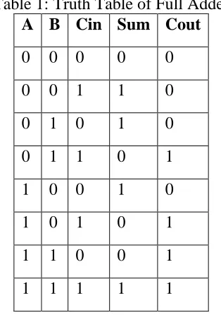
Full adder is a combinational circuit which has 3 inputs bits .It performs addition operation. Basically it has 3 inputs and 2 outputs. The Fig 1 shows the logical structure of full adder. Here we can see the 3 inputs are A, B and Cin and the outputs are expressed using Sum(S) and carry (Cout).Table 1 gives the truth table of a 1-bit full adder. The Boolean equation of the full adder is given by,
Sum= ((A⊕B) ⊕Cin) ………(1)
Cout=A.B+B.C+A.B ………(2)
Figure 1: Full adder circuit
A full adder can be designed using two half adders. A full adder can be used to construct different counters such as ripple carry counter to add n-bit number. Full adders are generally connected in a cascade manner to build various logical circuits. [4]
Table 1: Truth Table of Full Adder
A B Cin Sum Cout
0 0 0 0 0
0 0 1 1 0
0 1 0 1 0
0 1 1 0 1
1 0 0 1 0
1 0 1 0 1
1 1 0 0 1
1 1 1 1 1
3. Existing Full Adder Topologies
3.1.Conventional CMOS Full Adder
Http://www.ijetmr.com©International Journal of Engineering Technologies and Management Research [132] Remarkable advantage of this full adder topology is the ability to produce full swing voltages. Fig 2 shows the structure of CMOS full adder. The drawbacks of this circuit are that it produces unwanted delays because sum realizes on Cout signal, it dissipates more power and since the number of transistors is high, it occupies larger area.[2]
Figure 2: Conventional CMOS Full adder
3.2.CPL Full Adder
Complementary Pass transistor logic (CPL) based full adder circuit. It comprises of complimentary inputs/outputs, a NMOS pass transistor circuit and CMOS output inverters. In addition to this, PMOS keeper circuit is used to reduce static power consumption and also for swing restoration. The system basically consists of two stage pass transistor network. In the first stage, the network is designed by applying true inputs to pass transistor logic and second stage is designed by applying complementary inputs to pass transistor logic. The drawback of CPL full adder is that the number of transistors used is more. Here 32 transistors are used and hence it occupies more area. Another drawback is that in the NMOS network swing-reduction has to be restored. Fig 3 shows the structure of CPL full adder.
Figure 3: CPL full adder 3.3.Hybrid Full Adder
Http://www.ijetmr.com©International Journal of Engineering Technologies and Management Research [133] of this circuit is comparatively high when comparing to the other counterparts and this is because the critical path consists of only two transistors.
Figure 4: Hybrid Full adder
3.4.ULP Full Adder
The ULP full adder uses CMOS logic as well as pass-transistor logic for designing the full adder. The main feature of this circuit is the addition of a unique voltage restorer, ULP diode. It will eliminate the need for speed compensation at the output. Fig 5 shows the design of ULP full adder. This circuit design is resilient against voltage scaling and also it is difficult to implement transistor sizing. Since the design comprises of two different logics, it is non-symmetrical and irregular in design. [1], [3]
Figure 5: ULP Full adder
4. Proposed Design
Http://www.ijetmr.com©International Journal of Engineering Technologies and Management Research [134] GDI technique is much efficient. Even though the technique has many advantages, there are few drawbacks which can be rectified. A GDI cell consists of 3 inputs. One input G which is the gate input for PMOS and NMOS, P which is the input to source/drain of PMOS and N which is the input to source/drain of NMOS.
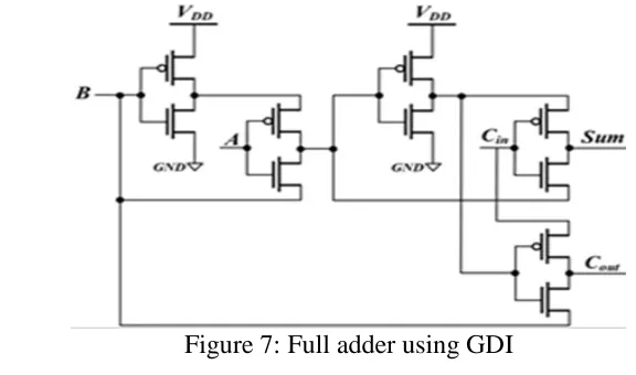
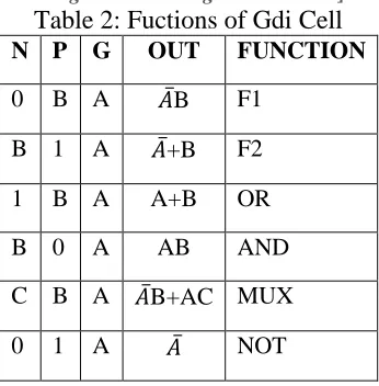
The major benefit of using GDI technique is that a large number of functions can be implemented using this technique. We can see from the table 2 that GDI can be used for implementing various designs such as MUX, AND, OR etc. The most complex design among these is the designing of MUX, which can be done using 2 transistors. Whereas using other conventional techniques it requires 8-10 transistors for designing a MUX. The main drawback of GDI technique is that of swing degradation. This is due to threshold loss and to eliminate this we have to use silicon on insulator or twin-well process to realize, which is very expensive. Designing a full adder the major building block is XOR gate using GDI technique. The design is shown in the Fig 7.
Figure 6: GDI cell
The major benefit of using GDI technique is that a large number of functions can be implemented using this technique. We can see from the table 2 that GDI can be used for implementing various designs such as MUX, AND, OR etc. The most complex design among these is the designing of MUX, which can be done using 2 transistors. Whereas using other conventional techniques it requires 8-10 transistors for designing a MUX. The main drawback of GDI technique is that of swing degradation. This is due to threshold loss and to eliminate this we have to use silicon on insulator or twin-well process to realize, which is very expensive. Designing a full adder the major building block is XOR gate using GDI technique. The design is shown in the Fig 7.
Http://www.ijetmr.com©International Journal of Engineering Technologies and Management Research [135] Table 2: Fuctions of Gdi Cell
N P G OUT FUNCTION
0 B A ̅B F1
B 1 A ̅+B F2
1 B A A+B OR
B 0 A AB AND
C B A ̅B+AC MUX
0 1 A ̅ NOT
In here 5 PMOS and 5 NMOS transistors are used. In total only 10 transistors are used to design the full adder. A, B, Cin are the input and Cout and sum are the output produced.
5. Comparison and Analysis
Table 3: Performance Analyses
No. Of Transistors Delay(ps) Power(µw) PDP
CMOS 28 98.46 3.903 0.384
CPL 32 110 3.91 0.0431
ULP 20 22.66 2.73 0.061
Hybrid 20 6.706 4.103 0.027
GDI 10 31.48 2.449 0.077
Here we have discussed about 5 full adders including the proposed system. We are comparing these adders on the basis of three criterions power, delay and the number of transistors used. The resultant power and delay value can be used to find the power delay product (PDP). From the table 3, it is clear that the better full adder is the proposed full adder which is designed using GDI technique. The number of transistors used in GDI technique is minimum compared to other full adders used here. The power dissipation of full adder designed using GDI technique is the least when compared to the other discussed full adders.
6. Conclusion
Http://www.ijetmr.com©International Journal of Engineering Technologies and Management Research [136] were obtained as an outcome of simulation, the readings are precise. This design will have an improved speed and also the efficiency of the system is more compared to all the conventional techniques. Further modifications can be made in the design by adding a few more transistors.
References
[1] K. Navi, M.H. Moaiyeri, R. FaghihMirzaee, O. Hashemipour, B. MazloomNezhad, Two new low-power full adders based on majority-not gates, Microelectronics Journal (Elsevier), 40, 126– 130.
[2] M.H. Moaiyeri, R. FaghihMirzaee, K. Navi, T. Nikoubin, O. Kavehei, Novel direct designs for 3-input XOR function for low power and high-speed applications, International Journal of Electronics (Taylor and Francis) 97 (6) (2010) 647–662.
[3] K. Navi, M. Maeen, V. Foroutan, S. Timarchi, O. Kavehei, A novel low power full-adder cell for low voltage, Integration the VLSI Journal (Elsevier) 42 (4) (2009) 457–467.
[4] M. Alioto, G. Palumbo, Analysis and comparison of the full adder block, IEEE Transactions on VLSI 10 (6) (2002) 806–823.
[5] C.H. Chang, J. Gu, M. Zhang, A review of 0.18 um full-adder performances for tree structure arithmetic circuits, IEEE Transactions on Very Large Scale Integration(VLSI)Systems 13 (6) (2005).
[6] A.M. Shams, T.K. Darwish, M.A. Bayoumi, Performance analysis of low-power 1-bit CMOS full adder cells, IEEE Transactions on Very Large Scale Integration (VLSI) Systems 10 (1) (2002) 20–29.
[7] Arkadiy Morgenshtein, A. Fish, Israel A. Wagner, Gate-diffusion input (GDI): a power-efficient method for digital combinatorial circuits, IEEE Transactions on VLSI Systems (2002) 566–581. [8] R. Zimmermann, W. Fichtner, Low-power logic styles: CMOS versus pass- transistor logic, IEEE
Journal of Solid-State Circuits 32 (1997) 1079–1090.
*Corresponding author.