Effect of Through Cage on Active Screen Plasma Nitriding Properties
Akio Nishimoto, Atsushi Tokuda
*and Katsuya Akamatsu
Department of Chemistry and Materials Engineering, Faculty of Chemistry, Materials and Bioengineering, Kansai University, Suita 564-8680, Japan
Low carbon steel S15CK was nitrided by active screen plasma nitriding (ASPN) using various stainless steel cages to investigate the effect of the cage on the nitriding properties. Three types of austenitic stainless steel cages, such as pipe, foil, and wire mesh, were used. The sample was treated for 18 ks at 773 K under 630 Pa in 50% N2+ 50% H2gases. The nitrided samples were characterized by surface roughness tests, optical microscopy, scanning electron microscopy, X-ray diffraction, and microhardness testing. In all samples nitrided by the ASPN process, the ‘edging effect’ was completely eliminated whereas hardness and thickness of the surface layer were comparable with those obtained from the DC plasma nitriding. Moreover, a comparison of the screens used in the ASPN process revealed that the screen hole size had a slight influence on surface properties such as microstructure and hardness. [doi:10.2320/matertrans.MRA2008431]
(Received November 25, 2008; Accepted February 6, 2009; Published April 2, 2009)
Keywords: active screen plasma nitriding, DC plasma nitriding, through cage, edging effect, steel, surface engineering
1. Introduction
Nitriding process is widely used for improving the tribological properties and wear resistance of steels and titanium alloys. Glow discharge plasma nitriding process is more advantageous compared with the conventional nitrid-ing processes such as gas nitridnitrid-ing and salt bath nitridnitrid-ing, e.g., no pollution, high nitrogen potential, short treatment time, clean environment, and little energy consumption.1–6) The components treated are subjected to a high cathodic potential to produce the plasma directly on its surface. ‘Edging effect’ occurred due to distortions of the electric field around the corners and edges of the components, even though the components were heated effectively. This results in non-uniformity of properties of the surface layer, such as hardness and thickness.7)
Recently there has been considerable interest in active screen plasma nitriding (ASPN), through cage plasma nitriding (TCPN), and cathodic cage plasma nitriding (CCPN).8–25) In this process, the edging effect was com-pletely eliminated, because the plasma was produced on the cage and not directly onto the samples.10)This process can be used to treat ceramics and polymer, which are non-conductive materials.15,17,25) However, little information has been reported regarding the effect of the thickness and hole-size of the cage on the nitriding properties.
In this study, ASPN using various cages has been performed on a low carbon steel sample to investigate the effect of the cage on the nitriding properties.
2. Experimental Details
2.1 Experimental apparatus
Plasma nitriding experiments were performed using a DC plasma nitriding unit (Fuji Electronic Industry Co., Ltd. Japan, FECH 1N). Three through cage arrangements, as schematically shown in Fig. 1, were used during the nitriding
treatment. In Fig. 1, the cage, an austenitic stainless steel, with 42 mm diameter and 25 mm height was mounted on a stage and connected to a cathodic potential. Alumina (Al2O3)
ceramics, 3 mm in thickness, were placed on the cathodic stage. The sample was located in a floating potential, isolated from the cathodic cage screen and the anode, and placed on an Al2O3ceramics insulator so that the distance between the
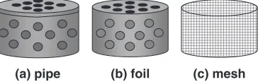
sample and the cage was 10 mm. As shown in Fig. 2(a), a cylinder was cut from a stainless steel pipe of 42 mm outer diameter and 3 mm thickness, which had uniformly dis-tributed round holes of 5 mm diameter. In Fig. 2(b), a cage was made from a stainless steel foil of 0.5 mm thickness, which had uniformly distributed round holes of 5 mm diameter. In Fig. 2(c), a cage was made from a stainless steel wire mesh. The mesh size was1010mesh. The cages were well degreased ultrasonically in acetone. On the other hand, in conventional DC plasma nitriding (DCPN), the samples to be treated were in a cathodic potential and the furnace wall was in an anodic potential.
10 mm
10 mm
Cage
Insulator Sample
Fig. 1 Schematic illustration of a through cage setup.
(c) mesh (b) foil
(a) pipe
Fig. 2 Schematic illustration of through cages during active screen plasma nitriding: (a) pipe, (b) foil, and (c) wire mesh.
*Graduate Student, Kansai University. Present address: NTN Corporation,
[image:1.595.347.505.314.409.2] [image:1.595.337.519.454.512.2]2.2 Materials
The sample material used in this study was a low carbon steel S15CK (nominal composition (mass%): 0.12–0.18% C, 0.15–0.35% Si, 0.30–0.60% Mn,<0:030% P, <0:030% S, balance Fe). The sample disc was 16 mm in diameter and 10 mm in thickness. The sample surface was mechanically ground from 150 to 1500-grit SiC, finely polished with 0.05mmalumina suspension, further degreased ultrasonically in acetone, and dried in air before placement into a nitriding furnace.
2.3 Processing
All treatments of ASPN and DCPN were carried out using the same parameters as shown in Table 1. After placing the sample on the sample stage, the chamber was evacuated at 3Pa. Nitrogen and hydrogen gases were then introduced into the chamber and a DC bias voltage was supplied. The sample temperature was measured directly using a chromel-almel (type-K) thermocouple. After nitriding, the DC supply was switched off and the sample was cooled to room temperature in the furnace.
2.4 Characterization
After nitriding, the cross sections of each sample were cut using a low-speed saw, polished, and chemically etched in 3% Nital solution. The nitrided microstructure was examined using an optical microscope (OM). The morphologies of the ASPN- and DCPN-treated surfaces were observed with a scanning electron microscope (SEM). X-ray diffraction (XRD) was used to determine the phase structures at the nitrided surface. A whole area of the top surface of nitrided
samples was analyzed by XRD. The surface roughness was determined using Surftest-402 and Surftest Analyzer 178 Series manufactured by Mitutoyo Co., Ltd. A central part of the nitrided surface was analyzed in the surface roughness test. In addition, a test to determine the hardness of the surface and cross-sections of the nitrided sample was conducted using a Vickers microhardness tester under 0.5 N load.
3. Results and Discussion
S15CK low carbon steel samples were plasma nitrided for 3.6–18 ks at 773 K under 630 Pa in 50% N2 + 50% H2gases
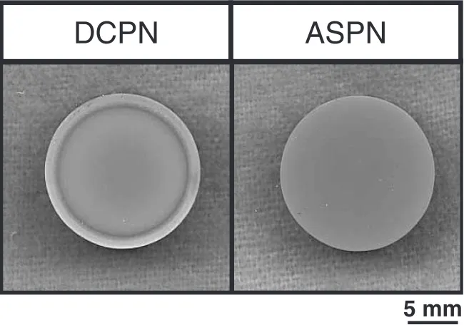
using ASPN and DCPN processes. Pipe, foil, and wire mesh of stainless steels were used as cages in the ASPN process. After treatment, the appearance of the samples was visually examined as shown in Fig. 3. In the sample treated by the DCPN process, the ‘edging effect’, which showed a ring with a different color from the central area of the sample surface, was observed. In contrast, the edging effect was not observed in all the samples treated by the ASPN process. It was believed that a glow discharge did not occur on the sample surface because of the isolation of the sample by placing the Al2O3 ceramics between the sample and the
stage. Furthermore, in the ASPN process, samples were heated to reach the treatment temperature by the heat radiated from the cage, which promoted higher homogeneity of the temperature in the treated samples.11)
XRD results of the samples treated for 18 ks by the ASPN and DCPN processes are shown in Fig. 4. "-Fe2-3N, 0
-Fe4N, and -ferrite were identified in each sample.
Com-pared with the DCPN-treated sample, a strong diffraction peak of the "-Fe2-3N phase was detected for the
ASPN-treated samples, whereas a weak diffraction peak of the
0-Fe4N phase was detected.9,10,20) It is well known that
[image:2.595.136.461.73.301.2]sputtering and decarburizing occur during the DCPN process due to the direct interaction of the plasma species with the Table 1 Processing parameters for plasma nitriding.
Temperature Time Pressure H2:N2 Voltage Current
773 K 3.6 and 18 ks 630 Pa 50 : 50 250 V 0.4 A
DCPN
ASPN
5 mm
[image:2.595.43.292.364.389.2]sample surface.26)According to the Fe-N-C phase diagram, the "-Fe2-3N phase has a wider nitrogen and carbon
solubility range compared with the 0-Fe
4N phase.27) In
the ASPN process, the sputtering does not occur on the sample surface, but rather occurs on the cage, eliminating the surface decarburizing that contributes to the largest formation of"-Fe2-3N phase.20)
Moreover, in each sample treated by the ASPN process, the diffraction in the 0-Fe4N phase increased with
in-creasing treatment time, whereas that of the"-Fe2-3N phase
decreased. This may have occurred because of the decom-position of FeN due to long treatment time, which resulted in more0-Fe
4N formation on the sample surface.
Figure 5 shows the result of surface roughness measure-ments of the ASPN- and DCPN-treated samples. In each sample, the surface roughness tended to increase with the nitriding time. It was believed that a compound layer resulting from the decomposition of FeN on the sample
surface grew with increasing nitriding time. Moreover, the surface roughness of the sample treated by the ASPN process using various cages tended to be suppressed compared with that treated by the DCPN process. This result indicates that iron nitride was deposited and grown homogeneously, resulting from the lack of ionbombardment on the sample surface during the ASPN process.
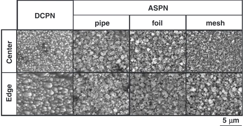
Figure 6 shows SEM micrographs of the sample surfaces treated by the ASPN and DCPN processes. The shape of the surface morphology treated by the DCPN process was different at the center and edges. In contrast, polygonal particles with a normal distribution were observed at the center and edges of the ASPN-treated sample surfaces. This may be because FeN particles in the plasma, which were formed on the cage, deposited on the sample surface for the ASPN process, whereas the glow discharge accelerated to the edge of the sample for the DCPN process. Particles on the sample surface treated for 18 ks were coarser than those treated for 3.6 ks. This result indicates that the FeN deposition increased with increasing treatment time, and these deposited particles grew. Comparison of the ASPN-treated samples revealed that the particles on the sample surface treated with the wire mesh screen were slightly finer than those treated with other screens.
20° 40° 60° 80°
Intensity (arbitrary unit)
Diffraction angle, 2θ
DCPN
ASPN (pipe)
ASPN (foil)
ASPN (mesh)
γ α-Fe
Fig. 4 XRD results of the samples treated for 18 ks at 773 K by the ASPN and DCPN processes.
Roughness,
Ra
/
µµ
m
0 0.02 0.04 0.06 0.08
0.12
3.6 ks
18 ks
DCPN ASPN
(foil)
ASPN (mesh)
0.10
(pipe) ASPN
Fig. 5 Surface roughness profile of the ASPN and DCPN treated samples.
DCPN
ASPN
mesh
Center
pipe
5
µ
m
foil
Edg
e
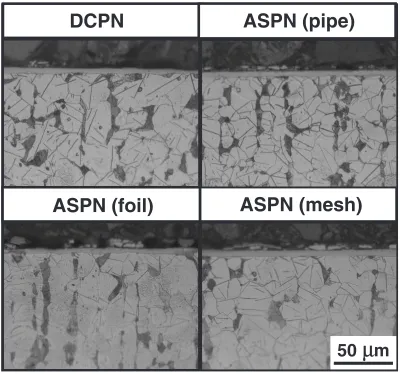
[image:3.595.55.285.71.265.2] [image:3.595.314.540.78.209.2] [image:3.595.98.496.559.766.2]The microstructures of the cross-section of the samples treated for 18 ks by the ASPN and DCPN processes are shown in Fig. 7. The compound layer at the surface followed by the diffusion layer were observed in all the samples. Needle-like precipitates were observed in the diffusion layer. The compound layer and the diffusion layer tended to increase with increasing nitriding temperature. This may be because the compound layer grew with decomposing FeN, resulting in nitrogen diffusion from the compound layer into the substrate core. A comparison of the ASPN- and the DCPN-treated samples revealed that the thickness of the compound layer was similar. On the other hand, comparison of the ASPN-treated samples revealed that the thickness of the surface layer treated with the mesh screen was slightly greater than those treated with other screens.
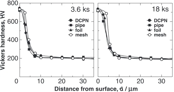
Figure 8 shows the cross-sectional hardness distribution of the samples treated by the ASPN and DCPN processes under each condition. In each sample treated by the ASPN and DCPN processes under all nitriding conditions, the surface hardness considerably increased (700HV) and the hardness decreased toward the core of the substrate. Moreover, the hardness in the diffusion layer was higher than that of the S15CK substrate. This increase of the hardness can be explained by the fact that the diffusion layer was precip-itation-hardened because of the precipitation of0-Fe
4N, as
shown in Fig. 7. Comparison of the ASPN-treated samples revealed that the thickness of the hardened layer treated with the mesh screen was slightly greater than those treated with other screens.
From the results of the cross-sectional microstructure and hardness distribution, as shown in Figs. 7 and 8, the thickness of the hard compound layer and diffusion layer increased with increasing treatment time. This indicates that the thickness of the hard compound layer increased because of long treatment time, and the thickness of the diffusion layer increased because of the diffusion of the nitrogen from the sample surface into the substrate core. A comparison of the ASPN-treated samples revealed that the thickness of the compound layer treated with the wire mesh screen was slightly greater than those treated with other screens.
Based on the above-mentioned results, the edging effect was not observed in each sample treated by the ASPN process using various cages, indicating that three types of cages used in this investigation were beneficial for the ASPN process. A comparison of the samples treated by the ASPN process revealed that surface properties such as phase, microstructure, and hardness were almost similar, although the sample treated with the mesh screen showed a surface layer with slightly finer particles and slightly greater thick-ness than those treated with other screens. These results
DCPN
ASPN (pipe)
ASPN (foil)
ASPN (mesh)
m
50
µ
[image:4.595.98.498.71.445.2]indicate that the cage hole size has a slight effect on the nitriding properties. Detailed studies need to be conducted to clarify this.
4. Conclusions
Low carbon steel has been treated by the ASPN process using three types of stainless steel cages of a pipe, foil, and wire mesh to investigate the effect of the cage on the plasma nitriding properties. In all samples treated by the ASPN process, the edging effect was completely eliminated, and a compound layer on the surface followed by a diffusion layer were observed. In addition, ASPN showed similar character-istics, such as phase, hardness, and thickness of the surface layer, compared with DCPN. Moreover, a comparison of the samples treated by the ASPN process using various cages revealed that the surface layer of the sample treated with the wire mesh screen was slightly finer and thicker compared with the samples treated with other screens. This result indicates that the cage hole size has a slight influence on the ASPN properties.
REFERENCES
1) Y. Sun and T. Bell: Mater. Sci. Eng. A140(1991) 419–434. 2) M. Samandi, B. A. Shedden, D. I. Smith, G. A. Collins, R. Hutchings
and J. Tendys: Surf. Coat. Technol.59(1993) 261–266.
3) M. A. J. Somers and E. J. Mittemeijer: Metall. Mater. Trans. A26A (1995) 57–74.
4) B. Zhao, J. Sun, J. S. Wu and Z. X. Yuan: Scr. Mater. 46(2002) 581–586.
5) K. Funatani: Met. Sci. Heat Treat.46(2004) 277–280.
6) H. Berns, R. L. Juse, J. W. Bouwman and B. Edenhofer: Heat Treat.
Met.27(2000) 39–45.
7) C. Alves Jr., E. F. da Silva and A. E. Martinelli: Surf. Coat. Technol. 139(2001) 1–5.
8) J. Georges: Heat Treat. Met.28(2001) 33–37. 9) D. Cleugh: Surf. Eng.18(2002) 133–139.
10) C. X. Li, T. Bell and H. Dong: Surf. Eng.18(2002) 174–181. 11) C. X. Li, J. Georges and X. Y. Li: Surf. Eng.18(2002) 453–458. 12) C. X. Li and T. Bell: Heat Treat. Met.30(2003) 1–7.
13) C. X. Li and T. Bell: Corros. Sci.46(2004) 1527–1547. 14) C. X. Li and T. Bell: Wear256(2004) 1144–1152.
15) C. X. Li and T. Bell: J. Mater. Process. Technol.168(2005) 219–224. 16) Sh. Ahangarani, F. Mahboubi and A. R. Sabour: Vacuum80(2006)
1032–1037.
17) C. X. Li, H. Dong and T. Bell: J. Mater. Sci.41(2006) 6116–6118. 18) P. Hubbard, S. J. Dowey, E. D. Doyle and D. G. McCulloch: Surf. Eng.
22(2006) 243–247.
19) C. Zhao, C. X. Li, H. Dong and T. Bell: Surf. Coat. Technol.201(2006) 2320–2325.
20) C. Alves Jr., F. O. de Araujo, K. J. B. Ribeiro, J. A. P. da Costa, R. R. M. Sousa and R. S. de Sousa: Surf. Coat. Technol.201(2006) 2450–2454.
21) R. R. M. de Sousa, F. O. de Araujo, K. J. B. Ribeiro, M. W. D. Mendes, J. A. P. da Costa and C. Alves Jr.: Mater. Sci. Eng. A465(2007) 223–227.
22) Sh. Ahangarani, A. R. Sabour and F. Mahboubi: Appl. Surf. Sci.254 (2007) 1427–1435.
23) K. J. B. Ribeiro, R. R. M. de Sousa, F. O. de Araujo, R. A. de Brito, J. C. P. Barbosa and C. Alves Jr.: Mater. Sci. Eng. A 479(2008) 142–147.
24) R. R. M. de Sousa, F. O. de Araujo, J. C. P. Barbosa, K. J. B. Ribeiro, J. A. P. da Costa and C. Alves Jr.: Mater. Sci. Eng. A487(2008) 124–127.
25) A. P. Kauling, G. V. Soares, C. A. Figueroa, R. V. B. de Oliveira, I. J. R. Baumvol, C. Giacomelli and L. Miotti: Mater. Sci. Eng. C29 (2009) 363–366.
26) C. Ruset, S. Ciuca and E. Grigore: Surf. Coat. Technol.174–175(2003) 1201–1205.
27) J. Slycke, L. Sproge and J. Agren: Scand. J. Metall.17(1988) 122–126.
0
10
20
30
0
10
20
30
200
400
600
800
Vickers hardness,
HV
Distance from surface,
d
/
µ
m
3.6 ks
18 ks
DCPN pipe foil mesh
DCPN pipe foil mesh
[image:5.595.129.471.75.257.2]