Dielectric waveguide vertically coupled to all-silicon photodiodes operating at
telecommunication wavelengths
Kapil Debnath, Frederic Y. Gardes, Andrew P. Knights, Graham T. Reed, Thomas F. Krauss, and Liam O'Faolain
Citation: Applied Physics Letters 102, 171106 (2013); doi: 10.1063/1.4803541
View online: http://dx.doi.org/10.1063/1.4803541
View Table of Contents: http://scitation.aip.org/content/aip/journal/apl/102/17?ver=pdfcov
Dielectric waveguide vertically coupled to all-silicon photodiodes
operating at telecommunication wavelengths
Kapil Debnath,1,a)Frederic Y. Gardes,2Andrew P. Knights,3Graham T. Reed,2 Thomas F. Krauss,4and Liam O’Faolain1
1
SUPA, School of Physics & Astronomy, University of St Andrews, North Haugh, St Andrews KY16 9SS, United Kingdom
2
Optoelectronics Research Centre, University of Southampton, Southampton SO17 1BJ, United Kingdom 3
Department of Engineering Physics, McMaster University, Hamilton, Ontario L8S 4L7, Canada 4
Department of Physics, University of York, York YO10 5DD, United Kingdom
(Received 29 January 2013; accepted 17 April 2013; published online 30 April 2013)
We present a method for detecting light in the 1550 nm wavelength window based on a silicon nitride waveguide that is vertically coupled to a silicon photonic crystal cavity. The absorption in silicon arises from deep-levels created by ion implantation, thereby providing excellent CMOS compatibility. We demonstrate a responsivity of 0.108 A/W at10 V reverse bias with a dark current of 9.4 nA. Our work demonstrates one of the smallest wavelength selective photodectors realised to date. By cascading such detectors we also demonstrate a two-channel demultiplexer.
VC 2013 AIP Publishing LLC[http://dx.doi.org/10.1063/1.4803541]
Today’s electronics industry is confronted with a serious bottleneck due to the prohibitive energy consumption and limited transmission bandwidth of copper interconnects. Energy efficient wavelength division multiplexing (WDM) offers a solution to this problem, especially with silicon-based components that can be integrated monolithically with CMOS circuits and be mass-produced at low cost.1
Significant progress in the development of all-silicon based modulators and passive optical components has al-ready been made, yet photodetection typically requires the hybrid integration of other materials such as III-V semicon-ductors2or germanium,3 adding considerable process com-plexity and cost. An all-silicon approach would clearly be preferable. Due to its large bandgap, however, silicon does not absorb light in the important communications bands around 1310 nm and 1550 nm. By introducing deep-levels within the bandgap through a standard ion implantation pro-cess, it is possible to create absorbing states that can be used for photodetection.4Using this technique, Geiset al.realized a photo-diode with a responsivity of 0.8 A/W at20 V based a silicon rib waveguide, highlighting the viability of the approach.5The main drawback is that the absorption coeffi-cient is relatively weak; hence long waveguides with a large footprint are required.
In order to reduce the footprint, resonant enhancement has been applied successfully to reduce the size of deep-level detectors.6 Furthermore, resonant devices naturally provide the wavelength selectivity required for demultiplexing WDM channels, thereby simplifying the system and reducing loss. Here, we take this approach further and use a Photonic Crystal (PhC) cavity to reduce the detector length to less than 20lm while achieving high responsivity, 0.108 A/W at
10 V reverse bias, with 9.4 nA dark current. The cavities are efficiently coupled to a silicon nitride (Si3N4) waveguide,
which forms an integral part of the system; therefore, one can think of the device as a dielectric waveguide with detection
capability. PhC cavities are unique in facilitating such effi-cient coupling between two very different material systems.7
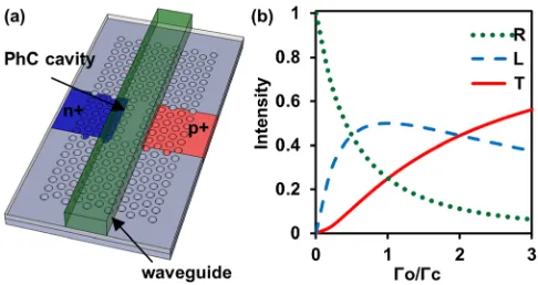
A schematic of the experimental realisation of our design is shown in Fig.1(a). It consists of a PhC cavity em-bedded into a pin diode. A Si3N4 based bus waveguide is
placed vertically above the cavity and separated by a buffer layer. This buffer layer acts as a physical separation between the waveguide mode and the cavity mode. Light is launched at one end of the waveguide and couples to the cavity mode when on resonance. Some of the coupled light is lost due to scattering/radiation loss or is absorbed in the cavity, while the remainder couples back to the waveguide mode contrib-uting to the reflection and transmission components in the waveguide. The coupling efficiency between the waveguide mode and the cavity mode can be optimized by maximizing the overlap between the k-space distributions of the two modes, as discussed in Ref.7. In the weak coupling approxi-mation, the transmittance (T), reflectance (R), and optical loss (L) on resonance can be expressed as8
FIG. 1. (a) Schematic of the device, where the defect implanted PhC cavity and the bus waveguide are vertically coupled through a buffer layer. An ar-bitrary PhC cavity is shown in the schematic for illustration purposes. The design of Ref.9is used in our experiment. (b) Theoretical plot of transmit-tance (T), reflectransmit-tance (R), and optical loss (L) againstCO/CCat resonance wavelength, using coupled mode theory.
a)
Electronic mail: [email protected]
[image:2.612.316.559.553.682.2]T¼ ðCOÞ
2
ðCOþCCÞ2
; R¼ ðCCÞ
2
ðCOþCCÞ2
; L¼1TR;
(1)
whereCCrepresents the decay rate of the cavity mode into
the waveguide mode, which corresponds to the coupling strength between the two modes and CO represents the
decay rate of the uncoupled cavity mode due to scattering/ radiation (CS) and/or absorption (CA) in the cavity, where
CO¼CSþCA. This holds for the standing wave case,8
which is appropriate for PhC cavities. As can be seen in Fig.1(b), T increases and R decreases with increasing CO/
CC. The optimum condition for photon detection occurs
whenCC¼CO and CACS. This corresponds to T and R
values of 0.25 (6 dB) with almost half (3 dB) of the inci-dent light being absorbed. This is the critical coupling con-dition but with a different form to that familiar from ring resonators (see Ref.8for a full discussion). Importantly, as long as the scattering loss is much lower than the absorption loss, an internal quantum efficiency of 0.50 may be achieved even with a weak absorber.
The PhC cavity design used here is a high quality factor cavity and is created by locally modifying the width of a W1 PhC waveguide.9As a result, bothCSandCAare very small
when defect-free silicon is used as the PhC cavity. By intro-ducing lattice defects in the cavity region, it is possible to increase the value ofCAwithout affectingCCandCS, and at
this point the optical loss will be dominated by defect-mediated absorption. Furthermore, by optimizing the con-centration of defects, it is possible to achieve CC¼CO,
which is the optimum situation for achieving maximum absorption and converting the maximum amount of incident light into photocurrent.
The fabrication process was identical to that of Ref.10, except for the additional defect implantation step. Following contact metallization, the devices were implanted with sili-con at 6 MeV and a dose of 31011cm2to introduce the lattice defects. The devices were tested optically by injecting light from a C-band Agilent tunable laser source into the nitride waveguides via butt coupling. The TE polarisation is selected using a polarisation beam splitting cube. Light was then collected from the other end of the waveguide via a col-limating lens coupler and passed via optical fiber to a detec-tor. The IV measurements were performed using a Keithley 6487 Pico ammeter/Voltage source connected to the chip via ground signal ground probe. This allowed for the photocur-rent generated to be measured for each wavelength while changing the reverse voltage. The wavelength/photocurrent scans were automated usingLABVIEW.
To observe the relationship between transmittance and photocurrent at the resonance wavelength, five different de-tector designs were realised by varying the k-space overlap between the waveguide and the cavity modes, thus varying CCin Eq.(1). We characterise the defect absorption by
moni-toring the transmittance (Eq.(1)); the transmittance was well below6 dB for the unimplanted devices, asCC dominates
overCO. After implantation, the absorption increases and so
do the cavity decay rateCO¼CSþCAand the transmittance,
untilCOandCCbalance. Figure2(a)plots the corresponding
functional relationship as well as the generated photocurrent for the five different devices with differentCCvalues. At the
implantation dose used here, the propagation loss due to defect absorption is approximately 20 dB/cm.11Before defect implantation, the Q-factors of the cavities were around 35 000, roughly corresponding to an equivalent propagation loss of 17 dB/cm. This loss arises mainly from scattering and free carrier absorption in the heavily doped regions of the pin diode. Thus, after silicon implantation, CO is dominated by
absorption loss as desired. It is clear from Eq. (1) and Fig.
2(a) that the maximum absorption occurs whenCC¼CO, in
which case the transmittance equals6 dB (0.25). In this op-timum situation, the maximum amount of light is absorbed and converted into photocurrent.
Figure2(b)shows the spectrum of the optical power in the waveguide immediately after the PhC cavity (this is cal-culated from the measured transmission spectrum using the known losses) and the generated photocurrent for a near-optimal device. On resonance, the transmittance is 0.30 and by comparing this with the theoretical values in Fig.1(b), we can estimate the total optical loss in the cavity to be 0.49 (3.1 dB). We then define responsivity as the ratio between the generated photocurrent and the total optical loss, which is 3.1 dB of the off-resonance optical power (45lW). For 0 V reverse bias, the generated photocurrent is 0.16lA which corresponds to a detector responsivity of 7 mA/W at resonance with a dark current of 0.5 nA. For a reverse bias of
10 V, the photocurrent increases to 2.1lA giving a respon-sivity of 95 mA/W, and the dark current becomes 9.4 nA. We note that the extinction ratio between the on-resonance pho-tocurrent and off-resonance phopho-tocurrent is maintained at 13.8 dB irrespective of reverse bias.
FIG. 2. (a) Blue dashed curve shows the theoretical relationship between transmittance and optical loss of the system at resonance. Red dots show the measured photocurrents for five different detectors with different transmit-tances. (b) Optical spectra in the Si3N4 waveguide immediately after the
PhC cavity (blue) and photocurrent at 0 V (in red) and10 V (in yellow) for the device with transmittance of 0.30. The off-resonance optical power is taken from the transmitted power spectrum well away from the resonance.
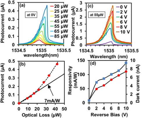
[image:3.612.317.555.51.296.2]Figure 3(a) shows the measured photocurrent versus wavelength, near the resonance wavelength as a function of the off-resonance optical power in the waveguide. The reverse bias is set at 0 V. As the optical power increases, we observe a redshift in the wavelength corresponding to the maximum photocurrent and also an asymmetry in the photocurrent response. We attribute this redshift to the thermo-optic effect caused by carrier recombination inside the intrinsic region of the diode. When the off-resonance optical power increases from 20lW to 85lW, the shift in resonance wavelength is 0.18 nm, which corresponds to a change in the cavity tempera-ture of2 K given the thermo-optic coefficient of silicon of 1.86104/K.12 In addition to thermo-optic detuning, we also note the effect of two-photon absorption, as is apparent in Fig. 3(b), where we plot the peak photocurrent against absorbed optical power. Here, two regions can be identified. For low power operation, the photocurrent increases linearly with absorbed optical power and follows a line corresponding to the 7 mA/W responsivity. As the absorbed power increases beyond 20lW, a second component with a quadratic depend-ence becomes apparent, which can be attributed to two-photon absorption.13,14 We believe that this behaviour is closely related to that observed in Ref.15.
We also investigated the effect of reverse bias on photo-current and resonance wavelength. The off-resonance optical power in the waveguide in this case was 55lW, with total optical loss of 25.3lW. Figure3(c)shows the measured pho-tocurrent as the reverse bias is increased from 0 V to10 V. For 0 V to 2 V, the photocurrent shows a sharp increase due to the fast sweep-out of photo-generated carriers from the intrinsic region of the diode and then a further (less dra-matic) increase with a reverse bias increase from 2 V to
10 V. As shown in Fig. 3(d), the responsivity increases with reverse bias from 9.5 mA/W to 108 mA/W, with a cor-responding increase in dark current from 0.5 nA to 9 nA.
These values are comparable to those reported for the best germanium photodiodes.16The effect of reverse bias on res-onance wavelength is particularly interesting. We first note a blueshift in the resonance wavelength when the reverse bias is increased from 0 V to2 V followed by a steady redshift for higher reverse voltage. For 0 V reverse bias, due to the lack of an external electric field, most of the photo-generated carriers recombine inside the intrinsic region and contribute to the rise in temperature of the cold cavity which causes a redshift of the resonance wavelength. As the reverse bias increases from 0 V to2 V, more of the photo-generated car-riers are swept away from the intrinsic region before they can recombine and the cavity temperature drops causing a relative blue shift in resonance wavelength. Further increases in reverse bias increase the photocurrent but cause Ohmic heating due to the movement of photo-generated carriers, redshifting the resonance wavelength once more. Using the same calculation used in the previous paragraph, we can esti-mate that a change in reverse bias of8 V increases the cav-ity temperature by 0.6 K.
Multiplexing and demultiplexing of multiple wavelength channels typically require use of complex arrayed waveguide structures (AWGs), Echelle gratings, or passive ring resona-tors. In the previous work,10 we have demonstrated that the vertically coupled waveguide-cavity architecture enables the multiplexing of multiple channels without the need for addi-tional wavelength selective components. Here, we use the same principle to achieve wavelength demutiplexing. Due to the wavelength selective nature of our detector, only one spe-cific wavelength channel will be detected. As a result, multi-ple detectors can be cascaded in series and coumulti-pled to the same waveguide. To demonstrate this functionality, we have cascaded two detectors to address two different wavelength channels, as shown in Fig. 4(a). To achieve different reso-nance wavelengths for the detectors, the cavities were fine-tuned lithographically, similar to Ref.10. Figure4(b)shows the normalized optical transmission spectrum (in blue) of the system, with each dip in transmission corresponding to a
FIG. 3. (a) Measured photocurrent spectra for different input optical power at 0 V reverse bias. (b) Measured photocurrent peaks as the absorbed optical power increases. The solid line corresponds to 7 mA/W responsivity and the dashed line shows the trend in photocurrent as the input power increases. (c) Measured photocurrent spectra for different applied reverse bias, when the input optical power is 55lW. (d) Measured responsivity (red circle) at reso-nance and dark current (blue square) as the reverse bias increases.
[image:4.612.53.297.493.696.2] [image:4.612.316.562.531.722.2]cavity. Red and yellow (dashed) curves show the detected photocurrent response from the first and the second detectors, respectively. The crosstalk for channel 1 from channel 2 is
7.2 dB and for channel 2 from channel 1 is8.5 dB. This approach shares many similarities with the previ-ous work on defect-mediated detection in ring resona-tors.6,17,18 While the Q-factor is similar in both cases, the finesse of the PhC cavity is significantly higher. This pro-vides a larger Free Spectral Range (i.e., the number of sup-ported channels) for the same Q-factor10 and allows a smaller device reducing the capacitance, by over an order of magnitude, and thereby the power consumption of subse-quent electronic amplifiers. Similar to Ref.10, by avoiding the use of spot size converters, grating couplers, AWGs, or Echelle gratings, a significant reduction in the optical power budget is also possible, which is very promising for on-chip networks.19 This brings the effective responsivity (photo-current relative to power from the optical fibre) of our photodiode much closer to the III-V/Germanium demulti-plexed photodetection systems. Alternatively to operating as a photo-detector, the system could be considered for moni-toring light propagating in a dielectric waveguide, avoiding the need for tap-off and spot size converting structures. Further optimisation of the implantation dose and coupling conditions will lead to improvements in the responsivity. Improvements in the pin junction layout and the use of sidewall passivation will also improve the extraction of photocarriers. The nonlinear dependence of responsivity in Fig. 3(b) indicates that further improvements in coupled power can lead to significant enhancements of the responsiv-ity. This is related to the device of Ref.13, though we use lower and more practical Q-factors.
In summary, we have demonstrated wavelength selective photo-detection in deep-level mediated silicon photodiodes. Due to the high optical confinement achievable in PhC cav-ities, the detector size can be reduced considerably in com-parison to silicon waveguide based devices. Additionally, vertically coupling to low refractive index waveguides pro-vides very low insertion losses and access to powerful passive optical components. By cascading multiple cavities along the
same waveguide, a simple and elegant photo-detection scheme may be realised, which is the ideal counterpart to the modulator architecture of Ref.10.
This work was supported by EPSRC under the UK sili-con photonics project and through the EraNET Nano-Sci project LECSIN. The authors would like to thank Andrea Melloni and Emel Tasyurek for useful discussions.
1D. A. B. Miller,Proc. IEEE97, 1166 (2009).
2H. Park, A. W. Fang, R. Jones, O. Cohen, O. Raday, M. N. Sysak, M. J.
Paniccia, and J. E. Bowers,Opt. Express15, 6044 (2007).
3
L. Vivien, J. Osmond, J.-M. Fedeli, D. Marris-Morini, P. Crozat, J.-F. Damlencourt, E. Cassan, Y. Lecunff, and S. Laval,Opt. Express17, 6252 (2009).
4
A. P. Knights, J. D. B. Bradley, S. H. Gou, and P. E. Jessop,J. Vac. Sci. Technol. A24, 783 (2006).
5M. W. Geis, S. J. Spector, M. E. Grein, R. T. Schulein, J. U. Yoon, D. M.
Lennon, S. Deneault, F. Gan, F. X. Kaertner, and T. M. Lyszczarz,IEEE Photon. Technol. Lett.19, 152 (2007).
6
J. K. Doylend, P. E. Jessop, and A. P. Knights,Opt. Express18, 14671 (2010).
7K. Debnath, K. Welna, M. Ferrera, K. Deasy, D. G. Lidzey, and L.
O’Faolain,Opt. Lett.38, 154 (2013).
8
Y. Xu, Y. Li, R. K. Lee, and A. Yariv,Phys. Rev. E62, 7389 (2000).
9K. Welna, S. L. Portalupi, M. Galli, L. O’Faolain, and T. F. Krauss,IEEE
J. Quantum Electron.48, 1177 (2012).
10
K. Debnath, L. O’Faolain, F. Y. Gardes, A. G. Steffan, G. T. Reed, and T. F. Krauss,Opt. Express20, 27420 (2012).
11P. J. Foster, J. K. Doylend, P. Mascher, A. P. Knights, and P. G. Coleman.
J. Appl. Phys.99, 073101 (2006).
12
S. A. Clark, B. Culshaw, E. J. C. Dawnay, and I. E. Day,Proc. SPIE3936, 16–24 (2000).
13T. Tanabe, H. Sumikura, H. Taniyama, A. Shinya, and M. Notomi,Appl.
Phys. Lett.96, 101103 (2010).
14
R. Hayakawa, N. Ishikura, H. C. Nguyen, and T. Baba,Appl. Phys. Lett.
102, 031114 (2013).
15B. Vest, E. Lucas, J. Jaeck, R. Haidar, and E. Rosencher,Appl. Phys. Lett. 102, 031105 (2013).
16
C. T. DeRose, D. C. Trotter, W. A. Zortman, A. L. Starbuck, M. Fisher, M. R. Watts, and P. S. Davids,Opt. Express19, 24897–24904 (2011).
17D. F. Logan, P. Velha, M. Sorel, R. M. De La Rue, A. P. Knights, and
P. E. Jessop,IEEE Photon. Technol. Lett.22, 1530 (2010).
18
K. Preston, Y. H. D. Lee, M. Zhang, and M. Lipson, Opt. Lett.36, 52 (2011).
19A. Biberman, K. Preston, G. Hendry, N. Sherwood-Droz, J. Chan, J. S.
Levy, M. Lipson, and K. Bergman, ACM J. Emerg. Technol. Comput. Syst.7, 7 (2011).