A Light Direction Sensor
for Integrated 3D Vision
Robin Buijs
16 January, 2015
Abstract
About this work
The work described in this document is part of the Dutch NWO/STW VENI project “Controlled three-dimensional self-assembly of silicon nanoparticles using hydrogen bonds” led by Dr. Léon A. Woldering. It is embedded within the Transducers Science & Technology group within the MESA+ Institute for Nanotechnology of the University of Twente, led by Prof. Dr. Gijs J.M. Krijnen. The work was performed in partial fulfilment of the MSc programmes in Applied Physics and Electrical Engineering at the University of Twente, and jointly supervised Prof. Krijnen and Prof. Dr. Willem L. Vos of the Complex Photonic Systems chair, also part of the MESA+ Institute. Independent supervision was done by Prof. Dr. J. Schmitz of the Semiconductor Components group in the same institute.
This work builds on years of experience within the TST group, as well as valuable input from the COPS group and several others. All four supervisors have contributed a wealth of expertise. Several members of the TST group have provided help in topics ranging from measurement en-gineering to wirebonding. The COPS group members have contributed in regular discussions and spectrometry. The MESA+ Cleanroom staff have played a large role in fabrication process engin-eering and optimisation. Prof. Dr. J.J.W. Van der Vegt of the Numerical Analysis & Computational Mechanics group has provided advice on Green’s function theory.
I owe my thanks to all these people for having provided me the opportunity to do high-level science and engineering in a highly professional and ambitious environment. In addition, I thank my direct colleagues in the TST and COPS groups for a social environment that helps make science even more enjoyable.
STW is gratefully acknowledged for funding.
Transducers Science & Technology group MESA+ Institute for Nanotechnology University of Twente
P.O. Box 217 , 7500 AE Enschede , the Netherlands
Complex Photonic Systems chair MESA+ Institute for Nanotechnology University of Twente
Contents
1 Introduction 1
1.1 The light field . . . 2
1.2 Light direction sensing . . . 2
1.3 3D structured detector . . . 4
2 Detector design 6 2.1 Anisotropic etching . . . 6
2.2 Light detection . . . 7
2.3 Metal-semiconductor contacts . . . 9
2.4 Pit-based detector . . . 10
2.5 Tetrahedron-based detector . . . 11
3 Detector modelling 14 3.1 Excess carrier dynamics . . . 14
3.2 Resistor modelling . . . 22
3.3 Pit-based detector . . . 26
3.4 Tetrahedron-based detector . . . 28
3.5 Colour vision . . . 30
3.6 Materials requirements . . . 31
3.7 Discussion . . . 33
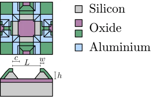
4 Materials properties validation 35 4.1 Sample design . . . 35
4.2 Fabrication . . . 36
4.3 Experimental results . . . 38
4.4 Discussion . . . 40
5 Detector realisation 41 5.1 Design specification . . . 41
5.2 Process outline . . . 42
5.3 Results . . . 45
5.4 Discussion . . . 46
6 Light direction sensing setup 49 6.1 Light source . . . 49
6.2 Sample holder & probe mount . . . 50
6.3 Measurement engineering . . . 51
6.4 High-ohmic measurements . . . 53
6.5 AC vs DC operation . . . 53
6.6 Temperature management . . . 53
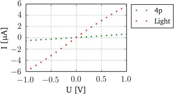
7 Light direction sensing results 55 7.1 Results . . . 56 7.2 Discussion . . . 59
8 Conclusions & Outlook 61
A Electromagnetic waves 63
B Semiconductor optics 65
C Green’s functions for the diffusion equation in three dimensions 67
Chapter 1
Introduction
Visual depictions of reality form a staple of human culture. In modern times, photography and video have found major roles in communication, from personal interaction to scientific research.
Most cameras are built according to one particular layout. A set of optics, also referred to as the objective, maps the incoming light rays to a sensor plane. There the spatial intensity distribution is recorded, either photochemically or in discrete electronic pixels. The optical system directs light coming from a point on the subject plane to a single point at the sensor. Points farther away from this plane are increasingly blurred.
The rate of blurring with distance is inversely measured by the depth of field. The depth of field increases with smaller apertures, but this also limits the amount of light reaching the sensor. Taking a photograph thus requires compromising on what parts of the scene will be imaged well.
In addition to the basic optics-sensor system, a complete camera features several components to help in the creative process. A simplified schematic of the sophisticated single lens reflex camera is shown in figure 1.1. Here, a set of movable mirrors is used for user feedback and possibly to direct some light to a separate sensor for an auto-focusing system. The detector housing contains additional optics to introduce colour vision and refocus for optimal detection. [1]
Interestingly, conventional cameras record only a fraction of the information in the light incid-ent upon their sensors. Each pixel integrates the light it receives to a local light intensity. The light direction distribution is irretrievably lost. How this affects photography is better understood in terms of the light field.
1.1
The light field
In the limit of geometrical optics, light may be taken to travel in rays.[34] A ray originates from a light source and travels along a fixed direction until encountering an obstacle, where secondary rays may originate. Each such ray is fully described by a position along its lengthx, y, z, its direc-tionsθ, φand its radianceL. We can express radiance as a function of the other variables. This is the full five-dimensional light fieldL(x, y, z, θ, φ).1[2]
A camera sensor pixel has a fixed position in space. The information such a pixel can conceiv-ably extract from the light field is then the light intensity in each possible direction, orLx,y,z(θ, φ).
Ordinary camera pixels integrate this function over all angles to find a single radiance for each pixel,Leff =
RR
L(θ, φ)dθdφ.
Finding the complete reciprocal space spectrum of the light source is conceptually interesting, as it allows full lensless imaging through Fourier analysis. However, this would require the record-ing of a huge amount of information per pixel. A simpler approach is to define a srecord-ingle overall, effective light direction for each pixel.
We can express the radiance with its effective direction either in three variables, or in a single vectorLx,y,z. This vector describes the net energy flux through some point in space and is identical
to the Poynting vector in electromagnetism.[10] If, as per usual, there is a well-defined sensor plane (z= 0), we can combine the information in the individual pixels into the effective light field at the sensorL(x, y).
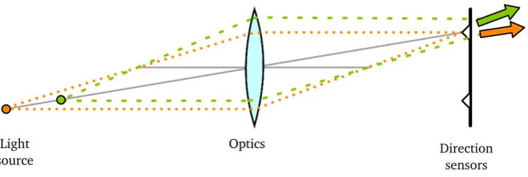
The power of this approach is visible in figure 1.2. We consider a pixel that can resolve radiance and light direction. Two objects are positioned along the same line through the centre of the optical system and as such in principle mapped to the same pixel - although of course at least one is out-of-focus.
For the out-of-focus light source, only a specific subset of reciprocal space vectors arrives at the sensor: in case of fore-focus, the most oblique rays miss the pixel, while in case of rear-focus the least oblique ones miss. The effective light direction thus varies smoothly and monotonously with distance to the light source. This means that the light direction sensor directly measures distance to the light source.
The implications for photography are enormous. Knowledge of the third dimension allows manipulation of both focal length and depth of focus. The direct recording of depth information enables the reconstruction of the three-dimensional scene in any desirable format in a single sensor.
1.2
Light direction sensing
A device capable of exploiting these properties of the light field is called a light field, or plenoptic, camera. The principle by which commercially available light field cameras operate was proposed in the early 20th century. [3] It is illustrated in figure 1.3.
The camera may use an ordinary light intensity sensor array, but between it and the objective, a microlens array is placed so that each microlens covers a number of pixels. The light incident on the microlens is refocused and passes on to the sensor. The local intensity pattern on the sensor is a measure for the focal error, so that 3D-information on the scene can be retrieved for the region corresponding to each microlens. For large focal error the pattern tends to uniformity, so that in practice, multiple microlenses with different focal lengths may be used to obtain a good resolvable depth range. [4]
1In empty space, one of the dimensions is redundant, because the entire field can be reconstructed from a single
Figure 1.2: Two light sources, positioned such that they are mapped to the same pixel, give differ-ent readings on the direction sensor. Since the effective direction of the light field on the pixel is a smooth, monotonous function of focal error, the distance to the light source is measured directly.
This technique has an obvious drawback in that spatial resolution is limited to one effective pixel per microlens. The two major commercial camera manufacturers report a minimum resol-ution loss of a factor of4 and10compared to the native resolution of the sensor. [4][5] A low number of pixels per microlens however limits the range of focal error that can be resolved. Note also that this technique can only resolve the focal error of the incident light; it does not actually detect light direction, limiting its possible uses.
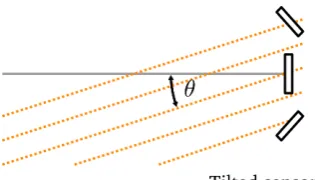
Several means of detecting light direction have been proposed. One example with classical roots is shown in figure 1.4. Here, use is made of the fact that the radiant flux through a surface depends on its angle with the incoming radiation. If two surfaces under different angles are com-pared, radiance and one dimension of incoming light direction can be resolved. Another surface under a yet different angle fixes the second direction.
This principle is used on the microscale in phase-type autofocus systems. Here, photodiodes are mechanically mounted under alternating angles. Each angle looks towards one aperture. If the image is in focus, light through each aperture will reach the centre of the sensor. If it is out-of-focus, the two beams will move apart. The direction sensors can tell which beam is on which side and thus both the sign and magnitude of focal error. This technique is however limited to applications where the relatively high price per pixel is not an issue, because the requirement of mounting separate diodes makes for a complicated assembly process. [1]
[image:11.595.109.491.96.224.2]Another example with a long history is the sundial, where the position of the shadow of an
Figure 1.4: Tilting a sensor with respect to the local radiance vector will change the radiant flux it perceives. This effect can be used to find light direction from two sensors under different angles. In this image, the middle sensor receives less light than it would at normal incidence, and the lower sensor receives less yet. The upper sensor, however, receives more light than at normal incidence, because from its perspective the light is moving towards normal.
object measures the incoming light direction. Microscale variations have been proposed, but suffer either from very low resolution or lack of radiance sensitivity despite a complex fabrication process. [6] [7]
A more advanced recent proposal uses the Talbot effect of near-field diffraction to obtain a light direction dependent light intensity in the sensing region behind a pair of gratings. Combining the information of several of these sensors allows one to resolve the full radiance vector. Its prime disadvantage is the need to combine several sensors, all of which need to be many wavelengths in dimension, leading to aliasing in the measured signal. In addition, no more than half the light ever reaches the sensing region. [8]
1.3
3D structured detector
In this work we investigate the possibility of integrating multiple light-sensitive surfaces under different angles on the same microstructure. Such a structured detector would have all the advant-ages of the tilted sensor-approach, but not the drawback of complicated assembly.
We investigate two types of structures, indicated in figure 1.5. In the pit-based detector the tilted surfaces are the sloping regions of a depression in the detector surface. The tetrahedron-based detector uses a monolithic protrusion from the surface, where each surface is a separate sensing plane.
(a) (b)
Chapter 2
Detector design
From the principle of three-dimensional detector structuring a qualitative design for a detector can be made. Three further technological feats are required to define a detector outline in appreciable detail.
We will discuss the technique of anisotropic etching, with which three-dimensionally structured surfaces can be produced, the different methods of light detection in semiconductors and the theory of metal-semiconductor contacting, before moving on to the detector designs.
2.1
Anisotropic etching
The different planes in a crystal, when exposed to the environment, will undergo different re-constructions to fix the dangling bonds. Each such reconstruction is chemically distinct. For this reason, certain chemicals show very different etch rates on different surface planes. This can be exploited for a process known as anisotropic etching.[9]
Silicon natively forms an FCC diamond lattice with a two-atomic basis. The <100> plane is most commonly used as substrate surface. Tetramethyl ammonium hydroxide (TMAH) is one of several etchants that etch the <100> plane selectively with respect to the <111> plane. The selectivity of <100> over silicon dioxide and silicon nitrides is higher still, meaning these can be used as masks.[9] The result is that a square window in an oxide layer on <100> silicon, oriented along the <100> direction, can be etched down to an inverted square pyramid. On wafers with a buried oxide, known as SoI wafers, larger pits may be capped of by the oxide.
The process is to a large degree self-limiting. After all the available <100> silicon has been etched down, leaving only <111> faces exposed, etching of these planes still goes very slowly. This technique can thus be used to create a range of three-dimensional surface structures with a relatively simple, robust process. This is illustrated in figure 2.1.
The angles involved can be found directly from the symmetry of the diamond lattice. The eight planes with Miller indices(±1,±1,±1)are identical by symmetry. Planes differing by two signs form part of the same regular tetrahedron. The geometry of a tetrahedron is shown in figures 2.2 and 2.3. It can be seen that the angle between a plane and an edge, which is the angle between the <100> and <111> planes, isθ= 54.74◦.
Figure 2.2: The locations of the vertices of a tetrahedron in a straightforward coordinate system.
(a) (b)
Figure 2.3: (a) top view of a tetrahedron. (b) cross-section of a tetrahedron along the line drawn in (a). Note that the faces make an angle ofθ= 70.53◦with one another. The angle ofθ= 54.74◦
is between an edge and the plane at either end.
On SoI wafers, the etch can also be used to make electrical islands in the device layer. However, corners of the silicon pointing outwards do not simply etch down to the <111> plane. This can be seen in figure 2.4. Without going into detail we note that this etch rate is about three times as large as the <100> rate, so that any outer corners will need significant leeway to not be destroyed during etching.
2.2
Light detection
Figure 2.4: An anisotropically etched channel in silicon making a straight corner. The outer corner of the remaining silicon is visibly etched more quickly than the rest of the structure.
Semiconductors are materials with electronic states both somewhat above and somewhat below the Fermi energy, but none close to it. As empty states are required for conduction, the only carriers that contribute to conduction are those excited over this gap, known as the bandgap, by thermal effects or other energy in the system. In addition, the introduction of impurities known as dopants can introduce extra electrons to the higher-energy band, or remove them from the lower-energy band, leaving electron holes.
Absorption of incident light in a semiconductor will generally cause some combination of heat-ing and excitation of electrons, leavheat-ing an electron-hole pair. The balance between the two depends on photon energy.
The band gap of silicon isEg = 1.1 eV[13]. This means that visible light has plenty of energy
to overcome the band gap, and light more energetic thanλ= 564 nmhas enough energy to excite two photons.
At one excitation per absorbed photon1we can calculate the excess carrier generation rate as a function of incident light intensity.
The difference between photovoltaic detection and photoconductive detection is in the way the carriers are separated.
A photodiode has a depletion layer where few free carriers remain in the face of a built-in voltage. Excess carriers generated here will naturally drift off, and given their opposite signs, drift off in opposed directions. These extra carriers will then contribute to building up an external potential difference. This is the photovoltaic effect.
In practice, the photodiode is shorted through a current meter. The current then directly meas-ures the carrier generation rate.
The photoconductive method lacks the built-in voltage and thus needs to apply an external voltage to separate the generated carriers.
Semiconductor conductivity depends on carrier concentrations through
σ=e(µen+µhp) (2.1)
whereeis the elementary charge,nandpare carrier densities andµthe corresponding mobilities. These non-equilibrium carriers have a fixed lifetimeτ, which together with the generation rate
Gleads to a fixed increase in their concentrations. They contribute to conductivity as any other in
equation 2.1, giving rise to a conductivity change
∆σ=e G(µeτe+µhτh) (2.2)
At a fixed external voltage, the current measures the generation rate here too.
Although photovoltaic detection is industry standard and more interesting for commercial devices, photoconductive detection makes for an easier fabrication process, negating the need for active doping, and preserves the symmetry of the system.
In addition, given the close relation between the two, it is entirely to be expected that insight gained from photoconductively operated devices is directly applicable to photovoltaically operated devices.
We thus decide to use the photoconductive effect as the mode of operation of the detectors under design.
2.3
Metal-semiconductor contacts
φm< φs φm> φs
n Ω D
i Ω? Ω?
p D Ω
Metal-semiconductor junctions can behave as either Schottky diodes or Ohmic contacts depending on the spe-cific materials properties.[13]
A basic theoretical description can be phrased in terms of work functions and doping. On contact, elec-trons will flow from the semiconductor’s conduction
band into the metal, while the metal’s electrons will fill up the electron holes in the semicon-ductor’s valence band. If the numbers of these charge carriers are not in balance due to doping, a space charge will develop around the interface to prevent further depletion. The band structure will curve to reflect the inhospitality to one type of charge carrier, with a barrier height determined by the difference in work functions. If majority carrier depletion would occur in the semiconductor, a barrier is formed. Carrier depletion in the metal does not significantly alter the net concentration or conductivity, leaving an Ohmic contact.
The same statement can be phrased in terms of band diagrams. The difference in work func-tions represents a difference in Fermi energies before contact. When contact is made, the bulk band levels shift with the Fermi level, but near the interface they retain their old value to accommodate the space charge. If this curvature provides a barrier for the majority carrier in the semiconductor, no current will flow from the semiconductor into the metal.
The theory suggests that contacts with intrinsic semiconductors would be Ohmic no matter what, because only one type of carrier can be obstructed at the same time. However, very light doping - including interface effects - could already make the junction rectifying. Tables of work functions by metal and electron affinityχ plus band gapEG by semiconductor are known from literature.[13] For silicon, the work function can be calculated to beφ= 4.61 +dφeV, withdφa small correction for the shift in Fermi level due to doping.
Considering experimental artefacts, the best metals would be those with a large safe margin
∆φin the work function. For n-doped silicon, the best common metals for contacting would be thorium (∆φ <1.0 eV), aluminium (∆φ <0.5 eV) and copper (∆φ <0.3 eV). For p-doped silicon, the best options would be platinum (∆φ <1.5 eV), gold (∆φ <0.2 eV) and silver (∆φ <0.1 eV).
In real systems, junction behaviour is very different. Highly doped contacts are Ohmic no matter what, because the small depletion length is easily traversed by tunnelling with disregard for junction details.
In addition, interface effects tend to near-completely drown out the above theory.[23] This is theorised to be caused by electronic gap states caused by the dopants. Contacts are also very much affected by local doping from the contact material.
One additional consideration is that highly reactive2metals, such as aluminium, will chemically react with a native oxide, improving adhesion and leading to a much better contact. As such,
Table 2.1: The bandgap EG and electron affinity χ of selected semiconductors, and the work functionφof selected metals. Data reproduced from [13]
EG(eV) χ(eV) GaAs 1.43 4.07
AlAs 2.16 2.62
GaP 2.21 4.30
InAs 0.36 4.90
InP 1.35 4.35
Si 1.12 4.05
Ge 0.66 4.00
φ(eV) Al 4.1
Cs 1.9
C 4.8
Cu 4.3
Au 4.8
φ(eV) Fe 4.6
Pt 6.3
Ag 4.7
Th 3.5
W 4.5
aluminium is claimed to make acceptable contacts on both n- and p-doped silicon.[24][25] In its pure form, aluminium is known to disturb the silicon lattice and form spikes into it, possibly leading to a device failure mode known as as junction spiking. To counter this, 1% silicon is sputtered along with the aluminium. Expert advice from MESA+ cleanroom staff supports this technique for aluminium-silicon contacts without any annealing steps.
Commercially, heavy use is made of contact layers to improve contact. This normally has the obvious drawback of introducing extra process steps.
Considering the difficulties in contacting semiconductor material with metal directly, it may be more practical to construct the leads to the detector from highly doped semiconductor. When both materials have the same majority carrier this should produce very nice contacts. The problem of metal-semiconductor contacting is then moved to a point further from the detector, where space is not an issue - allowing for larger contact area - and very high doping can be employed to make good contact with any type of metal.
One possible fabrication method involves depositing polycrystalline silicon on the whole wafer and implanting abundant dopants at a certain depth. The excess poly-silicon can the be etched away with a Wright etch.
A perk of this method is that the poly-silicon can also act as a getter for impurities in the detector material. One drawback is that the Wright etch is rather toxic.
For an initial design, silicon-infused aluminium appears the best choice.
2.4
Pit-based detector
With the previously discussed considerations, we aim to design a photoconductive light direction sensor based on an anisotropically etched pit in <100> silicon.
The detector is to function by comparing the resistance changes due to light caught in the silicon behind different <111> surfaces. To minimise detector size, it makes sense to use the inside surfaces of a pit. A single square pit has two pairs of opposing faces and the radiant flux pattern directly measures the fullLx,y vector.
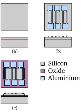
If we consider one such a pit on a large, otherwise mirrored island, with contact leads to the corners of the pit, we have a detector, albeit not a very good one. This design is shown in figure 2.5. Already, a few tradeoffs have been made; the mirroring, for example, contains faults, to prevent shortage between the contacts.
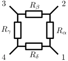
We can model the pit-based sensor as a four-resistor ring as n figure 2.6. Each measurement between two contacts is affected by all resistance values, but most strongly by the resistor directly between the contacts.
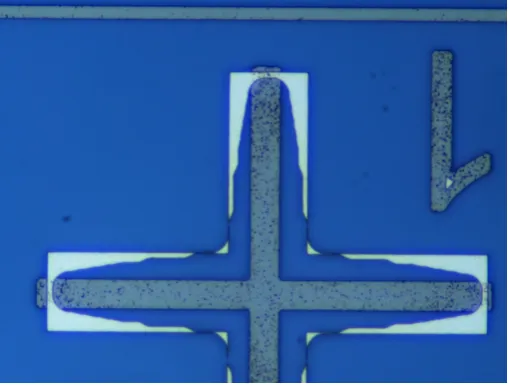
Figure 2.5: Schematic top view and cross-section of a very basic pit-based detector design. The central pit has four tilted surfaces that catch light. Light entering from other sides is precluded by the large aluminium mirrors. The resulting resistances are read out through the aluminium contacts in the corners of the pit.
Figure 2.6: The four-resistor equivalent model of the pit-based detector. Contact resistances are not shown.
A more advanced general design is shown in figure 2.7. The resistors behind the light-sensitive surfaces are now of limited and well-defined dimension, so that the relative conductance change due to lighting is as large as possible.
Additionally separate current contacts have been added, so that four-point measurements may be used.
The mirroring is imperfect, but insulated overlapping mirrors would require a much more com-plicated design.
2.5
Tetrahedron-based detector
An anisotropic etching process to fabricate regular tetrahedra in the <111> device layer of a SoI wafer was designed in earlier work.3 It leaves silicon tetrahedra regularly spaced on the buried oxide layer of a SoI wafer.
Contacting these tetrahedra is relatively straightforward, as seen in figure 2.8. Given the small desired dimensions of the system however there is no clear way to introduce separate sense con-tacts. This approach thus depends on the viability of two-point measurements.
The tetrahedron too can be represented as a resistor ring. As all considered effects are linear, there must be some way to express it as a linear electronic circuit. In the steady state, when only the base vertices are considered, a three-resistor model, as in figure 2.9, can describe all the
Figure 2.7: A more advanced pit-based detector. The measurement channels are narrower to maximise the relative effect of incident light. Separate source and sense contacts are implemented to allow characterisation of only the channel properties.
Figure 2.8: A basic contact layout for the tetrahedron-based detector. The tetrahedron fabrication process is documented elsewhere. Four-point contacting of the tetrahedron is likely to be infeasible due to the small size.
Chapter 3
Detector modelling
We aim to quantify the expected behaviour of the detectors designed in chapter 2 as a function of the remaining design parameters. The design can be fine-tuned based on such a model. The model can also help interpret measurement data.
One major theoretical challenge is the behaviour of excess carriers within the devices. When the conductivity profile is clear, we need a way to translate this to a resistance. Then, we would like to relate this resistance to the resistances we measure. The lessons learnt here will result in a set of requirements on the substrates to be acquired for device fabrication.
3.1
Excess carrier dynamics
As discussed in chapter 2, the photoconductive effect leads to a conductivity change of
∆σ=e G(µeτe+µhτh) (3.1) withethe elementary charge,Gthe carrier generation rate,µelectronic mobilities andτ excess carrier lifetimes.
The carrier generation rate is determined by the incident radiant flux and the quantum effi-ciencyηof the photoelectric effect. This has been studied in detail by others.[14] For us it suffices to note that this value varies betweenη = 0.5andη= 0.8, staying close toη= 0.7for much of the visible spectrum.
In a wafer of any detectable doping, the majority carriers fully determine conductivity. The mobility for holes in a lightly doped p-type semiconductor near room temperature is [15]
µh=µmin+
µ0
1 + (N/Nref)α
= 4.612×10⁻²m
2
V s
The lifetime of excess carriers is set by the availability of minority carriers to recombine with. Although the lifetime of majority carriers is much longer, because their chances of meeting a minor-ity carrier are quite small, the excess concentration will decrease as quickly as the minorminor-ity excess. Effective minority carrier lifetime is mostly determined by the presence of crystal defects, in-cluding both dopant atoms and the crystal edge. Aside from this qualitative observation its value is hard to predict and hard to modify. [17]
For the bulk lifetime of silicon wafers, literature estimates range betweenτ= 10−1000µs.[19][16] A value ofτ= 100µswill be considered reasonable for this type of sample. However, in most sys-tems steady-state concentrations are strongly affected by surface effects. For macroscale syssys-tems, an effective lifetime can be defined to describe the overall statistics of the carriers,
1 τeff
= 1
Surface lifetime is determined by the diffusion current reaching the surface and the recombin-ation rate on the surface, normally expressed in a recombinrecombin-ation velocityS in m3
m2s. On untreated silicon the recombination velocity is tiny. This limits effective lifetimes in wafers of thickness
lw= 300µmto aboutτ = 2.5µs. However, surface lifetime can be vastly increased by passivation, for example through growth of a thermal oxide. Note that silicon will readily grow a native oxide, so that recombination velocity may decrease significantly without active processing.
The floating zone (FZ) crystal growth process is an alternative for the standard Czochralski (CZ) process. The FZ process leads to significantly lower impurity concentrations and is known to produce much higher bulk lifetimes and thus efficiencies in photovoltaic devices; practically obtainable efficiencies currently go up to aboutη= 25%for FZ-grown silicon versusη= 20%for CZ-growth. [17] [18]
3.1.1
One-dimensional systems
We will analyse the behaviour of excess carriers in one-dimensional resistors. Consider light of monochromeλ= 500 nmat an intensity ofI= 1 W
m2
1that is fully absorbed at quantum efficiency
η = 0.5over z = 1.0µm into some area A. Writing generation ratesr, we would see an excess generation of
G=rphotons V relectrons rphotons = P Ephoton
Az η= IA hf η Az = 1 hf η I
z = 1.26×10
24 1
m3s = 1.26×10 18 1
cm3s
with, usingτh= 100µs, a predicted change in conductivity of
∆σ=e G µhτh
= 9.2×10⁻¹ 1
Ωm
on an unperturbed conductivity of about
∆σ=e µhp
= 8.3×10⁻³ 1
Ωm
forp= 1×1012cm13 leading to a net resistivity change fromσ−1= 120Ωmtoσ−1= 1.1Ωm.
The conductivity change scales linearly in carrier lifetime and generation rate. This means that as long as this equation did not overestimate their product by more than four orders of magnitude, the change in resistivity will be more than1%.
A more realistic approach treats the generation rate as a function of depth. Absorption in the material leads to the skin depthls, a length scale for the reduction in wave energy, as discussed in appendix B. SinceI∝ e−lzs we have
G(z) =rphotons V
relectrons
rphotons
=dNphotons A dz η=
η hf dI dz = η hf I(z)
ls
An additional effect is that carriers on the surface will recombine exceedingly rapidly due to the huge crystal defect the surface represents. Carriers from the bulk will tend to diffuse towards this region where no excess carriers exist.
Figure 3.1: Excess carrier concentration profiles in a semi-infinitely thick wafer. Concentration is shown versus depth in the material. The skin depth and the diffusion length provide two relevant length scales. At low carrier lifetimes diffusion has a small effect, but concentrations are small anyway due to the same small lifetimes.
Considering photogeneration, recombination and diffusion we then have two equations for carrier concentration. The first is simplyc= 0at the surface. The second is
dc dt =
η hf
I(z) ls
−c τ +D
d2c
dz2 (3.2)
This can be solved in the steady state, where dc
dt = 0. Using a minority carrier diffusion length ld=√D τ,2
c(z) = η hf
τ I0
ls(1−
l2
d
l2
s)
(e−lzs − e−
z
ld) (3.3)
Note that for vanishing diffusion length, this reduces to the generation rate. Differentiation shows that the concentration peaks atz= ldls
ld−lslog
l
d
ls
. The peak value increases with diffusion length.
This solution does not work forls=ld; there,c(z) = η τ Ihf0
z lse
−z ls
2ls which neatly peaks atz=ls.
The curves for a set ofld/lsratios are shown in figure 3.1.
Equation 3.3 is not the only mathematical solution to the diffusion equations, as multiples of e−lzd − elzd can be added at will. In the present system however any such addition leads to a non-physical solution, as the positive exponential implies ever-increasing carrier concentrations at largez.
In a system of finite thickness, the situation is different. Neglecting reflection at the back plane, we have the same diffusion equation 3.2. For boundary conditions we have at the front plane still
c(0) = 0, but now alsoc(lw) = 0.
We can now use the free parameter in the previous solution to settle the second boundary condition, resulting in
c(z) = η hf
τ I0
ls(1−
l2
d
l2
s)
e−zls −e−
z ld +e
−lw
ld − e−
lw
ls
ellwd −e−
lw
ld
(elzd − e−
z ld)
!
(3.4)
Figure 3.2: Excess carrier concentration profiles in a wafer of finite thickness. Concentration is shown versus depth in the material. There are three relevant length scales here. Skin depth and sample thickness are fixed atlw/ls= 10.0. This image may describe anlw= 5µmsample at green light, wherels ≈500 nm.
Figure 3.3: The effect of light colour on excess carrier concentration profiles, otherwise like figure 3.2. The curves represent red (λ = 630 nm), green (λ = 500 nm) and blue (λ = 450 nm) light respectively. Diffusion length is kept constant at ld = 10µm while wafer thickness is fixed at
A more systematic approach to solving these types of problems uses Green’s functions, a type of function that characterises the differential operator. We are interested in a functionG(r)that satisfies
L G(r) =−δ(r)
using Dirac delta functionδ.
From the Green’s function, the steady state charge carrier distribution can be calculated through
c(r) =χ(r) +
Z Z Z
G(r−r0)f(r0)d3r0
where the rightmost term is called the source term and represents the external perturbation onc.
χis a solution to
L χ(r) = 0
and generally allows some freedom to satisfy boundary conditions.
We try to reproduce the above result using the Green’s functions technique. The equation to be solved is dc dt = η hf I0 ls e−lzs −
c τ +D
d2c
dz2 (3.5)
or, in the steady state,
L c+f(z) = 0
with L= d
2
dz2 −
1 l2 d
f(z) = η hf τ l2 d I0 ls e−lzs
This equation can be transformed to momentum space as
F
d2
dz2G(z)−
1 l2 d
G(z)
=F(−δ(z))
(−k2− 1
l2d)G(k) =−1 G(k) = 1
k2+ 1
l2
d
Direct inverse Fourier transformation then gives3
G(z) =F−1 1 k2+ 1
l2
d
!
= ld
2 e
−|z ld|
2The diffusion constantDfor a particle of chargeecan be found from electrical mobilityµusing the Stokes-Einstein
relationD=µ kBT /e. 3This is evident as
F
e−|
z ld|
=
Z
e−|
z
ld|eikzdz=
Z 0
−∞ e
z
ld+ikzdz+
Z ∞
0
e−
z
ld+ikzdz= 1
1
ld+ik
+ 1 1
ld−ik
= 2
ld
1
k2+l2
We can also solve
L χ(r) = 0 χ(z) =c1e
z ld +c
2e −z
ld
We first calculate the source term,
c(z)−χ(z) =
Z lw
0
G(z−z0)f(z0)dz0 | f(z) = η hf τ l2 d I0 ls e−lzs
= η hf τ l2 d I0 ls ld 2
Z lw
0 e−
|z−z0 | ld e−
z0 lsdz0
= 1 2 η hf τ ld I0 ls " Z l 0
e−lzd+z
0
ld−z
0
lsdz0 +
Z lw
l
elzd−z
0
ld−z
0
lsdz0
#
= 1
2 η hfτ I0
1 ls
1
1−l2d
l2
s
2e−lzs −[1 +ld
ls
]e−lzd −[1−ld
ls
]e−llwd e−
lw
ls e
z ld
and using the known form ofχexplicitly write the excess carrier concentration
c(z) =c1e z ld +c
2e −z
ld +1
2 η τ I0
hf 1 ls
1
1−l2d
l2
s
2e−lzs −[1 +ld
ls
]e−lzd −[1−ld
ls
]e−llwd e−llws e
z ld
˜
c(z) = ˜c1e z
ld + ˜c2e−
z ld +e−
z ls −
1 +ld
ls
2 e
−z ld −
1−ld
ls
2 e
−lw
ld e−
lw
ls e
z ld
Where the tilde indicates normalisation asc= ˜c η τ I0
hf ls
l2
s−l2d
, for readability. Applying the original differential operator to this function will return the inhomogeneityf.
Now, our first boundary equation readsc(z= 0) = 0. If this is to be true, then
˜
c(z= 0) = 0 = ˜c1+ ˜c2+e− z ls −
1 +ld
ls
2 e
−z ld −1−
ld
ls
2 e
−lw
ld e−llws e
z ld
= ˜c1+ ˜c2+
1 2[1−
ld
ls
]h1−e− lw
ld e−llws
i
˜
c1+ ˜c2=
1 2[1−
ld ls
]he−llwd e−llws −1
i
The second boundary condition requiresc(z=lw) = 0, implying that
˜
c(z=lw) = 0 = ˜c1e lw
ld + ˜c 2e
−lw
ld +e−lzs − 1 + ld
ls
2 e
−z ld −1−
ld
ls
2 e
−lw
ld e−llws e
z ld
= ˜c1e lw
ld + ˜c 2e
−lw
ld +1 +
ld
ls 2
h
e−llws −e−
lw
ldi
Rewriting the second equation and inserting the first, we find
˜ c1
h
ellwd −e− lw
ldi=−[˜c
1+ ˜c2]e −lw
ld −1 +
ld
ls 2
h
e−llws −e−
lw
ldi
= 1−
ld
ls 2
h
1− e−llwd e−llws
i
e−llwd −1 +
ld
ls 2
h
e−llws −e−
lw
ldi
= 1−
ld
ls
2 e
−lw
ld − 1−ld
ls
2 e
−2lw
ld e−
lw
ls − 1 +ld
ls
2 e
−lw
ls + 1 + ld
ls
2 e
−lw
ld
= e−llwd −e−
lw
ls − 1−ld
ls
2 e
−2lw
ld e−
lw
ls + 1−ld
ls
2 e
−lw
ls
˜ c1=
1−ld
ls
2 e
−lw
ld e−llws +e
−lw
ld − e−llws
e lw
ld −e−
lw
implying that
˜ c2=
1−ld
ls 2
h
e−llwd e−llws −1
i
−˜c1
=−1−
ld
ls
2 −
e−llwd − e−
lw
ls
ellwd −e− lw
ld
We can now fully describe excess carrier concentration. We write
˜
c(z) = ˜c1e z ld + ˜c
2e −z
ld +e−lzs − 1 +ld
ls
2 e
−z ld −1−
ld
ls
2 e
−lw
ld e−llws e
z ld
=1−
ld
ls
2 e
−lw
ld e−
lw
ls e
z ld +e
−lw
ld − e−
lw
ls
ellwd −e−
lw
ld
elzd − 1−ld
ls
2 e
−z ld −e
−lw
ld −e−
lw
ls
ellwd − e−
lw
ld
e−lzd
+e−lzs − 1 +ld
ls
2 e
−z ld −1−
ld
ls
2 e
−lw
ld e−llws e
z ld
= e−lzs − e−
z ld +e
−lw
ld −e−
lw
ls
ellwd − e−
lw
ld
h
elzd −e− z ldi
c(z) = η hf
τ I0
ls(1−
l2
d
l2
s)
"
e−lzs − e−
z ld +e
−lw
ld −e−llws
ellwd − e− lw
ld
h
elzd −e−lzdi
#
which is the same as equation 3.4, previously shown to be the correct solution. This proves the applicability of the Green’s function method to this type of problem.
3.1.2
Three-dimensional systems
Solving the same diffusion equation in three dimensions with four (or even two) surfaces directly is impracticable. Intuitive separation of variables does not provide the desired result.
The Green’s function for the full three-dimensional problem may be found by use of Fourier transformation, contour integration and some further complex analysis. The full derivation is given in appendix C, leading to the Green’s function
G(r) = e
−r ld
4πr (3.6)
For now neglecting boundary conditions, we can write
c(r)−χ(r) =
Z
G(r−r0)f(r0)dr0
∝
Z e−|r−r0|
|r−r0| e −z0dr0
The symmetry of this problem is cylindric. In free space, using a cylindrical coordinate system leaves the angular integration trivial. However, the remaining integral is insurmountably trouble-some.
The interdependence ofr0andz0means that there is no convenient way to rewrite the integral. We may at best hope to isolate a termR eu
udu, which evaluates to the exponential integral special
Figure 3.4: The quasi-analytic model compared with the full diffusion results for a wafer oflw =
5µmilluminated by red, green and blue light.
3.1.3
Quasi-analytic model
As the full three-dimensional system dynamics are too complex, it is interesting to consider a simplified model.
We have so far considered bulk recombination and surface recombination as separate effects. Instead, we may define a spatially variable effective lifetime, that takes into account the lifetime reduction due to the proximity of surfaces, as
1 τeff
= 1
τ +
X
faces
1 τs
With effective lifetimeτeff, bulk lifetimeτ and surface lifetimeτs. Each term in this equation represents a separate loss path.
Assuming for now that all surfaces have high recombination velocities, loss is limited by diffu-sion. We can already see that the loss rate depends on the carrier diffusion constant, the distance from source to surface and some factorgto account for the geometry of the problem, suggesting a dependence of the form
1 τs
=g D
r2
Extensive theoretical analysis produces similar equations, involving geometric factors slightly below unity. [20]
We then require that this effective loss rate, which includes both bulk and surface recombina-tion, balances the generation rate,
1 τs
c(r) = η hf
I0
ls e−rl·sˆz
This model can be compared with the full analytic diffusion solution for a one-dimensional wafer. For the present model, we find
c(z) = η hf
e kBT
1 µ 1 g
I0
ls e−lzs
1
z + 1 lw+z
−2
especially given the simplicity of the model, and the ease of continuation to higher dimension. For an example of this continuation, consider the tetrahedron, using the same setup and coordinate system introduced in the previous section. The thick native oxide on the bottom plane vastly reduces surface lifetime, leaving the left and right back planes to be accounted for. We may then write
dc
dt = 0 =D
d2
dl2c−
c τeff
+A e−lzd
=D d
2
dl2c−
c τ −
D g
c r2
1
−D
g c r2
2
+Ae−lzd
This method clearly results in much simpler equations than the full diffusion analysis. However, its results are off by several orders of magnitude deeper in the material and the model requires further adjustments.
3.2
Resistor modelling
We set out to characterise the voltage-current relation between the vertices of a tetrahedron and elongated channels as seen in the pit-based detector as a function of their conductivity distribu-tions.
(a) (b)
Figure 3.5: Two resistors that demonstrate the different types of measurement schemes. (a) A simple parallel-plate resistor. (b) Two conducting spheres in an infinite continuum of poorly con-ducting material. Either will also work as a leaky capacitor of time constantRC =σε.
3.2.1
Standard resistor
The most common model for resistors consists of a rectangular slab of poorly conducting4material sandwiched between two flat and perfectly conducting contacts, as in figure 3.5a. This causes an electric field that, in the limit of large contact radius per contact separation, is uniform within the
4Unless otherwise specified, materials will also be taken as linearly polarisable, homogeneous, isotropic, and
material. From the equivalent of Gauss’ law, equation A.1, in matter and symmetry arguments we can write
I
D dA=Qf
D= 2Qf
2A
E= 1 ε
Qf A
withQf whatever charge the voltage may induce on either plate. For the potential difference and
current, this means
V =−
Z
E·dl=−d ε
Qf A
I=
Z
J dA=σEA=σ1 εQf
which leads to a resistance value
R=V I =
d A
1 σ
confirming the interpretation ofΩmasΩm2/m.
3.2.2
Infinite bulk resistor
Another type of electrical system is illustrated in figure 3.5b, where two distant, perfectly con-ducting spheres are connected by an extradimensional voltage source in an infinite continuum of poorly conducting material.
The charge on these spheres will distribute itself on the surface and outside the sphere produce the same field as a point charge. Linearity implies that the total electric field is just the sum of the field of each sphere. Again using Gauss’ law we may find that outside the spheres
E= 1 ε
Qf
4πR2 +
+ −Qf
4πR2 −
ˆr
withRdistance from each sphere center. Voltage is easily found along the shortest path between the spheres as
V =−
Z
E·dl=−
Z d−r
r Qf 4πε
1 R2−
1 (d−R)2
dR
=−Qf
4πε2
Z d−r
r 1 R2dR=
Qf 2πε
1
d−r− 1 r
while current is found through
I=
I
J·dA=
I
σE·dA= σQf ε
so all in all
R=V I = 1 2πσ 1 r− 1 d−r
≈ 1
2πr 1 σ
This must be explained from the idea that the high current densities close to the sphere limit current. Most energy is dissipated in this region, instead of in the bulk, where tiny currents flow due to the huge area over which they are distributed.
Note also that if in this picture only half the universe is conductive, with the spheres on the in-terface, resistance will exactly double. For symmetry reasons no current crosses the interface in any case, so half the current paths disappear without changing the potential, thus doubling resistance. This model might also work to describe probe resistance measurements on bulk material.
(a) (b)
Figure 3.6: Two resistors of inhomogeneous conductivity.
3.2.3
Variable conductivity resistors
Figure 3.6 shows two elementary types of non-homogeneous resistors.
The system in figure 3.6a has a conductivity that varies along its axis. It can be analysed by using the result from the basic resistor described before.
Because cross-sections parallel to the contacts are equipotentials, the material on either side is a resistor in its own right. This bisection can be repeated, so that
R=
Z
dR=
Z 1
σ dz
A (3.7)
withAand possiblyσvariable along the resistor.
This simple argument hides some interesting physics. At each interface, surface charge will build up. The magnitude of this charge is determined by the ratio of conductivities on either side. In case of a conductivity gradient, space charge will exist.
Note that this equation can also be used to describe varying cross-section or more complex shapes. The one requirement is that the integration is done over equipotential planes.
Figure 3.6b shows a resistor with a conductivity varying perpendicular to the axis. Although conductivities are different, both slabs are linear and have the same potential drop over the same distance. This means that the equipotential planes are still parallel to the conductor surfaces and no current flows from either region into the other. This means that for arbitrary patterns
R=
Z 1
R
σ dAdz (3.8)
This also shows that for resistors such as discussed in section 3.1, we need only consider the average conductivity over an equipotential plane.
In systems of general conductivity distribution, finding the equipotential surfaces is hard if at all possible. [26]
In steady state conductivity, no further charge build-up occurs. This means that∇ ·J= 0. Since howeverJ=σE,
0 =∇ ·J=∇ ·(σE) =σ∇ ·E+∇σ·E
∇ ·E=−∇σ·E σ
ρ=−∇σ σ ·E
This nicely confirms our previous results, in that charge build-up occurs in those locations where the local electric field points along a conductivity gradient. However, it also shows that the exact current distribution in a resistor of complicated conductance pattern must generally be found by solving a three-dimensional differential equation.
3.2.4
Wafers
The usual technique for determining material resistivity is the four-point current/voltage-measurement on the full wafer level. Typically, resistivity is found as the ratio between applied current and res-ulting voltage or vice versa times a predetermined correction factor. This factor depends on sample geometry as well as probe positioning and spacing. In past and more recent times significant effort has been made in numeric evaluation of these constants for different kinds of geometries.[27][28] Evaluation simplifies somewhat if current injection is done near the far ends of a symmetric sample. The current profile around the middle part will then have evened out any effects from the localised injection and voltage will drop off linearly with distance as in the basic resistor (fig. 3.5a). Voltage probes placed near the middle of the sample can then be used with these simple equations to evaluate conductivity.
3.2.5
Tetrahedra
A tetrahedron resistor will realistically be contacted by covering two tips in highly conductive material. The precise current distribution resulting in a homogenous sample in such a setup will be complicated, with curved equipotential planes as illustrated in figure 3.7a.
Alternatively, we can try to express the resistivity of such a sample by equation 3.7. The problem simplifies appreciably if the equipotentials are approximated by a series of parallel planes as in figure 3.7b. This also implies that two such planes are contacted. Then,
R=
Z r−δ
δ dz σ A =
2 σ
Z r/2
δ dz
A =
Z r/2
δ √
2 4
dz z2 =
√ 2 2σ 1 δ− 2 r
The contact produced by a focused ion beam path of widthw= 250 nmmight result in a contact equivalent area ofw2= 0.24µm2. This is the area of the tetrahedron afterδ= 0.28µm. Together with a tetrahedron edge length ofr= 10µmand a conductivity of1/σ= 120Ωmwe would get
R= 286 MΩ
which means that at an input voltage in the order of volts, the resulting current will be in the order of nanoamperes.5
5This result may be found surprising. Note that a cubic basic resistor as described before has a resistance ofR= 1
(a) (b)
Figure 3.7: Equipotential planes in an electrically contacted tetrahedron of uniform conductivity. For a tetrahedron contacted on the outside of its tips, we expect the equipotentials to be somewhat curved and have different overall directions moving from one contact to the other, as shown in (a). A simplified model takes all the equipotential planes to be parallel as shown in (b).
3.3
Pit-based detector
The dark case for the pit-based detector is quite understandable. Given a channel with two aniso-tropically etched walls and conductivityσ, device layer thicknessh, channel top face widthwand channel lengthL, we expect a resistance of
R= z σ
1 A =
z σ
h2
tan(54.74◦)+h w
−1
When light is incident on the detector surface however, several things happen. Part of the light reflects away from the sensor, as per the Fresnel equations discussed in appendix A. The transmitted light refracts strongly in the high index of silicon, propagating practically parallel to the surface. It gets absorbed along the way in as described in section 3.1 and undergoes total internal reflection on the oxide. In principle the light keeps reflecting about until absorbed or coupled back out of the material, but as skin depth does not go beyond a few micrometres in the visible regime this does not seem very relevant. This process is shown schematically in figure 3.8.
With the models available it seems most appropriate to try and model the channel as a resistor with a one-dimensional conductivity pattern along the direction of propagation of light. This is quite a simplification, as it ignores the buried oxide reflection, as well as shadowing effects from the channel top face, shown as the reflected and small arrows in figure 3.8. Still it is clearly better than approximations along the oxide plane, as those will be off several skin depths either at the top or the bottom of the surface. Another effect that helps justify the approximation is that the neglecting of the oxide reflection competes with the fact that there are more absorbing surfaces within reach where the detector surface meets the oxide. The shadowing competes with the slight retraction of the mirror. We may also note that the reflected light moves nearly parallel to the detector surface. Effective carrier lifetime is much low in this region than in the bulk of the channel.
From equation 3.8 we know that for an inhomogeneous but one-dimensional resistor,
R=
Z 1
R
σ dAdz
Now, we can divide the cross-section of the resistor in two parts: a parallellogram with the surface as one edge and the channel top face as another, and the remaining triangle, indicated by the dashed line in figure 3.8. Geometry shows that, seen from the incoming light, the triangle has a base ofs= h
Figure 3.8: A schematic cross-section of a pit-based detector channel. Silicon is shown in grey with the buried oxide in violet. The thermal oxide is green and covered with the aluminium in blue. Light is incident from a point right of normal. The orange arrows indicate the direction of light rays.
Now, with conductivityσ=σ0+eµec, plugging equation 3.4 we can directly integrate overz to find the conductance. Withψ= 54.74◦for readability, we write
R=
Z 1
R
σ dAdz=
z σ0A+
R
∆σ dA
Z
∆σ dA=
Z wsinψ
0
σ(z) h
tanψdz +
Z 2hcosψ
0
σ(z+wsinψ) h tanψ
1− z
2hcosψ
dz
In this way, we can find a (horribly complicated) analytic expression for the conductivity of the channel. We are more interested however in its behaviour as a function of incident angle. We know that the∆σterm is linear in radiance at the surfaceL. The conductivity change is then directly determined by the change in radiance of the light entering the material.
As discussed in appendix A, light polarised parallel to its plane of incidence on the surface has a different transmission coefficientTk than the transmission coefficient T⊥ for perpendicularly polarised light. Withθthe zenith angle with respect to the detector surface normal,Lthe relevant radiant flux magnitudes andnthe refractive index ratio between silicon and air, we can write
LSi=
1 2(T
⊥+Tk) cos(θ)L Air
=
1−
1 2
cosθ−nq1− 1
n2sin
2θ
cosθ+n
q
1− 1
n2sin
2θ 2 −1 2 q
1− 1
n2sin
2θ
−ncosθ
q
1− 1
n2sin
2θ+ncosθ
2
cos(θ)LAir
This function is shown versus angle in figure 3.9. In a light detection situation, the detector will be orientedθ= 54.74◦off-normal. In that coordinate system, the curve will thus be shifted by that amount, while the opposite detector shifts the other way.
When taking measurements, we do not find the resistor values in the four-resistor model. What we do get, using the terminology from figure 2.6, is
R12=α //(β+γ+δ)
R23=β //(γ+δ+α)
R34=γ //(δ+α+β)
R41=δ //(α+β+γ)
These are four equations with four unknowns and since the resistor network itself is linear, a unique solution exist. Finding it is nevertheless very tricky.
We may start by solving the equations forR23 andR34 forαand equating them. αandδare then eliminated, leaving
R23β
R23−β
+β= R34γ
R34−γ
Figure 3.9: The radiant flux transmission from air to a silicon slab as a function of incident angle. Note that unlike an ordinary cosine, the curve flattens off towards the±90◦asymptotes.
This quadratic equation can be solved for either variable. Repeating this trick for all resistors we can find a convoluted implicit expression for any resistor in measurables. Squaring out the roots however gives an eighth-order equation. This can only be solved to first order, giving
α= R12(R23+R34+R41) R23+R34+R41−13R12
This equation is however off by tens of percents for a ring of identical resistors. With the knowledge that the resistors are of comparable size, we can tune this solution to fit the trivial case where all resistors are the same. We then find that in good approximation,
α= R12(R23+R34+R41) R23+R34+R41−34R12
and analogous equations forβ,γandδ. For resistor values within a factor two of one another, the approximation is good to within3%.
3.4
Tetrahedron-based detector
If we apply the three-resistor model to the calculation of the resistance of a tetrahedron, we find an indication of the dark resistance values for ar= 10µmtetrahedron as
αdark=βdark=γdark= 3
2Rvertex-vertex≈450 MΩ
This is something of a worst-case scenario, working with small tetrahedra and very small con-tacts.
We also note that this sort of value need not be problematic. Extensive information on high-impedance measurements is available.[29] In summary, surfaces need to be extremely clean and dry.6 The HP/Agilent 3458A multimeter datasheet states that it measures resistances ofR= 1 GΩ with a resolution of∆R = 10Ω. At the large predicted relative conductivity change, this should be plenty.
The behaviour under illumination is not so clear. The carrier dynamics theory in section 3.1 does not give us more than a good indication of the order of magnitude of effects. This means
that, barring further theoretical development or numerical simulation, the devices will have to be calibrated.
Even if the resistance values cannot be found quantitatively, some statements about observab-ility can be made.
Two types of measurement could be considered for the tetrahedron. The first would be to apply a voltage over two contacts. This produces a current, and also sets the voltage for the unused contact. Using the three-resistor model and at first ignoring contact resistance, we can describe the result of a measurement. For an applied potential between pins 1 and 2,
U1,2
I =α//(β+γ) U3,2
U1,2
= β
β+γ
From this, the ratio βγ = F1 can be found. However, the ratio between either and αis still unknown, as well as their absolute magnitudes.
Two successive measurements using different pairs of contacts provide more information. If in addition to theU1,2measurement above, aU2,3measurement is done, we know γα=F2, so that
U1,2
I =α//(β+γ)
=α//(F1F2α+F2α)
γ= 1
1 + 1
F1+F2
U1,3
I
from which αandβ can also be calculated. The third possible measurement can be used as a complementary extra data point. Thus, with a periodic sequence of measurements, the absolute resistance values for the three-contact tetrahedron can be determined.
Alternatively, we can use simple two-point measurements to find all resistor values. Using the resistor naming scheme from figure 2.9, we have
R12=α//(β+γ)
R23=β//(γ+α)
R31=γ//(α+β)
these equations are fully interdependent, but can be solved to express the internal resistors in the measurables,
α=
1 2R
2 12+12R
2 23+12R
2
31−R12R23−R23R31−R31R12
R23+R31−R12
and analogous equations forβandγ.
Consider a single light source illuminating a single tetrahedron. The azimuthal angle can be determined if two planes are more strongly illuminated than the third. The source must then be on the bright side. The ratio between the brightly lit plane resistances then reveals the azimuthal angle.
The requirement of two illuminated planes is satisfied only in certain orientations. Figure 3.10a shows that for a light source in the ground plane, sources in three regions, II, IV and VI, will have a quantifiable azimuthal position. Otherwise, in regions I, III and V, only the region can be determined. For remote light sources, each region will have an extension ofθ = 60◦. At positive elevation, the blind regions decrease in size.
(a) (b)
Figure 3.10: (a) For a light source far away on the ground plane, six regions can be defined. In regions II, IV and VI, a small change in azimuthal angle changes the irradiance ratio between two planes. In regions I, III and V, the only change is on a single plane. (b) Two tetrahedra facing one another cancel out all blind regions. However, no means of technological realisation is obvious.
to the light source direction and no longer receive light. Here, another blind region starts. The lowest blind point occurs when the source moves directly away from one plane, in that case at
φ= 70.53◦. The highest is in exactly the opposite direction atφ= 54.74◦. The visible angle along this line would be∆φ= 54.74◦; if multiple sensors are combined optimally, this could increase to
∆φ= 70.53◦.
3.5
Colour vision
Modern image sensors are able to distinguish light colour. Typically, the image sensor pixels are divided into subpixels particularly sensitive to either red, green or blue light.7 Alternative ap-proaches use different sets of colours; any linearly independent three-colour basis can be used to solve for light intensity around the red, green and blue peaks.
There are a few ways to introduce the colour sensitivity to the camera.
Industry standard is to put the subpixels side by side on a single sensor, covered with different miniature colour filters. Many possible layouts for the subpixels and sets of colours have been tried. By far the most common uses a repeating2×2 grid with a red and a blue subpixel at opposing squares and two green subpixels in the other. [30][1]
The natural downside of this method is the loss of spatial resolution caused by the need to combine subpixels to find pixel colour. In addition, light absorbed by the colour filters does not contribute to the signal. Compared to the red-green-blue layout this effect can be halved by using a magenta-yellow-cyan layout and reduced further with a variation on magenta-cyan-white. In-terestingly, analysis shows that the processing - that is,G = Cy+Y e−M a- actually produces a worse signal to noise ratio than wasting half the light does. ConsiderR =G= B = N(1, σ2). SinceN(1, σ2) + N(1, σ2) = N(2,2σ2),Cy =Y e=M a= N(2,2σ2). Then,G=Cy+Y e−M a=
N(2,6σ2), reducing signal quality byq3
2 through the need for subtraction.
8 A few commercial cameras use such alternative schemes.9 These have been reported to be more noisy and have lower colour fidelity.[1]
An alternative approach is to stack the subpixels behind one another in the sensor. The wavelength-dependence of skin depth in the detector bulk means that only long-wavelength light reaches the rear subpixel. With several such layers, the original spectrum can be reconstructed.
7The representation of colour is only visually perfect if the spectral sensitivity of the subpixels is exactly the same as that
of the pigments in the human eye. This will not happen.