A NEW HARDWARE CIRCUIT FOR
EVALUATION OF VALUE OF A PRIME
NUMBER WITH EXPONENTIAL FORM
SATRUGHNA SINGHA
Department Of Computer Science & Engineering JIS College of Engineering, WBUT Kalyani, 741235, Nadia, West Bengal, India
SOURAV SAMANTA
Department Of Computer Science & Engineering JIS College of Engineering, WBUT Kalyani, 741235, Nadia, West Bengal, India
Abstract:
In this paper a new hardware circuit has been proposed for evaluating value of a term in the form of xi easily, where x is the prime base and i is the exponent. Using greedy algorithm a large integer number can be represented by the multiplication of various prime numbers and each of the prime number may be in the form of xi . Without taking the general approach of multiplication for finding out the result of xi , the new and simple approach has been adopted. Certain pattern has been shown by detail study of the binary form of the prime bases and its exponent. Instead of multiply the prime base x with i times with itself, it can be possible to calculate the xi by performing simple logical shifts, addition or subtraction operations. Those operations are similar in nature. To calculate the exponent part, set of some similar operations have been performed repeatedly. The proposed circuit has been implemented by decoder, shift register, adder-subtractor, lookup table, counter and tri-state buffer. Exponent part of each of the prime base x has been computed by this common circuit by selecting appropriate similar type of operations by the help of the lookup table. Due to the fixed size of shift register and adder-subtractor, finite range of operations of the exponent of the corresponding prime base x has been computed with this proposed hardware circuit.
Keywords: Booth’s Algorithm, Prime Number, Double Base Number System, Triple Base Number System, Shift Register, Adder-Subtractor, Set of similar operations.
1. Introduction
basic operation i.e. the addition. The subtraction operation can be performed by using complement method and the multiplication can be easily done by Booth’s multiplication [1] method. The division operation can be done by a number of shifts and the add operation. In Multi Base Number System (DBNS, TBNS) [6], the calculations of the exponential power of the different prime bases are necessary. To calculate the exponential powers of numbers in a Single Base Number System the number is known as the base and the power as the exponent, but Booth’s Multiplication algorithm is required for the multiplication of the base with itself exponent times. Any number can be divided into some consecutive numbers. Using greedy method, those numbers are calculated as described by Double Base Number System [2]. These numbers can be represented in triple base number system [3], [2]. For this calculations Booth algorithm can be used. This paper shows some the efficient methods to calculate the exponential powers of prime base numbers 2, 3, 5 and 7. This is an actual challenge for calculating triple base number system. Using these techniques if we reduce the number of operations then the construction of logic will be easier. As a result, fewer gates will be required. Less energy, less hardware will be needed for implementation.
2. Background
2.1.Double Base Number System
A number system, allowing the digits 0, 1 only and requiring
O(
log
N)
nonzero digits, is the double base number system (DBNS), using bases 2 and 3; i.e., a representation having the form of the following Equation [2]., ,
,
2 .3 ,
i j{0,1}
i j i j
i j
x
d
d
The representation of a given integer as a sum of minimal number with 2-integers will be referred to as the Canonical Double Base Number Representation (CDBNR). The procedure to find a CDBNR of a given very large integer seems to be a very complex task however, in [4] a greedy algorithm with the input as a positive integer x; and an output of 2-integer, such that
i i
a
x
2.2.Triple Base Number System
There is certain limitation in Double Base Number System. To represent a wide range of number using DBNS [8], number of bits to be increased. This in turn in-creases the address space of Look up Tables exponentially and leads to the increase in access time, hardware requirements and design complexities. To overcome these difficulties, “Single Digit Triple Based Number System (SDTBNS)” in which bases used are 2, 3 and 5 . Single Digit Triple Base Number System is the extension of TBNS [5] where the numbers can be represented using the following Equation:
, , , ,
.2 .3 .5
i j k i j ki j k
Y
d
For further enhancement of the performance of arithmetic operation and to reduce the hardware complexities, here we introduce SDTBNS. Any number Y in SDTBNS is represented as
, ,
.2 .3
i j i j i jY
d
3. Shift and Add or Subtract Strategy
In this paper Shift and Add or Subtract strategy is developed using hardware level circuit. For shifting data, left or right shift operation is used. Shift micro operation is used for serial data transfer. They are also used in conjunction with arithmetic, logic and other data processing operations. These data are stored in registers. The con-tent of register can be shift to the left or right, at the same time the first flip-flop receives its binary information from the serial input. During a shift left operation after the consecutive shift operation the right most data will be placed into the left most register or MSB placed on the other hand in the case of right shift after consecutive right shift the left most bit will be placed into the LSB position. The information transferred through the serial input determines the type of shift. There are three types of shift operations logical shift left and logical shift right, arithmetic shift left and right, lastly circular shift left or right. Among these operations the arithmetic shift left is the case selected in this paper to describe shift and add strategy. An arithmetic shift left multiplies a signed binary number by 2. Arithmetic shifts must be left with the sign bit unchanged, because the sign of the number remains the same when it is multiplied or divided by 2. The left most bit in the register holds the sign of the number and t-he remaining bits holds the number. The sign bit is 0 for positive number and 1 for negative. Negative numbers are usually represented by the 2’s complement. Fig 1 shows a typical register of n bits.
Sign bit
Fig.1 A Typical n bit Register.
Bit Rn-1 in the leftmost position holds the sign bit. Rn-2 is the most significant bit of the number and the R0 is the
least significant bit. The arithmetic right shift leaves the sign bit unchanged and shifts numbers (including the sign bit) to the right thus Rn-1 remains unchanged; Rn-2 receives the Rn-1 and so on for the other bits in the
register. As a result the R0 bit will be excluded. The arithmetic shift-left inserts a 0 into the R0, and then shifts all
other bits to the left. The impact of this procedure is the initial bit Rn-1will be lost and replace with the bit Rn-2. A
reversal sign occurs if the bit in Rn-1 changes with a value after the shift. This will occur only when the
multiplication by 2 causes an overflow. An overflow occurs after an arithmetic left shift, if initially before the shift Rn-1is not equal to the Rn-2. An overflow flip flop Vs can be used to detect the arithmetic left-shift
overflow [7].
1 2
s n n
V
R
xor R
If Vs = 0 then there is no overflow on the other hand if Vs= 1 then there occurs the overflow. The Vs must be
transferred to the overflow flip-flop with the same clock pulse that shifts the register. The add strategy is simply representing the addition operation. The shift and add operation simply combined to form the shift and add or subtract strategy.
1
i i i 1
R = shl(R
)+ R
1 1
i i i
R = shl(R
) R
3.1. Strategy Implementation For Base 2
The computation for 2i , where i = 1, 2, 3,.. ,a simple Left Shift operation is used to calculate the power of 2.If i is the power of 2 then (i-1) numbers of Left Shift operations are required to calculate the power. It is written using the following recurrence
1
i i
R = shl(R
)
For Example: To calculate 22 = 4 First (2)10= (010)2 is taken. Then
shl(
010
)))=
100
1002=410
3.2. Strategy Implementation For Base 3
The computation for 3j where j=1,2,3…a Left Shift operation and a Addition are used to calculate each power of 3 consecutively .For calculation of jth power this shift and addition are performed repeatedly (j-1) no of times to get result. Here recurrence is looked like
1 1
i i i
R = R
+shl(R
)
For Example: To calculate 32 = 9 First (3)10= (11)2 is taken. Then
shl(
011
) =
110
110+11=100110012=910
3.3. Strategy Implementation For Base 5
For calculation of 5k where k=1,2,3,... the two consecutive and one addition are performed (i-1) times to get result. Recurrence is looked like
1 1
i i i
R = R
+shl(shl(R
))
For Example: To calculate 52 = 25 First (5)10= (101)2 is taken. Then
shl(shl(
101
))=
10100
10100+101=11001110012=2510
3.4.Strategy Implementation For Base 7
1 1
i i i
R = shl(shl(shl(R
))) R
For Example: To calculate 72 = 49 First (7)2= (111)2 is taken. Then
111
111000
shl(shl(shl(
)))=
111000
111
110001
(
) (
)=
1100012=4910
4. Proposed Hardware Circuit for Bases 2, 3, 5 and 7
4.1. Required Hardware Circuit
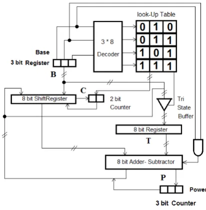
3 bit register named as Base (B) is used to store binary form of the Prime Base. Other 8 bit register named as Temporary (T) is used to store intermediate value.2 bit counter named as C is used to keep track of the number of shift operation are required for each power calculation and it is decremented by one for each Left shift operation is performed. Another 3 bit counter named as Power (P) is used to store binary form of (i-1) where i is the exponent. It is decremented by one for each power calculation. How many number of shift operations and either addition or subtraction operations are performed that are stored in look-up table for each Prime Base. First time according to the value of the Base one row of lookup table is selected by the decoder from B register value. 8 bit Adder Subtractor is used to perform addition and subtraction operation in same circuit only changing the input carry (0 for addition and 1 for subtraction). Finally Tri-state Buffer is used to keep the bus into high impedance state or active state using control input. Hardware circuit is given in Fig 2.
Fig. 2 Hardware Circuit
4.2. Hardware Circuit and Working Principle for Base 2
because tri state buffer is high impedance state .Then addition operation performed after that 3 bit counter decrement by one if it is equal to 0 then power calculation has completed and output of the adder-subtractor is the result, if not equals to 0 then output is loaded in shift register and 2 bit counter again loaded with ‘01’ again same operations are performed. This process will continue until the 3 bit counter value equal to 0 then output of the adder-subtractor circuit is the result.
4.3. Hardware Circuit and Working Principle for Base 3
According to the B register value (011), second row of the look up table is selected by decoder. LSB of B register is connected to control input of tri-state buffer .Input bus of the register T is kept in active state by the tri-sate buffer. Initially ‘011’ is contained by Shift Register and same binary value is copied into temporary register T. ‘01’ has been loaded by counter C from select row of look up table. The first and second MSB of B register have been used as inputs of AND gate. Output of the AND gate has been used as input carry of adder-subtractor circuit. So adder -adder-subtractor circuit is acting as adder here. After Left shift operation performed in by shift register counter value decrement by one. Temporary register counter contain 11 because tri-state buffer is in active state .Then addition operation performed after that 3 bit counter decrement by one if it is equal to 0 then power calculation has completed and output of the adder-sub tractor is the result, if not equal to 0 then output is loaded in shift register and 2 bit counter again loaded with ‘01’ again same operations are performed. This process will continue until the 3 bit counter value equal to 0 and then output of the adder subtract or circuit is the result.
4.4. Hardware Circuit and Working Principle for Base 5
According to the B register value (101), third row of the look up table is selected by decoder. LSB of B register is connected to control input of tri state buffer .Input bus of the register T is kept in active state by the tri sate buffer. Initially ‘101’ is contained by Shift Register and same binary value is copied into temporary register T. ‘10’ has been loaded by counter C from select row of look up table. The first and second MSB of B register have been used as inputs of AND gate. Output of the AND gate has been used as input carry of adder-subtractor circuit. So adder- subtractor circuit is acting as adder here. After Left shift operation performed in by shift register counter value decrement by one. Temporary register contain 101 because tri state buffer is in active state .Then addition operation performed after that 3 bit counter decrement by one if it is equal to 0 then power calculation has completed and output of the adder-subtract or is the result, if not equal to 0 then output is loaded in shift register and 2 bit counter again loaded with ‘10’ again same operations are performed. This process will continue until the 3 bit counter value equal to 0 then output of the adder subtractor circuit is the result.
4.5. Hardware Circuit and Working Principle for Base 7
According to the B register value (111), fourth row of the look up table is selected by decoder. LSB of B register is connected to control input of tri state buffer .Input bus of the register T is kept in active state by the tri sate buffer. Initially ‘111’ is contained by Shift Register and same binary value is copied into temporary register T.’11’ has been loaded by counter C from selected row of look up table. The first and second MSB of B register have been used as inputs of AND gate. Output (1) of the AND gate has been used as input carry of adder-subtractor circuit. So adder adder-subtractor circuit is acting as adder-subtractor here. After three Left shift operations are performed, shift register counter value is decremented by one. Temporary register contains 111 because tri state buffer is in active state .Then subtraction operation is performed after that 3 bit counter decrement by one if it is equal to 0 then power calculation has completed and output of the adder-subtractor is the result, if not equal to 0 then output is loaded in shift register and 2 bit counter again loaded with ‘11’ again same operations are performed. This process will continue until the 3 bit counter value equal to 0 then output of the adder sub tractor circuit is the result.
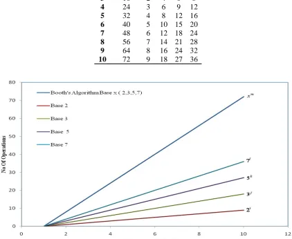
5. Performance Analysis
hand for booth’s algorithm the calculation involves the addition, subtraction, complements and shifts. So the computation overhead increases. The computation of 3j where j=2 the number of operations are 2; one shift and one addition, if j = 3 the number of operations are 4. But in the case of Booth’s multiplication method the computation of 32 requires 3 shifts, 2 subtractions, 1 addition and 2 complements a total of 8 operations. If j=3 then 16 operations are required in booth’s method. In power calculation of 2 one Logical Left Shift on ‘10’ increases the power by 2. If the given form is like 2i then total (i-1) no of Logical Left Shift operations are required. For base 3j , total (j-1) no of shift and addition operations are required. Finally for 5k and 7l, (k-1) no of two logical left shift followed by one addition and (l-1) no of 3 left shift operation followed by one subtraction operations are required respectively. The General procedure as in the case of Booth’s algorithm the number of operations is equal for each base unlike with the proposed method. The results for different values of xi j are given in the Table 1, where x (2,3,5,7) and (i,j,k,l 0,1,2,3,4,5…). A comparison has been given in Fig.3. Along the X axis, exponent (0, 1, 2, 3…) value and along Y axis, no of operation required to calculate each power of corresponding base have been drawn. For the Booth Algorithm method one line has been plotted because for each base required operations are same with different exponents but in case of proposed method four different straight lines have been plotted for different bases different exponents. Each line of the four is far away from the Booth’s algorithm line along the X axis that implies not only the individual base but also the overall performance is better in proposed approach.
Table 1. Performance Analysis
General Method
2
i3
j5
k7
l1 0 0 0 0 0
2 8 1 2 3 4
3 16 2 4 6 8
4 24 3 6 9 12
5 32 4 8 12 16
6 40 5 10 15 20
7 48 6 12 18 24
8 56 7 14 21 28
9 64 8 16 24 32
10 72 9 18 27 36
6. Conclusion
A simple shift and add or subtract technique has been introduced in this paper ,this method has great advantages over the general method. It explains that it needs less number of operations than Booth’s method for multiplication. Also a hardware circuit for calculation of exponent for different prime bases for multi base number system has proposed. VHDL simulation for this circuit has been opened as future work.
References
[1] Collin, Andrew. Andrew Booth’s Computers at Brikbeck College, Resurrection, Issue 5, Springer 1993. London: Computer Conservation Society.
[2] Vassil S Dimitrov, Graham A. Jullien, and William C. Miller, “ Theory and Application of the Double-Base Number system”, IEEE Transaction on Computers, Vol 48, No.10, Oct. 1999. Page-4.
[3] Subhashis Maitra and Amitabha Sinha. “A Single Digit Triple Base Number System - A New Concept for implementing High Performance Multiplier Unit for DSP Applications”.
[4] V. S. Dimitrov, G. A. Jullien, W.C. Miller, “An Algorit hm for modular exponentiation ”, Information Processing Letters(66)3 (1998) pp. 155-159.
[5] Soumen Debnath, Uddalak Mitra and Satrughna Singha, “ Exponential Power Calculation using Shift and Add Techniques”, National Conference on Recent Trends in Engineering and Technology including Non-Conventional Energy ( RTETNE-2010), pp. CSE & IT - 10, Jointly Organized by IMPS College of Engineering and Technology and The Institute of Engineering and Technology (U.K.), Kolkata Network, 10th April, 2010, Malda, West Bengal, India.
[6] Satrughna Singha and Amitabha Sinha, “Survey of Various Number Systems and Their Applications”, International Journal of Computer Science and Communication, Volume-1, Number-1, pp. 73-76, January 2010, Serials Publications, India.
[7] Sourav Samanta, and Maitreyee Dey, “Exponential Power Calculation of Single Digit Prime Number Using Hardware Circuit”, (ACADEMIC MEET 2011) , CS & IT-08, Abstract ,pp. 45-46 Organized by FOSET In Collaboration with WBUT, 12-13th March,
2011, Saltlake, Kolkata,West-bengal,India.
[8] Satrughna Singha, Supriya Chakraborty and Amitabha Sinha, “ Theory and Applications of the Double-Base Number System Using Bases 2 and 5”, International Journal of Computer Science and Communication, Volume-1, Number-1, pp. 97-100, January 2010, Serial Publications, India.