TORQUE RIPPLE REDUCTION IN VSI
FED INDUCTION MOTOR DRIVE
USING LOW SWITCHING FREQUENCY
G.Durgasukumar1, M.K.Pathak2
Electrical Engineering Department, I I T Roorkee India-247667
1[email protected], 2[email protected]
Abstract:
Multi-level voltage source inverters offer several advantages such as a better output voltage with reduced ripple, reduction of voltage ratings of the power semiconductor switching devices and also the reduced electro-magnetic interference problems etc. This paper presents torque ripple reduction for high power induction motors driven by five-level inverter with the low inverter switching frequency limited around 0.5–1kHz. It also presents an application of simplified space vector pulse width modulation (SVPWM) method for five-level fed inverters feeding a three-phase Induction motor and compares the torque ripple of induction motor drive fed with conventional two-level inverter and five-level inverter.
Keywords: Space vector modulation (SVM), Two-level inverter, Five-level inverter, Induction motor,
Torque ripple reduction.
1. Introduction:
In a conventional two-level inverter configuration, the harmonic reduction of an inverter output current is achieved mainly by raising the switching frequency. But in high power applications, the switching frequency of the power device has to be restricted below 1 KHz due to the increased switching losses and also the level of dc-bus voltage. On the other hand, the very high dv/dt generated with high dc-link voltage is responsible for the electromagnetic interference and motor winding stress [1]. So from the aspect of ripple reduction and high dc-link voltage level, multi-level inverters are more suitable.
Many researchers have worked on the space vector modulation of multilevel inverters [2-9]. In [2], a method of SVPWM for high level inverters that represents output vector in three-dimensional Euclidean space is presented. The method is based on the fact that increasing the number of levels by one always forms an additional hexagonal ring of equilateral triangles, which surrounds the outermost hexagon. In [3], the hexagon representing space vector diagram is flatten and the reference voltage vector is normalized in order to reduce computations of the algorithm. In [4], a SVPWM with a predictive current control loop have presented. In this load current is predicted for all output voltage vectors of the inverter. The current error is calculated and the switching state is selected when the value of the error is less. In [5], a space vector modulation allows reduction in the inverter output voltage distortion due to turn-off, turn-on and dead times of power modules, without increasing the harmonic content.
In [6], a simple space vector pulse width modulation algorithms for a multilevel inverter for operation in the over-modulation range have presented. In [7], a relationship between space-vector modulation and carrier-based width modulation for multilevel inverter has presented. In [8], a generalized method of space vector pulse-width modulation for multilevel inverter has presented. In this, instantaneous reference space vector position of a multilevel inverter is not required. Drawback of this method is it cannot identify the sector containing the reference space vector.
2. SVM for two-level inverter:
Fig.1 represents the two-level inverter and its space vector diagram with eight different switching states (V0-V7). No effective voltage is applied to machine when the zero vectors V0 and V7 are selected. The remaining six voltage vectors can be selected to apply an effective voltage to the machine and these vectors can be represented on the vector space with the stator fixed d-q reference frame. If a constant reference voltage vector Vref is given in one sampling period, this vector can be generated using zero vector (V0 or V7) in combination with only two nearest active vectors (V[n] and V[n+1]). These two active vectors are considered as the effective vectors to generate desired output voltage.
Fig.1. Two-level inverter and its Space vector diagram with active vectors
From the average voltage concept, the reference vector during one sampling period can be written as
Vref = (T1.Vn+ T2 .Vn+1)/Ts (1)
Where T1, T2 are the applied effective times corresponding to the active vectors V1-V6
The symbols T1 and T2 respectively denote that time periods for which the active vector along the lagging edge and leading edge that are switched for the realization of the reference voltage space vector in a given sampling time period. If the sampling time period of reference vector (Vref) is Ts, then the time periods T1 and T2 can be determined by equating the volt-seconds along the d and the q axes respectively.
Equating the volt-seconds along the d-axis
V cosα. T V . T V . cosπ . T (2) Equating the volt-seconds along the q axis
V sinα. T V . sinπ . T (3)
Where α is the angle of Vref in a 60o sector with respect to the beginning of the sector, Vdc is the magnitude of each active vector (V1-V6).
The effective time can be calculated as by solving the above equations
T1= V .T V . ·
π α
π = m. T · π
α
π (4)
T2= V T
V ·
α
π = m. T · απ (5)
T0= Ts-T1-T2 (6)
Where T1 is the time of switching vector that lags Vref, T2 is the time of switching vector that leads Vref, T0 is the time corresponding to null vector, Ts is the sampling time (1/fs)
m is the modulation index which is equal to VV
switching loss of the power semiconductor devices in the inverter, the switching should be in such a way that there is only one state transition.
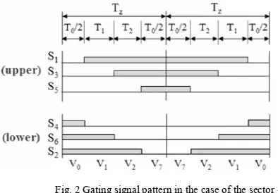
Fig. 2 Gating signal pattern in the case of the sector -1
Therefore, the actual switching times corresponding to the case of sector-1 can be written as
OFF Gating Sequence: ON gating Sequence: Tga=T0/2 Tga= T0/2+T1+T2 Tgb=T0/2+T2 Tgb=T0/2+T2 Tgc=T0/2+T1+T2 Tgc=T0/2
3. Simplified SVM for five level inverter:
3.1. Basic principle:
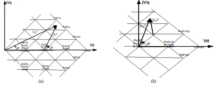
Fig 3 represents five-level inverter circuit diagram and its space vector diagram. Each leg is composed of four upper and lower switches with anti parallel diodes. The space-vector diagram of any multi-level inverter is composed of six hexagons, which can be reduced insteps further into the space-vector diagrams of conventional two-level inverters. The space vector diagram five-level inverter and its two level hexagons are shown in Fig.4. A five-level space-vector plane is transformed to the two-level space-vector plane by using the two steps.
[1] From the location of a given reference voltage, one hexagon has to be selected.
[2] The original reference voltage vector has to be subtracted by the amount of the center voltage vector of the selected hexagon.
Determination of switching sequence and the calculation of the voltage vector duration time is done as in conventional two-level SVPWM method.
Vdc Vdc Vdc Vdc v u w S1U S2U S1V S2V S1W S2W S3U S4U S5U S6U S7U S8U S3V S4V S5V S6V S7V S8V S3W S4W S5W S6W S7W S8W jVq Vd Vref
N2P2N N1P2N2 OP2N2 P1P2N2 P2P2N2
P2P1N P2P2N1 P1P1N1 P1P2N2 OP1N2 OP2N1 N1P1N N1P2N N2P1N N2P2N
N2P2O NN12PP11ON OP2O N1P1N N2ON2
P1P2O OP2N1 N1ON2
P2P2O P1P1N1 OON2
P2P1N1 P1ON2 P2ON2
N2P2P1 N1P2P1 N2P1O
OP2P1 N1P1O N2ON1
P1P2P1 OP1O N1ON1 N2N1N2
P2P2P1 P1P1O OON1 N1N1N2
P2P1O P1ON1 ON1N2
P2ON1 P1N1N P2N1N2
N2P2P2 N1P2P2 N2P1P1
OP2P2 N1P1P1 N2OO
P1P2P2 OP1P1 N1OO N2N1N1
P2P2P2 P1P1P1 OOO N1N1N1 N2N2N2
P2P1P1 P1OO ON1N1 N1N2N2
P2OO P1N1N ON2N2
P2N1N P1N2N
P2N2N
N2P1P2 N1P1P2 N2OP1
OP1P2 N1OP1 N2N1O
P1P1P2 OOP1 N1N1O N2N2N1
P2P1P2 P1OP1 ON1O N1N2N1
P2OP1 P1N1O ON2N1
P2N1O P1N2N P2P2N
N2OP2 N1OP2 N2N1P
OOP2 ON1P1 N2N2O
P1OP2 ON1P1 ON2O
P2OP2 P1N1P1 ON2O
P2N1P1 P1N2O P2N2O
N2N1P2 N1N1P2 N2N2P1
ON1P2 N1N2P2
P1N1P2 ON2P1 P
2N1P2 P1N2P1 P2N2P1
N2N2P2 N1N2P2 ON2P2 P1N2P2 P2N2P2
(a) (b)
Fig 4. Decomposition of five-level inverter into six two-level hexagons
3.2. Correction of reference voltage vector:
By the location of a reference voltage vector, one hexagon is selected among the six small hexagons that comprise the five-level space-vector diagram. The reference voltage vector should lie in the inner of the selected hexagon. This procedure divides the five-level space-vector diagram into six regions that are covered by each small hexagon. If the reference voltage vector stays in the regions that are overlapped by adjacent small hexagons, the multi-level space-vector diagram can have multiple values that are possible. Hexagon is identified by the number of S.
1 if
2 if 3 if S = 4 if
5 if 6 if
Where θ denotes angular position of reference voltage vector (V*) as represented in Fig 1 (b)
After selecting one hexagon the reference vector is transferred towards the center of the hexagon. Fig 5(a) and 5(b) represents first and second transformations of five-level. The transformation is done by subtracting the center of the selected hexagon from the original reference vector. Once the value is determined, the origin of a reference voltage vector is changed to the center voltage vector of the selected hexagon. This is done by subtracting the center vector of the selected hexagon from the original reference vector. Table I gives the d and q components of the reference voltage V3* for all six hexagons after first transformation.
(a) (b)
Fig.5 First and second transformations of original reference voltage vector in five-level
TABLE I TABLE II
d and q components of the reference voltage V3* d and q components of the reference voltage V2*
S V3*d V3*q
1 V5*d -2V.cos(0) V5*d -2V.sin(0) 2 V5*d -2V.cos(π/3) V5*d -2V.sin(π/3) 3 V5*d -2V.cos(2π/3) V5*d -2V.sin(2π/) 4 V5*d -2V.cos(π) V5*d -2V.sin(π) 5 V5*d -2V.cos(4π/3) V5*d -2V.sin(4π/3) 6 V5*d -2V.cos(5π/3) V5*d -2V.sin(5π/3)
TABLE III FIVE-LEVEL SWITCHING STATES
Switch ing Table
Switching states Term
-inal voltage S1u S2u S3u S4u S5u S6u S7u S8u
P2 on on on on off off off off 2Vdc
P1 off on on on on off off off Vdc
0 off off on on on on off off 0
N1 off off off on on on on off -Vdc
N2 off off off off on on on on -2Vdc
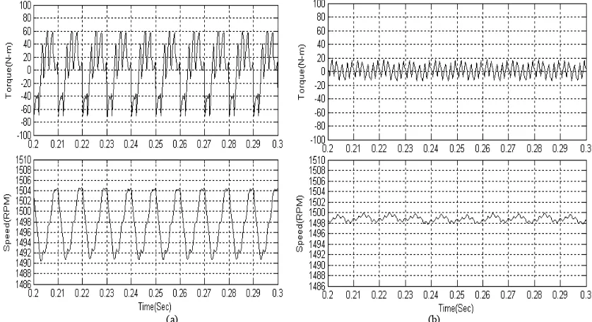
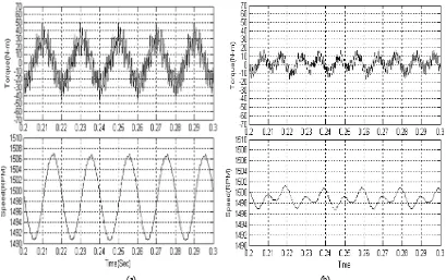
4. Results and Discussion:
The performance of induction motor drive fed from two-level and five-level are obtained under different inverter switching frequencies. The simulation results of two level inverter and five level inverter controlled drives under steady state are compared in Fig 6 and Fig 7 considering the sampling frequency fs=0.5 kHz and 1 KHz in SVM. When the switching frequency is 0.5 KHz, the torque ripple obtained with two-level inverter is varying between +60 to -60 where as with five-level inverter it is varying between +20 to -20. Similarly when the switching frequency is 1 KHz, torque ripple is varying between +50 to -50 with two-level, but it is varying between +15 to -15 with five-level. Due to this smooth speed response is obtained with five-level inverter compared to two-level inverter. From the simulation results, it is observed that the proposed five level inverter drive gives better results by reducing the ripple content compared to two-level inverter.
(a) (b)
Fig. 6 Torque ripple and speed oscillations under steady state at 0.5KHz with (a) two level (b) five level
S V2*d V
(a) (b)
Fig. 7 Torque ripple and speed oscillations under steady state at 1KHz with (a) two level (b) five level
5. Conclusion
A comparative study on torque ripple of two-level and five-level three-phase diode clamped inverters has been presented in this paper using simplified space vector modulation technique. It has been observed that with five-level inverter there is lot of improvement in the performance of induction motor compared to the conventional two-level inverter. The torque ripple significantly reduced by 65%, when the switching frequency is 0.5 KHz and 70% when the switching frequency is 1KHz with five-level inverter compared to two-level inverter. Due to the reduction in torque ripple the oscillation in speed response is less with five-level inverter.
References:
[1] X. Wu, Y. Liu, and L. Huang, “A Novel space vector modulation algorithm for three-level PWM voltage source inverter,” in Proc. IEEE Conf. Computers, Communications, Control and Power Engineering, Vol. 3, pp. 1974–1977, Oct. 2002.
[2] N. Celanovic and D. Boroyevich, “A fast space-vector modulation algorithm for multilevel three-phase converters,” IEEE Trans. Ind. Appl., vol.37, pp.637-641, 2001.
[3] M.M. Prats, R. Portillo, J.M. Carrasco, and L.G. Franquelo, “New fast space-vector modulation for multilevel converters based on geometrical considerations,” in Proc. 28th Annual Conf. Industrial Electronics Society, Vol. 4, pp. 3134–3138, Nov. 2002.
[4] G.S. Perantzakis, F.H. Xepapas and S.N. Manias, “ Efficient predictive current control technique for multilevel voltage source inverters,” in Proc. 11th EPE European Conf. Power Electronics and Applications, Dresden, 2005.
[5] C.Attainese, V.Nardi, and G.Tomasso, “Space vector modulation algorithm for power losses and THD reduction in VSI based drives,” Electrical power components and systems, vol.35, pp.1271-1283, 2007.
[6] Amit Kumar Gupta and Ashwin M. Khambadkone,” A General Space Vector PWM Algorithm for Multilevel Inverters, Including Operation in Over-modulation Range,” IEEE Trans. power. Electron., vol. 22, pp.517-526, March 2007.
[7] Wenxi Yao, Haibing Hu, and Zhengyu Lu, “ Comparisons of space-vector modulation and carrier-based modulation of multilevel inverter,” IEEE Trans. Power. Electron., vol. 23, pp.45-51, Jan.2008.
[8] Aneesh Mohamed, A.S.Anish Gopinath, and M.R.Baiju, “A simple space vector pwm generation scheme for any general n-level inverter,” IEEE Trans. Ind. Electron., vol. 56, pp.1649-1656, May 2009.
[9] Jae Hyeong Seo, Chang Ho Choi, and Dong Seok Hyun, “A new simplified space–vector pwm method for three-level inverters,” IEEE Trans. Power. Electron., vol. 16, pp.545-550, july 2001.
Appendix:
Three-phase, 400 V, 20 hp, 1500 rpm induction motor Parameters :
Rotor inductance Lr=0.065181 H, Rotor resistance Rr = 0.2205 Ω, Mutual inductance Lm=0.064191 H, Moment of inertia J=0.102 Kg-m2.
G.Durgasukumar received Bachelor’s and Master’s degrees in Electrical Engineering from
J.N.T.U, Hyderabad (India) and pursuing his Ph.D.degree in the Electrical Engineering Dept, Indian Institute of Technology, Roorkee, India. His research interests include power electronics and electric drives, machines.
Mukesh Kumar Pathak was born in Hamirpur (HP), India, in 1966. He did his graduation in