http://www.sciencepublishinggroup.com/j/ajesa doi: 10.11648/j.ajesa.20190702.11
ISSN: 2376-6069 (Print); ISSN: 2376-6085 (Online)
Dynamics of Data Conversion Schemes in High
Performance Voltage Circuit Systems Designs
Mohammed Babatunde Ibrahim
1, Kazeem Alagbe Gbolagade
1, Abraham Ayegba Alfa
21Computer Science Department, Kwara State University, Malete, Nigeria 2
Computer Science Department, Kogi State College of Education, Ankpa, Nigeria
Email address:
To cite this article:
Mohammed Babatunde Ibrahim, Kazeem Alagbe Gbolagade, Abraham Ayegba Alfa. Dynamics of Data Conversion Schemes in High Performance Voltage Circuit Systems Designs. American Journal of Embedded Systems and Applications. Vol. 7, No. 2, 2019, pp. 41-47. doi: 10.11648/j.ajesa.20190702.11
Received: July 11, 2019; Accepted: September 27, 2019; Published: October 10, 2019
Abstract:
Several efforts are being made in the field of voltage converters due to increasing focus in power electronics. This is hinged on simple fact that converters have widespread usability domain such as portable devices running on battery, PCs, industrial electronic equipment, telecoms systems, and stable power distribution. Currently, studies are focusing on developing highly effective converter systems and designs innovations that take advantage of limited energy resources to improve and increase power/voltage supply capabilities for electronic devices consumptions. Power supply mechanism is analogous to data conversion systems outcomes in which voltage is generated in circuit systems through series of conversions and reversions. This study proposes hybridization of two existing data conversion schemes in the design of highly effective voltage circuits system that can tolerate and improve energy consumptions issues. The result indicates that the hybrid voltage pin of 63V is higher than the circuits system of the single voltage source of the analog and direct voltage which generated 54V and 6V respectively. The hybrid voltage pin also outperformed another investigative paper by 63V to 32V for an input of 5V leading to the hybrid converter offering more gains for low voltage source by 66.7% (9V) to 33.3% (5V) respectively.Keywords:
Analog, Digital, Converters, High Performance, Voltage, Circuits Systems Design1. Introduction
Power converters are electronic circuits concerned with the conversion, regulation and conditioning of electric voltage supply. The power outputs range from milliwatts in mobile devices to megawatts in electric power transmission systems. Reliability is interestingly the main focus of many industrial power converters. Electronic devices and control circuit are expected to be highly robust in order to attain a high valuable life. The special focus given to the overall efficiency of power electronic circuits is due to inestimable environmental and economic value of wasted power and, cost of energy dissipated which it can generate. In effect, an insignificant improvement in converter power efficiency can translate to better returns of the investment in the electronics sector [1]. One major electronic converter is Switched-Mode Power Converters (SMPC).
The application of Residue Number System (RNS) in
2. Literature Review
2.1. Voltage Supply Challenges
The solar power, RF power, and fuel cells are most feasible alternatives of voltage supply [3]. But, the major challenge of these power sources is the low level of their voltage output levels. A single solar cell delivers approximately 0.5V, which is much lower than many alternative sources such nominal voltage of dry cells or even their end-to-discharge values of 0.9V. Integrated circuits (ICs) are being designed to improve the capability of solar cells and systems to deliver better solutions for portable signal processing instruments. ICs need much greater voltages to function properly, which make voltage multiplication desirable. The prospect of attaining enhanced DC voltage on-chip is achieved through voltage multiplication. This is a noisy and unsupportive of sensitive analog circuits due to power supply rejection of the later. Recently, the rising demands for designing and perfecting low circuits with low power consumption.
In practice, low power consumption of circuit operation involves low voltage. But, performance of circuit degrades and bandwidth. In many cases, these losses can be restored by scaling down the voltage threshold of MOSFETs, which increases static power dissipation. For analog circuits, scaling can be very efficient; and the use of minimum size transistors is unfit due to noise and offset voltage constraints. This is different with digital circuits which results in improved performances. Low voltage analog circuit design techniques differ considerably from those of high voltage analog circuit design. This generates a need for adaptation of alternative design techniques to suit the low voltage environments. The current mode approach proves a better alternative for low voltage high performance analog circuit design in which the focus is on current levels for the operation of the circuits. The voltage levels present at various nodes are immaterial.
Analog signal processing has undergone several developments especially in real time application which are analog by nature for physical phenomenon. Also, there is an increased market demand for complex and advanced information processing applications which is fuelling more focus on analog system design. In recent times, VLSI is an offshot of analog design which has traversed to the digital VLSI design with VLSI technology and CAD tools. At present, analog cells are similar to digital system design, which implies analog systems can be built as though digital system. Therefore, the design became simpler such as Field programmable analog arrays, configurable and modular analog circuits [4, 5]. In general, electrical circuits can be created from the interplay between current and voltage. Majority of conventional analog circuits such as operational amplifiers and voltage mode circuits, but, the output of the voltage is sluggish due to stray and capacitances in the event of increases in input voltage. Again, the voltage mode circuits have low bandwidth with high slew rate which make it unfit for high frequency applications having high voltage savings [6]. The voltage signals are unconnected to the
circuit performance. Analog circuits are expected to exhibit rail-to-rail input and output voltage swing capability. Several conventional circuit topologies have been overtaken by fresh innovative design. Simple Current Mode Circuit structures, especially those circuits that are capable of operating at low voltages have been developed [7].
2.2. Application of Residue Number Systems
Residue Number System is a mathematical concept discovered by Sun Tsu Suan-Ching in 4th century AD from original operations of Chinese remainder theorem of modular arithmetic. In 1950s, the focus on RNS arithmetic increased because of support for computational hardware and diverse applications such as digital filtering, coding, RSA ciphering system, digital communications, digital signal processing and storing and retrieving information, error detection and correction and fault tolerant systems [8]. In particular, RNS are characterized by modularity, fault tolerance, parallelism and carry free functions. Recently, RNS-based architectures have been implemented because of benefits of VLSI technology. Consequently, many high-speed and special purposes VLSI digital signal processor have effectively developed. Another advantage of RNS is the capability of representing a large integer with a collection of smaller integers. The component of RNS model include: forward conversion, channels (moduli) and reverse conversion as shown in Figure 1.
Figure 1. Structural components of RNS model. [9].
2.3. Forward Conversion
Figure 2. RNS based forward conversion. [9].
One way of implementing a residue adder for modulo ‘m’ structure is composed of one n-bit adder among various ways [10].
2.4. Channels
The Standard channels in RNS are three moduli such as 2 1, 2 , 2 1 in which n depicts the way of splitting the decimal value (X) considered in Figure 1. During the design of RNS system, it is important to choose appropriate moduli set because of the influence on the complexity of Forward and Reverse converters, and RNS arithmetic Circuits. Unbalanced moduli-sets lead to uneven architectures, in which the operation of main moduli in terms of cost and performances is overly dominant [11].
2.5. Reverse Conversion
Reverse conversion is the act of converting residue number to binary number by means of conversion algorithms such as Chinese Remainder Theorem (CRT), Mixed Radix Theorem
(MRT), and New Chinese Remainder Theorem (NCRT). The purpose of the NCRT is to speed up the computation in an efficient devoid of additional overheads. For the three moduli residue number system 2 1, 2 , 2 1 a new high-speed ROM-less residue-to-binary converter is utilised. Not like other converter, its delay consists of the time of only one 1's complement addition of two 2n-bit numbers which is about 2/3 of the binary range of the RNS equal to as 3n. Therefore, it is arguably the fastest available residue-to-binary converter [12].
2.6. High Voltage DC Transmission
High Voltage Direct Current (HVDC) transmission is beneficial for long distances and asynchronous interconnection of power delivery through underground cables and overhead lines. Conventionally, HVDC systems are faster, well-established technology, and controllably stable since inception in 1954 by Sweden. The classic HVDC transmission based on thyristors are deployed for power conversion from AC-to-DC and DC-to-AC [13]. Later, Voltage Source Converter (VSC) was introduced to replace thyristors, which is an advanced semi-conductor technology. The advantages of VSC-based HVDC over classic-based HVDC installation include independent control of active and reactive power, and distinct power systems interconnection. Recently, VSC HVDC is used to reverse the flow of power direction without changing the polarity of DC voltage (in multi-terminal DC system), which is needless of fast communication between the two converter stations [14].
The HVDC back-to-back converter is made up of a rectifier and an inverter interconnected with a shared DC link located in same site with connectionless bridges as shown in Figure 3. Usually, the DC link voltage must exceed the peak line operating voltage; and regulated by controlling the power flow to the AC grid. More importantly, there is capability to speedily control the power flow.
Figure 3. HVDC converter system. [15].
2.7. Types of Circuit System Designs
Similarly, the devices within converters can be switched in different ways [1]. When devices switch at the line frequency (50Hz or 60HZ) offers line frequency converters (naturally commutated converters) or high-frequency switching (forced-commutated converters). Whatever the character of the input source, converters can be classified as voltage-source converters or current-source converters. Also, converters can
be of low, medium or high voltage and/or current level. In addition, converters can be classified on basis of the size of the output signal obtained from the input signal; when the converter accomplishes a lower output signal it is referred as
step-down, and when it obtains a larger signal, it is referred as step-up [16].
2407A DSP to fire the pulses into the super-lift converter because of high processing speed, ADC units, PWM generation units and flexible instruction set. The outcome of the converter is supplied to processor by means of the ADC channels. The ADC converter is compared with established value to determine error generated. However, the voltage conversion scheme requires closed loop control for efficiency. The work is valuable because of power voltage enhancement and error correction design features for analog and digital signals considered.
The study [18] developed a structured residue number system based building blocks to improve the efficiency of digital processing applications. The author considers non-weighted number system for carry-free, parallel, high speed, secure and fault tolerant arithmetic operations for the purpose of constructing high-performance and fault tolerant digital signal processing (DSP) applications. Three parts of the DSP were proposed. Firstly, binary to residue converter which manipulates the RNS equivalent of the inputs represented in the binary number system. Secondly, parallel residue arithmetic units which compute arithmetic operations on the operands available in RNS represented. Thirdly, the residue to binary converter converts of outputs back into binary representation. The outcomes show that RNS- based image processing is more efficient in terms of timing performance and power consumptions when compared to binary-based structures.
The study [19] undertook the challenge of data conversion in RNS because of RNS prospects in hardware applications. Data conversion circuits in hardware remained a serious problem because of overhead involves in circuits designs. The author proposed an effective method for converting conventional representation to and from RNS, which are two including direct analog-to-residue conversion, residue-to-analog. In general, analog continuous-time signal and digital signal representation are forms of binary formats available. The performance of the two schemes showed the efficacy of RNS in applications requiring analog interactions and communications. The short fall of this work is lesser adoption of RNS in hardware and circuit designs as compared to binary formats.
The study [20] applied residual arithmetic in communication and signal processing in which the arithmetic operations are split into smaller parallel independent operations without a carry propagation. The moduli set is selected without carry generation. The author used residue number system (RNS) in designing solution to various applications of Communication and Signal Processing especially in applications where integer arithmetic is authoritative process.
The study [21] proposed the use of Residual Number System (RNS) to overcome the limitation posed by the 2’s complement number system in power-performance efficiency due to its sequential carry propagation. The author introduces the concept of parallel independent operation partitioning, which produce faster and power-efficient hardware. This study is limited to hardware application domain with less advantageous in a programmable processor especially the
overheads incurred in the conversion operations for transforming operands from 2’s complement to RNS and vice-versa. The results showed that application performance improved by 21% and an average functional-unit power improvement by 54%.
3. Methodology
This paper proposes a three step process approach for converting low voltage input to a different frequency signal, whose output is a higher voltage variant. This is achieved by taking advantage of conversion schemes in order to produce high frequency signals circuit system. In general, the electrical circuit system controls and modifies the low power sources or inputs by means of signal converters with the goal of attaining high-voltage efficiency. Again, the converters vary the voltage supply in the system block Chips (SoCs) on the basis of power efficiency and required performance as illustrated in Figure 4.
Figure 4. Structure of the proposed voltage circuit system design.
In Figure 4, the voltage sources or inputs are composed of direct current (DC), alternate current (AC) and noise variables. These components are combined in circuit design to produce resultant voltage supply from the source unit which is transmitted across positive and negative terminals is given by Equation 1.
= sin 2 + + 1
where,
is the hybrid voltage source
is steady-state DC voltage component is the amplitude of the AC voltage component is the frequency of the AC component
is the time of the AC component
is the phase offset of the AC component, and is the noise voltage
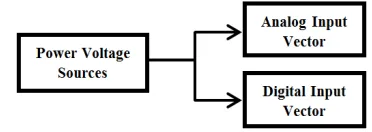
The first step of the proposed electrical circuit design is to execute the conversion scheme which separates voltage sources to their corresponding analog and digital vectors signals as illustrated in Figure 5.
Figure 5. Hybrid voltage source conversion structure.
in the resulting output vector. The block interconnects each volt value generated from the hybrid power source to a set of M bits, using the selection for the output bit order selection to ascertain the most significant bit, which gives resulting vector length M
times the length of power voltage source (or input) vector. The number of bits per voltage supply parameter is M. The unsigned values of input vectors are constrained to 0 and 2M – 1. In the case of signed input variable, the values are restricted to –2M – 1 and 2M – 1 – 1. At run-time, checks and fault detection are carried out whenever the input values surpass this specified range. This process is effective as single-rate and single-channel that operates length, N column vector (or a scalar-value: N = 1) input signal with matching outputs of length N·M column vector. The second step converts every analog input vector to digital input vector before generating binary signals using analog-to-digital converters such as C281xADC algorithm that uniquely create binarized input pins as shown in Figure 6.
Figure 6. Binary input pins generation for the voltage signals.
From Figure 6, the voltage signals can be effectively converted into binary form for analog and digital vectors signals respectively.
The third step is a hybrid conversion scheme which generates RNS representations for binary input pins realized from second step. This reduces noise and errors inherent in these signals in order to improve the resultant voltage output in circuit system for the different power sources (that is, analog and digital binary input pins) as illustrated in Figure 7.
Figure 7. The RNS based circuit systems design.
The proposed circuit system design makes use of Reed-Solomon (RS) converter, which is RNS dependent. The RS converter transforms the binary digital signal of length K and codeword length (N – number of punctures) to residue input pin. The binary sequences of length M is mapped to elements of the three moduli residue number system [0, 2 , 2 − 1], where the first bit in each sequence is the most significant bit (MSB) for non-negative integer (M). Thereafter, the Hamming code converter is introduced to generate the final transformation of binary analog signals component of the voltage source to residue. This converter creates residue signal with message length K and codeword length N. the number N has the form 2M – 1, where M is an integer greater than or equal to 3, and K = N – M. The binary analog signal to converter with vector size of K creates corresponding residue signal vector outcome size N. The implementation is achieved by means of MATLAB R2010a.
4. Results
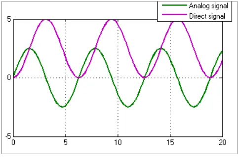
The difference between the analog and direct voltage signal signals derived from power source are illustrated in Figure 8.
Figure 8. Analog vs. direct voltage signals.
From Figure 8, the values of the analog and direct voltage signals realised from the sources are presented in Table 1.
Table 1. The values of voltage signals sources compared.
Time (sec) 0 0.4 0.8 1.2 1.6 2 2.4 2.8 3.2 3.6 4 4.4 … 20.0 Volts
Signal 1 0.0 0.2 0.4 0.6 0.7 0.8 0.9 1.0 1.0 1.0 0.9 0.8 … -0.5 8.9
Signal 2 0.0 0.0 0.1 0.2 0.3 0.5 0.6 0.8 1.0 1.2 1.4 1.6 … 1.8 53.6
In Table 1, the signal 1 and signal 2 are the voltage (9V and 54V) delivered from the analog and direct power sources after 20 sec of simulation respectively. The analog voltage is less effective to direct voltage delivered independently. The hybrid converter combines these two voltage sources in order to enhance the power supplied in power circuits. The binarization process is built into voltage circuit system to
take advantage of these distinct voltage sources to provide higher voltage signals for the power circuit system. This is achieved by first converting analog-to-direct voltage signal. Then, the resulting direct signals are converted into 16 binary pins using Bit-to-Residue number system converter as illustrated in Table 2.
Table 2. Voltage pins generation.
Signal 1 pin 0 0 0 0 0 0 0 0 0 0 0 0 1 0 0 1
The hybrid model combines the signal 1 and signals 2 pins to produce high voltage which is more than each voltage source selected separately as presented in Table 3.
Table 3. Hybrid voltage source generated.
Signal 1 pin 0 0 0 0 0 0 0 0 0 0 0 0 1 0 0 1
Signal 2 pin 0 0 0 0 0 0 0 0 0 0 1 1 0 1 1 0
Hybrid pin 0 0 0 0 0 0 0 0 0 0 1 1 1 1 1 1
The voltage value of hybrid pin is 63V, which is higher than circuits system running on single voltage source design. In this case, analog and direct voltage sources generated 54V and 9V respectively lower than the hybrid voltage source design for a power circuit system. In a work by the study [17], output of 32V is produced for an input of 5V, which implies the hybrid converter offered more gains for low voltage source by 66.7% (9V) to 33.3% (5V) respectively.
5. Conclusion
Power converters control the flow of power between two circuits systems by changing the character of electrical energy including: from direct current to alternating current, from one voltage level to another voltage, or in other way. One common classification of power conversion systems is associated with the waveform of the input and output signals, which is Alternating Current (AC) or Direct Current (DC) [22]. These popular power converters include: DC to DC, DC to AC Inverter, AC to DC Rectifier, and AC to AC Transformer. This paper has established that hybrid power source designs based on residue number system are more effective for high performance circuits systems. However, there are possible prospects of deploying Residue Number System based converters to improve output of electrical circuits systems.
References
[1] J. G. Kassakain and M. F. Schlecht, High-frequency high-density converters for distributed power supply systems. Proceedings of the IEEE, vol. 76, no. 4, pp. 362-376, 1998. [2] A. C. Sanchez, Control design for electronic power converters.
Unpublished Ph.D. thesis, Department of Engineering Science and Automatic, University of Sevilla, Spain, 2010.
[3] L. Benini, G. D. Micheli, and E. Macii, Designing Low Power Circuits: Practical Recipes, IEEE Circuits and Systems Magazine, vol. 1, no. 1, pp. 6–2, August 2001.
[4] S. R. Zarabadi, F. Larsen, and M. Ismail, A Configurable Op Amp/DDA CMOS Amplifier Architecture, IEEE Transactions on Circuits and Systems—I, vol. 39, no. 6, pp. 484–487, June 1992.
[5] M. Ismail and S. Bibyk, CAD Latches onto New Techniques for Analog ICs, IEEE Circuits and Devices Magazine, pp. 11– 17, September 1991.
[6] M. Ismail and T. Fiez, Analog VLSI Signal and Information Processing. NewYork: McGraw-Hill, 1994.
[7] S. Yan and E. Sanchez-Sinencio, Low Voltage Analog Circuit
Design Techniques: A Tutorial, IEICE Transactions on Fundamentals, vol. E83–A, February 2000.
[8] S. Piestrak, A high speed realization of a residue to binary number system Converter, IEEE Transactions on Circuits and systems-II, vol. 42, no. 10, October 1995.
[9] N. Vivek and K. Amusudha, Design of RNS Based Addition Substraction and Multiplication Units, International Journal of Engineering Trends and Technology, vol. 10, no. 12, pp. 593-596, April 2014.
[10] A. P. Vinod and A. B. Premkumar, A memoryless reverse converter for the 4-moduli superset {2n-1, 2n, 2n + 1, 2 n+1-1}, Journal of Circuits, Systems, Computers, vol. 10, no. 1&2, pp. 85–99, 2000.
[11] Somayyeh Jafarali Jassbi, Keivan Navi, and Ahmad khademzadeh, An Optimum Moduli Set in Residue Number System, International Journal of Mathematical Forum, vol. 5, pp. 2911-2918, March 2010.
[12] P. Samundiswary and S. Kalpana, Design and Analysis of RNS based FIR Filter using Verilog Language, International Journal of Computational Engineering and Management, vol. 16, issue 6, November 2013.
[13] S. Cole, et al., Technical developments for the future transmission grid, International Conference on Future Power Systems, 2005, pp. 6.
[14] J. P. C. Roberto Rudervall, Raghuveer Sharma, High Voltage Direct Current (HVDC) Transmission Systems Technology Review Paper, Sweden, Unated Stated.
[15] S. Meier, Novel Voltage Source Converter based HVDC Transmission System for Offshore Wind Farms, Department of Electrical Engineering Electrical Machines and Power Electronics, Royal Institute of Technology, Stockholm, 2005.
[16] E. Acha, Switching Power supply design. New York: McGraw Hill 1997.
[17] V. Balaji, and N. C. Eshwar, Implementation of a positive output Superlift converter. Unpublished B. Eng Thesis, Anna University, Department of Electrical & Electronics Engineering, Chennai 2006.
[18] D. Younes, Residue Number System Based Building Blocks for Applications in Digital Signal Processing. Unpulished
Ph.D. thesis, Bruno University of Technology, Brno, Czech Republic, 2013.
[19] O. Abdelfattah, Data conversion in residue number system. Unpublished M. Eng Thesis, McGill University, Montreal, Canada, 2011.
[21] R. G. Choski, Residue Number System Enhancements for Programmable Processors. Unpublished MSc Thesis, Arizona State University, Arizona, USA 2008.
![Figure 1. Structural components of RNS model. [9].](https://thumb-us.123doks.com/thumbv2/123dok_us/985681.1598204/2.595.309.544.414.552/figure-structural-components-of-rns-model.webp)
![Figure 2. RNS based forward conversion. [9].](https://thumb-us.123doks.com/thumbv2/123dok_us/985681.1598204/3.595.50.285.75.252/figure-rns-based-forward-conversion.webp)