205 | P a g e
ANALYSIS AND SIMULATION OF Z SOURCE
INVERTYER USING PM SYNCHRONOUS MOTOR
DRIVE
B Ashok Kumar
1, Dr. P Ram Kishore Kumar Reddy
21,2
Department of Electrical and Electronics Engineering,
Mahatma Gandhi Institute of Technology, Hyderabad, (India)
ABSTRACT
In the PM Synchronous Motor (PMSM) the excitation is provided owing to permanent magnet instead of the field windings. Special construction causes that the PMSM Motor has sinusoidal back EMF. The motor requires sinusoidal stator currents to produce constant torque. PMSM is simple in construction due to its robustness PMSM used in the many industrial application and control to Adjustable Speed Drives. In this paper analysis of the z source inverter using PMSM is proposed. The z source network is a DC link Energy storage sub circuit was proposed in the paper z source network is used for AC-DC /DC-AC power conversion circuit due its advantages compare to the traditional LC, DC links. In the paper analysis of z source inverter and operating principle of the ZSI and the advantage of ZSI using the Adjustable Speed Drives is proposed. The proposed system topologies are validated by using the MATLAB/SIMULATION ,SIMULINK environment.
Keywords:
PM Synchronous Motor Drives, Z Source Inverter, Inverter TopologyI.INTRODUCTION
For the environmental protection and energy saving, Fuel cell, photovoltaic cell and super capacitor can be
employed to supply electric energy in the Electric vehicle, due to their environmental friendly nature the PMSM
offers a potential candidate for used in the electric drive applications, where the portability and efficiency
required. Especially Fuel cell is regarded as the future clean energy source. It is well known that the output
voltage of fuel cell is decrease with increase in the output current. To overcome this problem, at present there
are two main solutions are present, the traditional dc-dc boosted PWM Inverter and the original Z Source
inverter proposed in the reference[1]
206 | P a g e
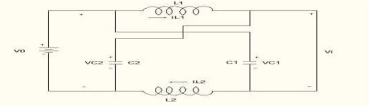
Fig. 1 Equivalent circuit of Z source inverter
One of the major problem the voltage source inverters, having in the input stage batteries, photovoltaic systems,
and fuel cells or a diode rectifier fed by the 230 V ac line, is the DC link voltage level, which could be smaller
than the desired level, imposed by applications. The VSI are used in photovoltaic systems as well as inverter
based motor drives system. A growing interest also shown in the field of electric vehicles. The main reason why
the Z-Source Inverter network seems to be god choice for the intermediate connection between the DC link
voltage and inverter are the following, it provides greater voltage than the desired voltage level if it is necessary,
it makes inverter immune to short circuits produced by the conduction of both transistor on the same phase leg,
it reduce the inrush current and harmonics in the current this can be done by the inductors in the Z-Source
network, and it forms a second order filter and handle the undesirable voltage sags of the DC voltage
source[1-7]
Fig. 2 presents the electric circuit of the Z-Source Network connected to a Three phase inverter, the diode D at
the front end of the Z Source network makes circuit unidirectional. The electrical energy flows from the DC
voltage source to Load.
Fig 2: Z source network connected to Three phase Inverter
Compare with the former, the Z source inverter has more advantages such has higher efficiency and lower cost,
which is very promising for FC systems due to its novel voltage buck/boost ability [2]. The interrelated
literatures [1-6] demonstrated the unique features of Z source network and its feasibility for the adjustable speed
drives (ASD) systems with induction machines.
PMSM Drives fed by the Z source inverter may have the advantages of both of them, and be suitable for the FC
based electric drive systems. This paper investigates the PMSM drive system fed by Z source inverter. Firstly,
207 | P a g e
space method is used for mathematical modeling. Finally, simulation results are carried out to verify the desiredperformance of the proposed system
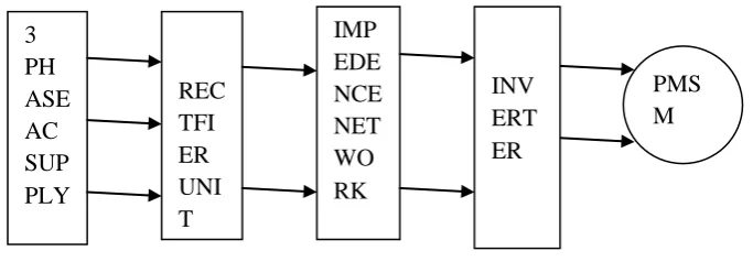
Fig 3 represents the Block Diagram of PMSM drive system.
From the below Block Diagram explained as when ever given the AC Supply to the system it will be converted
to DC using the rectifier unit which present in the system and then the next block is the impedance source
network the output of the rectifier is given to the Z source network and then the output of the Z source network
will be given to the inverter by using inverter convert DC-AC and the output of the inverter will be given to the
Load
Fig 3 Block Diagram of the Z source inverter
II. EXISTING SYSTEM
Inverters are the dc to ac converters. The input dc supply is either in the form of voltage or current is
converted in to variable output ac voltage. The output ac voltage can be controlled by varying input dc
supplier by varying the gain of the inverter. There are two types of traditional inverters based on input source
used in industries for variable speed drive and many other applications; those are
A) voltage-source inverter
B) current-source inverter
Inverter in traditional voltage source inverter (vsi), the dc voltage source connected at the input
capacitor. Dc link voltage produced across this capacitor feeds the main bridge. The input dc supply can be
a battery or fuel cell stack or diode rectifier, and/or capacitor. The bridge inverter circuit consists of four
switches; each is composed of a power transistor and an anti- parallel diode to provide bidirectional current flow
and reverse voltage blocking capability. In traditional current reversible voltage blocking capability. in
traditional voltage source inverter (csi), the dc current source is formed by a large dc inductor fed by a voltage
source such as a battery or fuel-cell stack or diode rectifier or converter etc. Like Vsi Bridge inverter circuit
consists of four switches; each is composed of a switching device with reverse block capability such as a
thyristor and scr or a power transistor with a series diode to provide unidirectional current flow and bidirectional
208 | P a g e
voltage blocking. For voltage source Inverter and current source inverter the on/off time the switching devices iscontrolled by applying control voltage (PWM) to the control terminal i.e. Gate of the device.
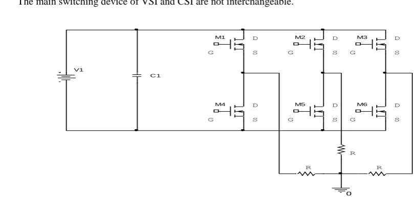
Fig 4 represent the circuit diagram of Existing system Voltage Source Inverter
The operation of the traditional voltage source inverter is like normal three phase voltage source inverter. It will
be conduct in 1200 and 1800 in the 1200 conduction at a time 2 switches will be conduct where vas in 1800
conduction at a time 3 switches will be on, whenever the two switches will be on in the same leg it will be
causes a short circuit in the system, this is the disadvantage of the traditional Voltage Source Inverter. Some of
the disadvantages of traditional VSI can be given below
Typical inverters (VSI and CSI) have few disadvantages. They are listed as,
Behave in a boost or buck operation only. Thus the obtainable output voltage range is limited, either
smaller or greater than the input voltage.
Vulnerable to EMI noise and the devices gets damaged in either open or short circuit conditions. The combined system of DC-DC boost converter and the inverter has lower reliability.
The main switching device of VSI and CSI are not interchangeable.
0
V1
C1
M1 M2 M3
M4 M5 M6
D D
D
D D D
S
S S S
S
G G G
G G
G S
R
R R
Fig 4: Traditional Voltage source Inverter
To overcome these disadvantages a new concept was developed in year 2002 by Dr. F.Z. Peng. This involves
combination of VSI and CSI to form a cross coupled network of two inductors and two capacitors, known as
Impedance Network..
III. OPERATING PRINCIPLE AND MATHEMATICAL MODELING OF PROPOSED
SYSTEM
209 | P a g e
The Z-source inverter is a buck–boost inverter that has a wide range of obtainable not (vectors) unlike thetraditional inverter bridge that has six switching states. When the load terminals are shorted through both the
upper and lower devices of any one phase leg (i.e., both devices are gated on) or two phase legs shoot through
zero state occurs. This shoot-through zero state (or vector) is forbidden in the traditional V-source inverter,
because it would cause a shoot-through. The Z-source network makes the shoot through shoot-through zero state
possible. This shoot-through zero state provides the unique buck-boost feature to the inverter. The
inverter bridge is equivalent to a short circuit when the inverter bridge is in the shoot through zero states, where
as the Inverter bridge becomes an equivalent current source where in one of four active states. These shoots
through states are provided by simple boost controlled PWM technique.
Normally, three phase inverters have 8 vector states (6 active states and 2 zero states). But ZSI along with these
8 normal vectors has an additional state known as the shoot through state, during which the switches of one leg
are short circuited. In this state, energy is stored in the impedance network and when the inverter is in its active
state, the stored energy is transferred to the load, thus providing boost operation. Whereas, this shoot through
state is prohibited in VSI.
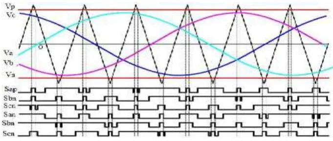
To achieve the buck-boost facility in ZSI, required PWM is as shown in figure. The normal Sinusoidal PWM
(SPWM) is generated by comparing carrier triangular wave with reference sine wave. For shoot through pulses,
the carrier wave is compared with two complementary DC reference levels. These pulses are added in the
SPWM, highlighted in figure. ZSI has two control freedoms modulation index of the reference wave which is
the ratio of amplitude of reference wave to amplitude of carrier wave and shoot through duty ratio which can be
controlled by DC level.
The Z-source inverter is analyzed using voltage source inverter. The unique feature of the Z-source inverter is
that the output ac voltage can be any value between zero and infinity regardless of the input DC voltage. That
is, the Z-source inverter is a buck–boost inverter that has a wide range of obtainable voltage. The traditional V-
and I-source inverters cannot provide such feature.
The main feature of the Z-source is implemented by providing gate pulses including the shoot-through pulses.
Here how to insert this shoot- through state becomes the key point of the control methods. It is obvious that
during the shoot-through state, the output terminals of the inverter are shorted and the output voltage to the load
is zero. The output voltage of the shoot- through state is zero, which is the same as the traditional zero states,
therefore the duty ratio of the active states has to be maintained to output a sinusoidal voltage, which means
shoot-through only replaces some or all of the traditional zero states.
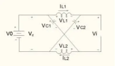
Let us briefly examine the Z-source inverter structure. In Fig. 3, the three-phase Z-source inverter bridge has
nine permissible switching states (vectors) unlike the traditional three-phase V-source inverter that has eight.
The traditional three-phase V-source inverter has six active vectors when the DC voltage is impressed across the
load and two zero vectors when the load terminals are shorted through either the lower or upper three devices,
respectively. However, three-phase Z-source inverter bridge has one extra zero state (or vector) when the load
terminals are shorted through both the upper and lower devices of any one phase leg (i.e., both devices are gated
on), any two phase legs, or all three phase legs. This shoot-through zero state (or vector) is forbidden in the
210 | P a g e
shoot-through zero state (or vector), which can be generated by seven different ways: shoot- through via any onephase leg, combinations of any two phase legs, and all three phase legs.
The Z-source network makes the shoot-through zero state possible. This shoot-through zero state provides the
unique buck-boost feature to the inverter. The Z-source inverter can be operated in three modes which are
explained in below.
(i)Mode I:
In this mode, the inverter bridge is operating in one of the six traditional active vectors; the equivalent circuit is
as shown in figure 5
Fig.5: Equivalent Circuit of the ZSI in one Fig. 6: Equivalent Circuit of the ZSI in one of
of the Six Active States the two traditional zero states
The inverter bridge acts as a current source viewed from the DC link. Both the inductors have an identical
current value because of the circuit symmetry. This unique feature widens the line current conducting intervals,
thus reducing harmonic current.
(ii)Mode II:
The equivalent circuit of the bridge in this mode is as shown in the fig. 6
The inverter bridge is operating in one of the two traditional zero vectors and shorting through either the
upper or lower three device, thus acting as an open circuit viewed from the Z-source circuit. Again, under
this mode, the inductor carry current, which contributes to the line current’s harmonic reduction as shown in
211 | P a g e
Fig 7: Equivalent Circuit of the ZSI in the Fig. 8: Equivalent Circuit of the ZSI in the
Non Shoot-Through States. Shoot through states
(iii)Mode III:
The inverter bridge is operating in one of the seven shoot-through states. The equivalent circuit of the inverter
bridge in this mode is as shown in the below figure 8. In this mode, separating the dc link from the ac line.
This shoot-through mode to be used in every switching cycle during the traditional zero vector period generated
by the PWM control. Depending on how much a voltage boost is needed, the shoot-through interval (T0) or its
duty cycle (T0/T) is determined. It can be seen that the shoot-through interval is only a fraction of the
switching cycle.
For simplicity, assuming that the inductors L1 and L2 and capacitors C1 and C2 have the same inductance
and capacitance respectively, the Z-source network become symmetrical.
3.2 Shoot Through PWM Control
There are several control methods such as: simple boost control, maximum boost control, and maximum
constant boost control[9].
In traditional PWM switching sequence based on the triangular carrier method. In every switching cycle, the
two non-shoot-through zero states are used along with two adjacent active states to synthesize the desired
voltage. When the dc voltage is high enough to generate the desired ac voltage, the traditional PWM is used.
The shoot-through period is generated by comparing the same triangular wave with straight lines or
envelopes of the modulating signal or sinusoidal signal depending upon the technique used and inserted in the
switching waveform with the help of OR gate.
The working principle is almost the same as the one that traditional carrier based PWM has. In addition to
six working states and two zero states the shoot through states will be added.
The shoot-through impulses will be generated when the triangular carrier signal is greater than the upper
shoot- through signal or lower than the lower shoot-through signal shown in fig-4.6
While the dc voltage is not enough to directly generate a desired output voltage, a modified PWM with shoot-
through zero states will be used as shown in Fig. 5 to boost voltage. It should be noted that each phase leg still
switches on and off once per switching cycle. Without change the total zero-state time interval, shoot-through
zero states are evenly allocated into each phase. That is, the active states are unchanged. However, the
equivalent dc-link voltage to the inverter is boosted because of the through states. The maximum
212 | P a g e
Where. Ma is modulation index which indicates the ratio of modulating signal to amplitude of carrier signal.And duty ratio is defined as total time period taken in shoot during one cycle to total time period.
The maximum shoot-through duty ratio reaches to zero when the modulation index one is. When the
modulation index increases, the switching frequency of the inverter will also increase, as well as switching
losses.
Fig. 9 Control Method of Simple Control
3.3 Mathematical Modeling of ZSI
Assuming that the inductors L1 and L1 capacitors C1 and C2 have the same inductance &
capacitance, respectively, the Z-source network becomes symmetrical. From the symmetry and the
equivalent circuit, voltages across capacitors and inductors are as follows:
C1=VC2=VC VL1=VL2=VL (1)
Given that the inverter bridge is in the shoot - through zero state for an interval of T0, during a switching
cycle, T and from the equivalent circuit as shown in Fig.
VL=VC, Vd=2VC, Vi=0 (2)
Fig.10. Z-source Inverter Bridge in Fig.11. Z-source Inverter Bridge in one of the
the shoot-through zero state eight non shoot through state
Now consider that the inverter bridge is in one of the eight non-shoot-through states for an interval of T1,
213 | P a g e
VL=V0 – VC , Vd= V0 ,Vi= VC – VL = 2VC –V0 (3)
Where V0 is the DC source voltage and T=T0+T1
The average voltage of the inductors over one switching period T should be zero in steady state. From Eq. 2 and
Eq (3) Voltage across Inductor and capacitor are Obtained as:
VL= [T0 VC + T1 (V0 –VC]/T =0 (4)
Similarly, the average DC-link voltage across the inverter bridge can be found as
follows:
Vi = [T0 * 0 + T1 (2VC –V0)] / T = [T1/ (T1- T0)] V0 (5)
The peak DC-link voltage across the inverter bridge is expressed in Eq. 3 can be rewritten as:
Vi= VC - VL = 2VC –V0 = [T/ (T1- T0)] = BV0 (6)
Where,
B = T/ (T1- T0) = 1/ (1-2T0 /T) ≥1 (7)
The DC-link voltage is the boost factor resulting from the shoot-through zero state. The peakDC-link voltage Vi
is the equivalent DC-link voltage of the inverter. On the other side, the output peak phase voltage from the
inverter can be expressed as:
Vac= M Vi/2 (8)
where M is the modulation Index. Using Eq. 6 and Eq. 8 can be further expressed
as:
Vac=M*B*V0/2 (9)
For the traditional V-source PWM inverter, we have the well known relationship: Vac= M* V0 /2. Eq. 10
shows that the output voltage can be stepped up and down by choosing an appropriate buck–boost factor BB,
BB=M*B(0 ) (10)
From Eq. 1, Eq. 5 and Eq. 7, the capacitor voltage can
expressed as
C1=VC2=VC =[1-(T0 /T)] /[1-(2T/T)]V0 (11)
The buck–boost factor BB is determined by the modulation index M and boost factor B. The boost factor B as
expressed in Eq. 7 can be controlled by duty cycle (i.e., interval ratio) of the shoot-through zero state over
214 | P a g e
control of the inverter, because it equivalently produce the same zero voltage to the load terminal. Theavailable shoot-through period is limited by the zero- state period that is determined by the modulation index.
IV. MATLAB/SIMULINK MODELLING AND SIMULATION RESULTS
In order to verify the results of z source inverter using PMSM proposed system the system will be modeled in
the MATLAB/SIMULINK by using this circuit verify the results of proposed system Fig 9 shows the
matlab/simulink model of z source inverter using PMSM.
The simulink diagram of the z source inverter using PMSM can be as shown in the above figure 12. In the above
simulation diagram we are using PI speed controller and hysteresis current regulator. The PM synchronous
machine was modeled as a series connection of the following elements: the stator resistance R, the stator
inductance L and a programmable voltage source which is the EMF, calculated in “Simulink” based on the
motor equations at every sample time. We used three sensors in total: one load current sensor, one motor speed
transducer and one voltage sensor for the measurement of C1 capacitor voltage (which is the average DC link
voltage in steady state). So we have three control loops. For speed regulation a PI controller was used, for the
load current control a hysteresis current controller. The hysteresis current controller commands one of the two
transistors all the time. This means that there are no “inactive states” (e.g. the time duration for zero state
vectors in case of a three phase inverter) during which the shoot-through states could be generated. In
conclusion the shoot through states will take place during the active states. By connecting the motor between
the common node of the two transistors T1 and T2 and the common node of the capacitors C2 and C3 the
maximum voltage which can be delivered to the motor in our case study is 150 V if the voltages on the two
capacitors C2 and C3 are equal to each other. In order to be able to supply the motor from 300 V with the block
V* we prescribe 600 V average DC link voltage..
215 | P a g e
To reduce the inrush current spikes in the inductors the V* voltage was increased from 300 V to 600 V in 300ms. The output of the PI regulator in the DC link voltage control loop in Fig gives the ratio of the input DC
voltage and the average DC link voltage. Based on equation (3) the block after the PI regulator calculates the
shoot through time.The shoot through time generation can be seen in Fig.6. It should be noticed that the shoot
through time is calculated with a 10 kHz sampling rate and the shoot through pulses are distributed equally over
the 100 μs period at the beginning and at the end of the sampling period. The shoot-through pulses override the
pulses generated by the hysteresis current controller thanks to the two or gates at the gate of each transistor.
The above figure can be shows the generation of shoot through pulses. The Shoot Through Pulses Can be
generated in the Z Source Inverter only, how the shoot through pulses can be generated in z source inverter can
be given as whenever the same switches will be on in the same leg of the inverter then it will be short circuited
then the Z source will be done the shoot through state operation at this time. The shoot through pulses
generation of the Z source Inverter can be given above , from the above wave we can explain that the generated
pulse will be given in triangular wave and figure 6.1 can be shows that the pulse will be start from 1 and it will
be decreasing and come to zero when the triangular wave will be one and the another wave will be at zero, and
the triangular wave will be zero and the another wave will be one as shown in above figure.
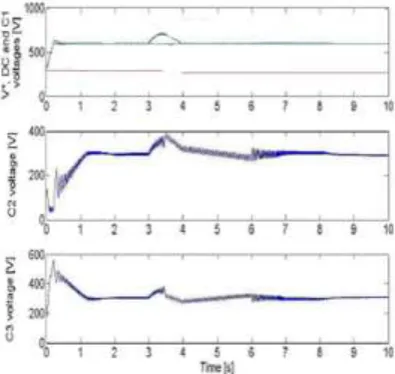
Fig 14(b) : Average Voltage across Capacitors Fig. 15 Torque Characteristics of
PMSM
To demonstrate that the proposed Z Source inverter is suitable for motor drives with single phase PM
synchronous machines, different perturbations on the drive were simulated. For example, it can be seen in Fig.
14(a) shows that the given voltage will be 300 and it will be shown in the above wave form the output voltage of
3 phase inverter is 600 v and from Fig 14(b) it explains that for a 10% voltage sag of the nominal DC voltage
source (fall from 300V to 270V) the C1 capacitor voltage remains unchanged. At the start of the converter one
of the two series capacitors (C2) is discharged and the second (C3) is charged with electrostatic energy. The C1
capacitor voltage smoothly follows the prescribed average DC link voltage; it has a very small overshoot. Even
if the prescribed average DC link voltage is raised gradually from 300V to 600V in 300ms, we do have some
216 | P a g e
spikes.In Fig. 14(b) can be seen that the instantaneous voltage across the load is asymmetrical, the positive partis two times greater than the negative part.
(a)
(b)
Fig 16(a) (b) The motor measured speed during acceleration.
The above Fig 15 can be shows the Torque characteristics of PMSM
Fig. 16(a)(b) shows the motor reference and measured speed while the motor accelerates to the nominal speed
3000 rpm in about 1.5 seconds. A breakpoint in the speed ramping is visible at 300 ms the moment when the C1
capacitor voltage reaches 600V. From this moment the motor has a steeper acceleration ramp, until it reaches
3000 rpm. A step load torque of 0.35 Nm is applied to the motor at t = 2 seconds until t = 8 seconds. This load
torque is not reflected in the capacitor voltages and the speed does not suffer a speed drop, which indicates that
the speed and current loops work well. At t = 3 seconds, the motor is decelerated to 33% of its nominal speed
for 3 seconds. A voltage boost is visible in the capacitor voltages during the deceleration process. At t = 6
seconds the motor speed increases again to the nominal speed. This time the acceleration time duration is longer
than the deceleration time duration because we have a torque load which goes to zero at t = 8 seconds and the
acceleration ramp gets steeper, again.
VI. CONCLUSION
The proposed modified Z-source three phase inverter is a possible solution for motor drives with three phase
permanent magnet synchronous machines. The converter is able to override the DC voltage sags. The inductors
peak currents are approximately twice the load peak current. The voltage boost of the intermediate DC link it
can be produced even if there are no “inactive states”. The results has been studied and observed in the
217 | P a g e
REFERENCES
[1] Fang Z. Peng “Z-Source Inverter,” IEE Transactions on Industry Applications, vol. 39, pp.
504-510, March-April 2003,.
[2] Fang Z. Peng, Miaosen Shen and Alan Joseph, “Z-Source Inverters, Control, and Motor Drive
Applications,” KIEE International Transactions on Electrical Machinery and Energy Conversion System, vol.
5-B, no. 1, pp. 6-12, 2005.
[3] Tran-Quang Vinh, Tae-Won Chun, Jung-Ryol Ahn and Hong-Hee Lee, “Algorithms for Controlling Both
the DC Boost and AC Output Voltage of the Z-Source Inverter,” in Proc. of the 32nd Annual Conference of
IEEE Industrial Electronics Society, IECON 2005, , pp. 970-974.
[4] Babak Farhangi and Shahrrokh Farhanghi, “Application of Z-Source Converter in Photovoltaic
Grid-Connected Transformer-less Inverter,” in Proc. of PELINCEC-2005, Warsaw, Poland, pp. 198-203.
[5] N. Mohan, W.P. Robbins, T.M. Underland, Power Electronics, John Wiley, 1995.
[6] F.Z. Peng, M.S. Shen, and Z.M. Qian, “Maximum Boost Control of the Z-Source Inverter,” inProc of.
IEEE-PESC’04, 2004, pp. 255-260.
[7] Poh Chiang Loh, D.M. Vilathgamuwa, C.J. Gajanayake, Yih Rong Lim, and Chern Wern Teo, “Transient
Modeling and Analysis of Pulse-Width Modulated Z-Source Inverter,” IEEE Transactions on Power
Electronics, vol. 22, pp. 498-507, March 2007.
[8] I. Boldea and S.A. Nasar, Electric Drives, Second edition, pp. 313-319, 380 386, 1998.
[9] F. Z. Peng and Miaosen Shen, Zhaoming Qian, “Maximum Boost Control of the Z-source Inverter,” in
Proc. of IEEE PESC 2004.
AUTHOR
B ASHOK KUMAR received the B.Tech Degree in Electrical and Electronics Engineering from G Pullaiah
college of Engineering and Technology, JNTU Anantapur, A.P. india in 2011. He is currently working towards
his M.Tech degree in Power electronics and electrical drives (PE&ED) in Mahatma Gandhi Institute of
Technology, Telangana, India. His interested areas are in the field of power systems, power electronics and also