© 2018, IRJET | Impact Factor value: 6.171 | ISO 9001:2008 Certified Journal | Page 2785
DESIGN OF LOW-POWER 2–4 MIXED-LOGIC LINE DECODERS WITH
CLOCK BASED TECHNIQUE
Ku. Priyanka M. Raut
1, Dr. R. M. Deshmukh
21
Post Graduate Student, Department of Electronics & Telecommunication, DRGIT&R, Amravati,
Maharashtra, India
2
Professor & Head, Department of Electronics & Telecommunication, DRGIT&R, Amravati, Maharashtra, India
---***---
Abstract
:
In these paper 2:4 decoder is discussed with 14transistor and 15 transistor LP, LPI, HP and HPI In present
scenario, power reduction is a major issue in the technology world. The low power design is major issue in high performance digital system, such as microprocessors, digital
signal processors (DSPs) and other applications. The chip
thickness and higher working pace prompts the plan of exceptionally complex chips with high clock frequencies. So planning of low power VLSI circuits is a mechanical need in these because of the popularity for compact purchaser gadgets item. In a microchip/microcontroller based frameworks, the most ordinarily utilized square is the direction set decoder. Subsequently; it will be not wrong on the off chance that we say the direction set decoder expends more power. Subsequently upgrading the energy of this square will be useful to decrease the general power utilization of the framework. Thus proposed plan for this paper is the use of adiabatic technique to reduce power consumption of instruction decoder. In this paper, we have proposed the design of 2:4 decoder with the use of adiabatic logic to reduce the power of the decoder and thus will help in power reduction of overall system.
Keywords
: LP, LPI, HP, HPI.I. INTRODUCTION
Presently a day's energy decrease is a noteworthy issue in the innovation world. The low power configuration is real issue in superior advanced framework, for example, chip, computerized flag processors (DSPs) and different applications. Chip thickness and higher working rate prompt the outline of extremely complex chips with high clock frequencies. So planning of low power VLSI circuits is a mechanical need in these because of the popularity for convenient buyer gadgets items. Decoder is a combinational rationale circuit that changes over a paired number an incentive to a related example of yield bits. Uses of decoders are wide; they incorporate information de-multiplexing, memory address interpreting, seven portion show and so on. A decoder is a straightforward circuit that changes over a code into an arrangement of signs. It is named as decoder since it changes the huge coded information into various basic blends which can be utilized to drive any flag, however we will start our investigation of encoders and decoders since they are more straightforward to outline. Dynamic guidelines happen just inside a sub-set of all directions.
In advanced frameworks, directions and also numbers are passed on by methods for double levels or heartbeat trains. A decoder is a rationale circuit that changes over a N-bit twofold information code into M yield lines to such an extent that just a single yield line is initiated for every last one of the conceivable blends of data sources. The decoder distinguishes or perceives or identifies a specific code. The N data sources can be a 0 or a 1, there are 2N conceivable info blends or codes. For every one of info mix just a single of the M yields will be dynamic (HIGH), all different yields will stay inert (LOW). A few decoders are intended to deliver dynamic LOW yield, while the various yields stay HIGH.
A typical kind of decoder is the line decoder which takes a n-digit twofold number and translates it into 2n information lines. The easiest is the 1-to-2 line decoder
© 2018, IRJET | Impact Factor value: 6.171 | ISO 9001:2008 Certified Journal | Page 2786 imperativeness dispersing in CMOS circuits is a direct
result of the charging and discharging of the center point capacitances of the circuits, present both as a stack and a parasite. Such bit of the total power scattered by a circuit is called dynamic power. To reduce the dynamic power, an elective method to manage the standard systems of vitality use diminish, named adiabatic trading has been proposed in the latest years. In such approach, the path toward charging and discharging the center point capacitances is passed on in a way so little measure of imperativeness is misused and a recovery of the essentialness set away on the capacitors is expert.
II. LITERATURE REVIEW
Since most recent couple of decades the fundamental difficulties were Area, cost, and execution. In any case, nowadays control is an imperative factor rather than cost, execution and region. The gadget which expends less power regardless of speed, for example, heart pacemaker, RFID and so forth chips away at the guideline of adiabatic rationale. The point of lessening in control utilization is application particular. The creators have endeavored to diminish the power by joining the adiabatic and reversible system [1]. The power devoured in customary CMOS configuration can be given as,
P=CL.VDD2. f
Here the power (P) is relative to exchanging recurrence (f), capacitance (CL), and square of supply voltage (VDD). Power utilization can be diminished by limiting force supply, capacitance and exchanging recurrence of activity. Yet, when this parameter decreases, it might decay the execution of the circuit. Configuration utilizing adiabatic rule helps in decreasing force utilization at the cost of reduce performance. A strategy in view of adiabatic method utilizes an air conditioner control supply as opposed to dc for vitality recuperation. Hypothetically adiabatic circuits devour zero power, it demonstrates vitality misfortune due to nonzero obstruction in the switches. There are such a large number of papers which depict distinctive kinds of adiabatic procedure, for example, ECRL, 2PASCL, PFAL and so on by which we can decrease control utilization of the circuit [2]. These strategies devour less power as contrast with different CMOS circuits.
III. DESIGN TECHNIQUE
1. Decoder
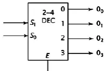
[image:2.595.378.487.84.157.2]Proposed 2-to-4 decoder with empower input is built with AND entryways, it turns out to be more prudent to create the decoder yield. A 2-to-4 decoder is empower when E=1. Reality table of a 2-to-4 decoder is given in Table I and the general square outline is appeared in figure 2. The Boolean door based execution of 2-to-4 decoder required four AND entryways and two NOT rationale entryways
Fig.1: General block diagram of 2-to-4 decoder
2. 2:4 Line Decoder
[image:2.595.368.502.301.351.2]Line decoders are fundamental circuits, widely used in the peripheral circuitry of memory arrays (e.g., SRAM) [7]–[9]. This brief develops a mixed-logic methodology for their implementation, opting for improved performance compared to single-style design.
[image:2.595.370.496.381.430.2]Table I: Truth Table of the 2–4 Decoder
Table II: Truth Table of The Inverting 2–4 Decoder
A 2–4 line decoder generates the 4 minterms D0−3 of 2 input variables A and B. Its logic operation is summarized in Table I. Depending on the input combination, one of the 4 outputs is selected and set to 1, while the others are set to 0. An inverting 2–4 decoder generates the complementary minterms I0−3, thus the selected output is set to 0 and the rest are set to
1, as shown in Table II. In conventional CMOS design, NAND and NOR gates are preferred to AND and OR, since they can be implemented with 4 transistors, as opposed to 6, therefore implementing logic functions with higher efficiency. A 2–4 decoder can be implemented with 2 inverters and 4 NOR gate Fig. 1(a), whereas an inverting decoder requires 2 inverters and 4 NAND gates Fig. 1(b), both yielding 20 transistors
[image:2.595.336.554.633.754.2](a) (b)
Fig. 2: 20-transistor 2–4 line decoders implemented with CMOS logic. (a) Non inverting NOR-based decoder. (b)
© 2018, IRJET | Impact Factor value: 6.171 | ISO 9001:2008 Certified Journal | Page 2787 3. Mixed Logic Line
[image:3.595.325.543.227.339.2]Transmission gate logic (TGL) can efficiently implement AND/OR gates [5], thus it can be applied in line decoders. The 2-input TGL AND/OR gates are shown in Fig. 3(a) and (b), respectively. They are full-swinging, but not restoring for all input combinations. Regarding PTL, there are two main circuit styles: those that use nMOS-only pass transistor circuits, like CPL [3], and those that use both nMOS and pMOS pass transistors, like DPL [4] and DVL [6]. The style we consider in this work is DVL, which preserves the full swing operation of DPL with reduced transistor count [10]. The 2-input DVL AND/OR gates are shown in Fig. 3(c) and (d), respectively. They are full swinging but non-restoring, as well.
Fig. 3: Three-transistor AND/OR gates considered in this work. (a) TGL AND gate. (b) TGL OR gate. (c) DVL AND
gate. (d) DVL OR gate.
Assuming that complementary inputs are available, the TGL/DVL gates require only 3 transistors. Decoders are high fan-out circuits, where few inverters can be used by multiple gates, thus using TGL and DVL can result to reduced transistor count. An important common characteristic of these gates is their asymmetric nature, ie the fact that they do not have balanced input loads. As shown in Fig. 3, we labelled the 2 gate inputs X and Y. In TGL gates, input X controls the gate terminals of all 3 transistors, while input Y propagates to the output node through the transmission gate. In DVL gates, input X controls 2 transistor gate terminals, while input Y controls 1 gate terminal and propagates through a pass transistor to the output. We will refer to X and Y as the control signal and propagate signal of the gate, respectively.
Using a complementary input as the propagate signal is not a good practice, since the inverter added to the propagation path increases delay significantly. Therefore, when implementing the inhibition (A_B) or implication (A_
+ B) function, it is more efficient to choose the inverted
variable as control signal. When implementing the AND (AB) or OR (A + B) function, either choice is equally efficient. Finally, when implementing the NAND (A_ + B_) or NOR (A_B_) function, either choice result to a complementary propagate signal, perforce.
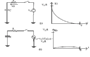
IV. ADIABATIC CIRCUITS
The term “adiabatic” refers to the thermodynamic process that exchanges no energy with environment, and therefore there is no occurrence of power or energy dissipation.
During the switching process, adiabatic technology reduces the power or energy dissipation and reuses some part of the energy by recycling it from the load capacitance.
Adiabatic circuits are basically low power circuits which use to conserve the energy by returning back its output energy to input, so that the same energy can be used for next operation.
[image:3.595.57.267.264.343.2]Fig. 4 and Fig. 5 shows the Charging and Discharging in conventional CMOS circuit and Adiabatic System.
[image:3.595.324.546.372.486.2]Fig. 4: Charging and Discharging in Conventional system
Fig.5: Charging and Discharging in Adiabatic system
Fig. 6: (a) Switching of CMOS (b) Switching of Adiabatic Logic
Adiabatic circuits aims to conserve the charges by following essential rules
1) Avoiding turning on of transistor whenever there is a potential difference across the drain and source (VDS>0).
[image:3.595.337.524.523.642.2]© 2018, IRJET | Impact Factor value: 6.171 | ISO 9001:2008 Certified Journal | Page 2788 3) The current should not pass through diode.
Adiabatic Logic Types
V. SIMULATION
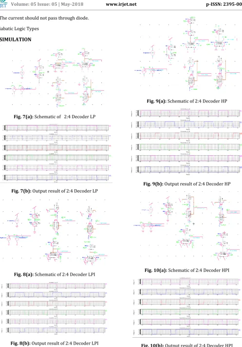
Fig. 7(a): Schematic of 2:4 Decoder LP
Fig. 7(b): Output result of 2:4 Decoder LP
Fig. 8(a): Schematic of 2:4 Decoder LPI
Fig. 8(b): Output result of 2:4 Decoder LPI
Fig. 9(a): Schematic of 2:4 Decoder HP
Fig. 9(b): Output result of 2:4 Decoder HP
Fig. 10(a): Schematic of 2:4 Decoder HPI
[image:4.595.49.547.50.762.2]© 2018, IRJET | Impact Factor value: 6.171 | ISO 9001:2008 Certified Journal | Page 2789
[image:5.595.40.283.136.203.2]EXPECTED RESULT
Table 1: Depicts various decoder with conventional technique.
Sr. No Parameters Leakage Current Power Dissipation
1 2:4 LP 678.0223 n 3.39011 µ
2 2:4 HP 677.80409 n 3.39902 µ
3 2:4 LPI 716.00418 n 3.58002 µ
4 2:4 HPI 716.0311 n 3.58016 µ
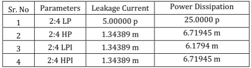
Table 2: Depicts various decoder with adeabetic technique.
Sr. No Parameters Leakage Current Power Dissipation
1 2:4 LP 5.00000 p 25.0000 p
2 2:4 HP 1.34389 m 6.71945 m
3 2:4 LPI 1.34389 m 6.1794 m
4 2:4 HPI 1.34389 m 6.71945 m
CONCLUSION:
The new design with respect to adiabatic technique reduce
the power dissipation.Adiabatic design is an energy efficient way of design for low power circuits. The low
power dissipation is archived by using adiabatic technique.
REFERENCES:
1) Dimitrios Balobas and Nikos Konofaos, “Design of Low-Power High-Performance 2–4 and 4–16 Mixed-Logic Line Decoders”, IEEE TRANSACTIONS ON CIRCUITS AND SYSTEMS—II: EXPRESS BRIEFS, VOL. 64, NO. 2, FEBRUARY 2017.
[2] N. H. E. Weste and D. M. Harris, CMOS VLSI Design, a Circuits and v Systems Perspective, 4th ed. Boston, MA, USA: Addison-Wesley, 2011.
[3] R. Zimmermann and W. Fichtner, “Low-power logic styles: CMOS versus pass-transistor logic,” IEEE J. Solid State Circuits, vol. 32, no. 7, pp. 1079–1090, Jul. 1997.
[4] K. Yano et al., “A 3.8-ns CMOS 16 × 16-b multiplier using complementary pass-transistor logic,” IEEE J. Solid-State Circuits, vol. 25, no. 2, pp. 388–393, Apr. 1990.
[5] M. Suzuki et al., “A 1.5 ns 32b CMOS ALU in double pass-transistor logic,” in Proc. IEEE Int. Solid-State Circuits Conf., 1993, pp. 90–91.
[6] X. Wu, “Theory of transmission switches and its application to design of CMOS digital circuits,” Int. J. Circuit Theory Appl., vol. 20, no. 4, pp. 349–356, 1992.
[7] V. G. Oklobdzija and B. Duchene, “Pass-transistor dual value logic for low-power CMOS,” in Proc. Int. Symp. VLSI Technol., 1995, pp. 341–344.
[8] M. A. Turi and J. G. Delgado-Frias, “Decreasing energy consumption in address decoders by means of selective pre charge schemes,” Micro electron. J., vol. 40, no. 11, pp. 1590–1600, 2009.
[9] V. Bhatnagar, A. Chandani, and S. Pandey, “Optimization of row decoder for 128 × 128 6T SRAMs,” in Proc. IEEE Int. Conf. VLSI-SATA, 2015, pp. 1–4.
[10] A. K. Mishra, D. P. Acharya, and P. K. Patra, “Novel design technique of address decoder for SRAM,” Proc. IEEE ICACCCT, 2014, pp. 1032–1035.
[11] D. Markovi´c, B. Nikoli´c, and V. G. Oklobdžija, “A general method in synthesis of pass-transistor circuits,” Micro electron. J., vol. 31, pp. 991–998,2000.
[image:5.595.38.284.246.313.2]