EAI
European Alliance for Innovationon Industrial Networks and Intelligent Systems
Research Article
1
Energy Efficient Dual Issue Embedded Processor
Hanni Lozano
1and Mabo Ito
1,*
1
University of British Columbia, Vancouver, Canada
Abstract
While energy efficiency is essential to extend the battery life of embedded devices, performance cannot be ignored. High performance superscalar embedded processors are more energy efficient than low performance scalar processors, however, they consume more power which is very limited in battery operated deeply embedded industrial devices. In this paper we propose an energy efficient dual issue embedded processor that can deliver up to 60% improvement in IPC (instruction-per-cycle) performance with less than 20% increase in power consumption compared to a single issue scalar processor. In contrast to traditional multi-issue embedded processors that use power intensive superscalar techniques to extract instruction-level parallelism from applications, the proposed processor uses simple hardware techniques to resolve instruction scheduling conflicts. The processor is optimized for implementation on a low cost FPGA which makes it a suitable candidate for cost sensitive embedded industrial applications.
Keywords: embedded processor, energy efficiency.
Received on 24 February 2015, accepted on 07 November 2015, published on 01 January 2016
Copyright © 2016M. Ito and H. Lozano, licensed to EAI. This is an open access article distributed under the terms of the Creative Commons Attribution licence (http://creativecommons.org/licenses/by/3.0/), which permits unlimited use, distribution and reproduction in any medium so long as the original work is properly cited.
doi: 10.4108/eai.1-1-2016.150814
1. Introduction
The challenge in designing energy efficient embedded devices is how to increase the device computational performance while using the least amount of power. Most embedded communication devices like remote sensors in industrial applications operate on batteries and in some cases these batteries cannot be replaced so frequently or at all. In these cases, alternative energy sources like energy-harvesting are used. However, energy-energy-harvesting techniques supply very limited amount of power; for example, a 36.5 x 64 mm 3-Volts solar panel from PowerFilm delivers 66 mWatts in 100% sun and less than 20 mWatts in 25% sun which is a typical threshold intensity used by portable devices [1]. To put these numbers into perspective, the single issue ARM Cortex-M4 scalar processor consumes 16.5 mWatts at 500 MHz whereas the dual issue ARM Cortex-A7 superscalar processor consumes 50 mWatts at 500 MHz [5], well above the 20 mWatts that the PowerFilm solar panel can deliver.
Although the Cortex-M4 scalar processor consumes much lower power than the Cortex-A7, it can only issue a single instruction per cycle which limits its performance potential. In contrast, the Cortex-A7 superscalar processor can issue multiple instructions per cycle which allows it to complete tasks faster than scalar processors and, consequently, turn off unused resources to save energy in the long run. Overall, the Cortex-A7 delivers 1.5x higher performance than the Cortex-M4 while consuming 3x more power [5]. Because the Cortex-A7 consumes more power than the scalar Cortex-M4 processor, therefore, it cannot be used in battery operated embedded devices or embedded devices powered by an energy harvesting source such as the PowerFilm solar panel mentioned earlier. The challenge for next generation embedded industrial devices is how to balance the increasing demand for higher performance with longer battery life. The ideal solution is to design an embedded processor that can deliver performance comparable to a superscalar processor while consuming the same, or as close as possible, amount of power as a single issue scalar processor.
*
Corresponding author Email: [email protected]
and Intelligent Systems 09 2015 -01 2016 | Volume
3 | Issue 6 | e4
EAI
European Alliancefor Innovation 2
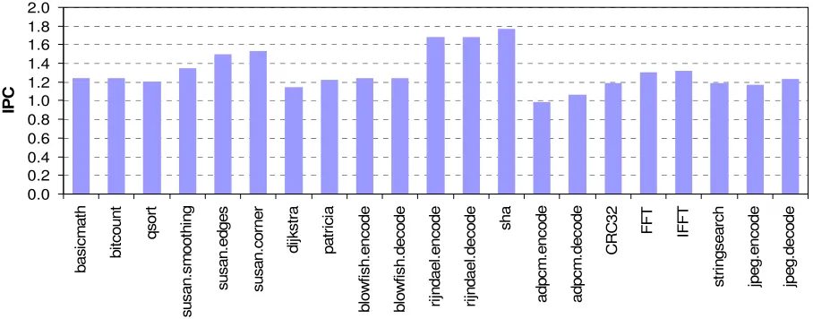
0.0 0.2 0.4 0.6 0.8 1.0 1.2 1.4 1.6 1.8 2.0 b a s ic m a th b it c o u n t q s o rt s u s a n .s m o o th in g s u s a n .e d g e s s u s a n .c o rn e r d ijk s tr a p a tr ic ia b lo w fi s h .e n c o d e b lo w fi s h .d e c o d e ri jn d a e l. e n c o d e ri jn d a e l. d e c o d e s h a a d p c m .e n c o d e a d p c m .d e c o d e C R C 3 2 F F T IF F T s tr in g s e a rc h jp e g .e n c o d e jp e g .d e c o d e IP C
Figure 1. IPC performance of an ideal dual issue embedded processor.
The reason superscalar processors consume more power than scalar processors is because they use aggressive and complex hardware techniques, such as out-of-order issue, speculative execution, etc., to issue more than one instruction per cycle. The amount of effort needed to issue multiple instructions per cycle depends on how much instruction level parallelism (ILP) is contained in the target applications. Instruction level parallelism is a measure of the number of independent instructions that can be issued in parallel every cycle independent of any other external factors such as hardware resource limitations. In applications with high ILP, the processor doesn’t need to use aggressive techniques to extract available parallelism in the code, instead simple scalar techniques will suffice. The amount of ILP varies between applications. For example, references [23] and [24] showed that general purpose applications have an average IPC of four regardless of the type of CPU used, whereas reference [9] showed that embedded applications can achieve IPC higher than two using a high-end four-instruction wide superscalar Compaq Alpha 21264 processor.
Figure 1shows the max IPC for a number of embedded applications using an ideal two-instruction wide in-order scalar processor with four pipeline stages, perfect branch prediction, unlimited number of registers, unlimited number of memory ports and unlimited number of functional units. Results indicate that on average 1.5 instructions are issued every cycle. Benchmarks that have long basic blocks of code such as susan.edges, susan.corner, rijndael and sha tend to have much higher ILP which translates to higher IPC because it is easier for the processor to locate independent instructions that it can issue in parallel. The IPC performance of these benchmarks is well above average; it is actually close to the max issue capacity of a dual issue processor. These results confirm that there is an abundance of ILP in embedded programs that can be easily extracted using minimal effort.
We propose a dual issue embedded processor that uses simple hardware techniques to extract available ILP from applications. The proposed processor delivers up to 60% higher IPC than a single issue scalar processor while using only 20% more power. The average increase in IPC is around 40%. The proposed processor can fetch, decode and issue two instructions simultaneously every cycle. The dual issue processor uses approximately 30% more logic gates than the single issue processor when implemented on a low cost FPGA which helps keep the power consumption low. The main reason we limited ourselves to dual-issue processors is because increasing the processor width beyond two instructions is very difficult to achieve, especially when targeting an FPGA. The main source of difficulty is the implementation of a multi-port register file (RF). The RF of a four instructions wide processor uses four write ports and eight read ports whereas FPGA memories as well as most of low cost standard embedded memories have only two ports that can be configured as read/write ports or one read port and one write port. In section 4 we will explore in detail the implementation of a multi-port register file using dual port memories.
The main characteristics of the proposed dual issue scalar processor are:
•A short in-order 4-stage pipeline that executes a rich 32-bit RISC instruction set based on the MIPS instruction set [2].
•Tightly coupled program and data memories with zero-wait states using Harvard architecture.
•A static branch predictor that performs within a 5% range of an ideal branch predictor.
•Result forwarding scheme that uses FPGA built-in features without any additional external logic.
•An optimized multi-port register file (RF) that uses a novel memory redundancy technique.
and Intelligent Systems 09 2015 -01 2016 | Volume
3 | Issue 6 | e4
EAI
European Alliancefor Innovation 3
A custom cycle accurate C simulator that models a single issue RISC processor and a multi-issue superscalar RISC processor is used to evaluate architectural design decisions in the early phases of the design process. All the processor implementation details such as issue width, number of memory ports, number of functional units, etc. can be configured statically by the user. Once all the processor features were optimally evaluated, the processor is implemented in a low cost FPGA to measure performance, power consumption and resource usage.
The paper is organized according to the following outline. Related works are discussed next in section 2. The simulation environment including benchmarks and base processor architectural details are described in section 3. A detailed description of the dual issue processor is included in section IV. Section V discusses results and the conclusion is presented in section VI.
2. Related Work
2.1. Processor Survey
These processors are either used as standalone embedded processors or as embedded cores in multi-core processors. For our study we limit our analysis to standalone dual issue in-order processors that target the low cost and low power embedded market. This type of embedded processors are characterized by single thread execution, the use of tightly coupled data and instruction memories with optional zero wait state access, a short pipeline usually three or four stages deep, simple static or no branch prediction, in-order instruction issue and single cycle execution for most instructions. Table 1 compares a number of academic and commercial processors. The main observations are:
• The majority of embedded processors listed in Table 1 use a RISC instruction set. The only exception is Intel ATOM embedded processor which uses a CISC instruction set. Despite the popular belief that RISC processors are more efficient than CISC processors, a recent study comparing RISC and CISC has shown that the choice of an instruction set has no impact performance nor energy efficiency [25].
• The PATMOS processor is designed for academic research on time-predictable multi-core architecture and hard real-time embedded systems. It can be configured as a standalone processor or as a core in a multi-core processor.
• The LEON3 is part of the LEON family of processors originally designed by the European Space Agency (ESA) and currently maintained by Gaisler (www.gaisler.com).
• The NIOS-II and MicroBlaze are FPGA soft cores provided by Altera and Xilinx, respectively. These cores come in different configurations and features and are mostly used as micro-controller rather than fully fledged embedded processors.
•Most processors have very short pipelines, three to five stages. The exception again is Intel ATOM processor which has a 16-stage deep pipeline. The reason is that the ATOM processor dynamically converts complex CISC instructions into RISC-like micro-operations using multiple pipeline stages.
•A wider pipeline does not necessarily translate to higher performance. Dual issue ATOM and PATMOS have a much lower Coremark/MHz score than single issue microAptive and Cortex-M4. The performance of PATMOS dual issue version is only 7% higher than the performance of PATMOS single issue version [26]. The authors in [26] attribute this weak performance to deficiencies in PATMOS instruction set and compiler. •The ATOM processor Coremark performance is poor
due to the additional delay caused by the long 16-stage pipeline; long latency operations which are common in the Coremark benchmark incur an additional penalty in processors with a deep pipeline similar to ATOM [1] [8]. In contrast, the Cortex-M4 which has a short 3-stage pipeline can deliver a much higher Coremark performance than ATOM despite its smaller size. •The microAptive and ARM Cortex-M4 cores have the
highest Coremark/MHz score of all processors. The biggest differentiating factor is that these two processors are modern RISC cores that combine a number of advanced architectural features such as complex addressing, traditionally used in CISC processors, with RISC simple and efficient implementation.
2.2. Other Areas of Embedded Processor
Design
The majority of academic research in the area of embedded processor architecture focuses on superscalar techniques, with some of the work specifically targeting FPGA implementation [10]. Some of the works investigated the use of simple scalar cores in multi-core processors targeting standard-cell implementations [11] as well as FPGA [13] to speed up the execution of multi-threaded applications. Some research looked into specific aspect of the architecture in isolation from other architectural elements, for example the design of the register file [12]. Reference [12] gives a brief introduction for the different techniques that implement multi-port register file using standard two port memories. Reference [17] combined several of these techniques to optimize the implementation of a 6-write and 12-read ports register file used in a wide superscalar processor. However, their technique similar to most previous multi-port techniques requires an additional pipeline stage to read data from the register file. Other works investigated the design of embedded processors that target specific applications such as biomedical [18] or Smartgrid [19].These processors tend to be heavily customized and more closely resemble an application-specific-integrated-circuit (ASIC) than a general purpose processor. Our focus is on multi-issue techniques for energy efficient embedded processors.
and Intelligent Systems 09 2015 -01 2016 | Volume
3 | Issue 6 | e4
EAI
European Alliancefor Innovation 4
Table 1. List ofacademic and commercial embedded processors. ISA refers to the processor/core instruction-set-architecture which can be either CISC (Complex-Instruction-Set Computer) or RISC (Reduced-Instruction-Set Computer).
Processor Core ISA Instruction Width (bits)
Issue Width (instructions)
Number of Stages
Instruction Issue
Coremark/MHz [7]
PATMOS [26] RISC 32 2 5 in-order 1.90
LEON3 [20] RISC 32 1 7 in-order 1.80
Altera NIOS-II (s/f) [3] RISC 32 1 5 - 6 in-order 1.60
Xilinx MicroBlaze [4] RISC 32 1 3 - 5 in-order 1.90
Imagination Tech.
microAptive [2] RISC 32 1 5 in-order 3.44
Intel ATOM [6] CISC 32 2 16 in-order 2.28
ARM Cortex-M4 [5] RISC 32 1 3 in-order 3.40
3. Simulation Environment
3.1. Benchmarks
The MiBench benchmark suite [9] is used to cover a wide range of embedded applications grouped into six categories: automotive, consumer, network, office, security and telecom. All benchmark programs are cross compiled and statically linked on a Linux host machine using a GNU MIPS32 cross-compiler version 4.4.3 and a GNU lib version 2.4. Each benchmark program is run to completion using the MiBench provided large data set and outputs are compared to the outputs generated by
executing the same benchmark program natively on the Linux host machine. Table 2 lists the benchmark programs and the total number of instructions executed for each benchmark. The binary image size of each benchmark is listed in the last column of Table 2. These numbers represent the minimum size in bytes that each program occupies in program memory for a bare metal implementation with minimal operating system (OS) support.
0% 10% 20% 30% 40% 50% 60% 70% 80% 90% 100%
b
a
s
ic
m
a
th
b
itc
o
u
n
t
q
s
o
rt
s
u
s
a
n
.s
m
o
o
th
in
g
s
u
s
a
n
.e
d
g
e
s
s
u
s
a
n
.c
o
rn
e
r
d
ijk
s
tr
a
p
a
tr
ic
ia
b
lo
w
fis
h
.e
n
c
o
d
e
b
lo
w
fis
h
.d
e
c
o
d
e
ri
jn
d
a
e
l.e
n
c
o
d
e
ri
jn
d
a
e
l.d
e
c
o
d
e
s
h
a
a
d
p
c
m
.e
n
c
o
d
e
a
d
p
c
m
.d
e
c
o
d
e
C
R
C
3
2
F
F
T
IF
F
T
s
tr
in
g
s
e
a
rc
h
jp
e
g
.e
n
c
o
d
e
jp
e
g
.d
e
c
o
d
e
T
o
ta
l
In
s
tr
u
c
ti
o
n
s
IMUL IDIV IALU SHIFT CONTROL MEM REGMOVE FP_ARITH FP_LOGIC
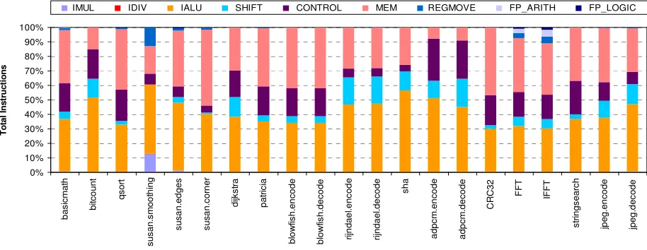
Figure 2. Instruction type distribution using the large data set per MiBench benchmark (IMUL=integer multiply, IDIV=integer division, IALU=integer ALU as listed in the text, SHIFT=logical and arithmetic shifts, CONTROL=conditional & unconditional branch, MEM=memory load/store, REGMOVE=register move, FP_ARITH=floating point arithmetic operations and FP_LOGIC=floating point logic operations).
and Intelligent Systems 09 2015 -01 2016 | Volume 3 | Issue 6 | e4
EAI
European Alliancefor Innovation 5
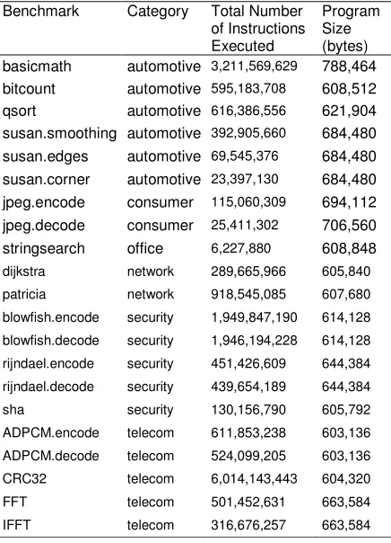
Table 2. MiBench benchmark list with the corresponding total number of instructions executed per run using the large data set and each program binary image size in bytes.
Benchmark Category Total Number of Instructions Executed
Program Size (bytes) basicmath automotive 3,211,569,629 788,464 bitcount automotive 595,183,708 608,512 qsort automotive 616,386,556 621,904 susan.smoothing automotive 392,905,660 684,480 susan.edges automotive 69,545,376 684,480 susan.corner automotive 23,397,130 684,480 jpeg.encode consumer 115,060,309 694,112 jpeg.decode consumer 25,411,302 706,560 stringsearch office 6,227,880 608,848
dijkstra network 289,665,966 605,840
patricia network 918,545,085 607,680
blowfish.encode security 1,949,847,190 614,128
blowfish.decode security 1,946,194,228 614,128
rijndael.encode security 451,426,609 644,384
rijndael.decode security 439,654,189 644,384
sha security 130,156,790 605,792
ADPCM.encode telecom 611,853,238 603,136
ADPCM.decode telecom 524,099,205 603,136
CRC32 telecom 6,014,143,443 604,320
FFT telecom 501,452,631 663,584
IFFT telecom 316,676,257 663,584
Figure 2 shows the distribution per operation type for each MiBench benchmark program. The Integer Arithmetic and Logic Unit (IALU) category contains the following combination of integer arithmetic and logical operations: integer addition, integer subtraction, bitwise logical operations and operands comparison. The SHIFT category contains all bitwise logical and arithmetic shift operations which in some benchmarks represent 10% of the total number of operations. There are several observations to be drawn from the results of Figure 2:
• The percentage of floating point instructions in the MiBench benchmark programs does not exceed 0.5%. Only the FFT and IFFT benchmarks have a measurable percentage of floating point instructions equal to 4% and 7% respectively. Therefore, floating point operations are emulated in software instead of using a dedicated floating point functional unit in hardware.
• Ninety-five percent (95%) of instructions in the benchmark programs, except the susan.smoothing benchmark, are distributed between only three types of operations: ALU operation which includes logical and arithmetic shift operations, memory operations and control operations.
• The percentage of integer multiplications does not exceed 0.2% which eliminates the need to add a second multiplier in the dual-issue version of the processor. Using a single multiplier constitute a major reduction in the size and power consumption of the dual-issue processor.
• The average percentage of integer ALU operations is approximately 50% and more than 70% of ALU operations are addition and subtraction operations. These results are very meaningful for the dual-issue processor because instead of duplicating the complete ALU unit which happens to be the largest logic block in the processor, we just duplicate the adder to keep number of gates and power consumption low without degrading performance. • Forty percent (40%) of instructions in almost half the
benchmarks are memory load and store instructions. These numbers show the importance of having a high speed interface between the data memory and the processor core. In our case we use tightly coupled memories with zero wait state to allow memory accesses to execute in a single cycle on a 4-stage pipeline processor.
• The percentage of conditional and unconditional control instructions varies from 5% to 25%. The adpcm benchmarks contains the highest number of control operations of all benchmarks due to the predominance of short loops that convert 16-bit linear PCM speech samples to 4-bit samples. • The high percentage of REGMOVE operations in the
susan.smoothing benchmark, as well as in the basicmath, susan.edges and susan.corner benchmark but to a much lesser degree, is a result of scaling and moving 64-bit multiplication results into 32-bit registers. In the FFT and IFFT benchmarks REGMOVE instructions are used to move 64-bit floating point results into 32-bit registers.
• The distribution of instructions in embedded applications closely resembles the distribution of instructions in general purpose applications reported in [23] and [24]. The only minor difference is the number of control operations in general purpose applications is marginally higher.
NOP (no-operation) instructions are used in the MIPS32 ISA to fill empty instruction slots and branch delay slots in case the compiler is unable to find valid instructions to schedule in these slots. Branch delay instructions are instructions that immediately follow a branch instruction and must be executed before the branch is executed, i.e. taken or not taken. The percentage of NOP instructions can be as high as 30% the total number of instructions in a program. The jpeg.encode benchmark has the highest percentage of NOP instructions in the MiBench benchmarks at approximately 25%, while the average percentage is only around 15%. The drawback of NOP operations is that they insert bubbles in the pipeline which results in a considerable loss in performance and energy efficiency.
and Intelligent Systems 09 2015 -01 2016 | Volume 3 | Issue 6 | e4
EAI
European Alliancefor Innovation 6
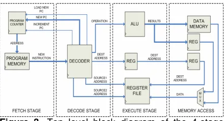
Figure 3. Top level block diagram of the 4-stage base processor.
3.2. Base Processor Architecture
Figure 3 shows the top level diagram for the base scalar processor. A custom cycle accurate simulator written in C is used to conduct a thorough evaluation of different architectural features as well as to collect run-time statistics (e.g. total number of cycles, number of mispredicted branches, etc.). All the processor features such as the number of pipeline stages, branch prediction technique, etc. can be configured by the user dynamically at runtime. The simulator models a 32-bit RISC processor with a Harvard memory configuration and 4-stage pipeline: fetch, decode, execute and memory access. We experimented with different pipeline stages ranging from three up to six and found out that a four stage pipeline is less complex to implement in hardware than a five or six stage pipelines and produced better IPC performance, 20% on average, than a three stage pipeline which was severely impacted by frequent pipeline stalls from multi-cycle memory access operations. Figure 4 shows the percentage of increase in IPC for a 4-stage pipeline compared to a 3-stage pipeline. Benchmark programs that contain a large percentage of memory operations and a low percentage of control operations such as susan.edges and susan.corner benefited the most from adding a dedicated pipeline stage for memory access. The increase in IPC in these two benchmarks ranges from 30% to 40% respectively which is remarkable considering that the hardware overhead for adding a fourth pipeline stage is minimal. Benchmark programs with a high percentage of memory and control operations such as qsort and FFT achieved a 20% increase on average but did not perform as well as the susan benchmarks because the frequent interruption of the pipeline by the control operations inserted too many bubbles in the pipeline that eliminated any gain from adding the extra pipeline stage.
The processor implements the complete MIPS32 instruction set [2] excluding all floating point and co-processor instructions. Instruction distribution results presented in the previous section clearly showed that embedded benchmark programs, with the exception of the FFT and IFFT benchmarks, contain insignificant numbers of floating point operations (the average percentage is around 0.5%) which does not justify adding a dedicated floating point functional unit in the processor.
1.00 1.05 1.10 1.15 1.20 1.25 1.30 1.35 1.40 1.45 1.50 b a s ic m a th b itc o u n t q s o rt s u s a n .s m o o th in g s u s a n .e d g e s s u s a n .c o rn e r d ijk s tr a p a tr ic ia b lo w fis h .e n c o d e b lo w fis h .d e c o d e ri jn d a e l.e n c o d e ri jn d a e l.d e c o d e s h a a d p c m .d e c o d e a d p c m .e n c o d e C R C 3 2 F F T IF F T s tr in g s e a rc h jp e g .e n c o d e jp e g .d e c o d e a v e ra g e In c re a s e i n I P C
Figure 4. Increase in IPC for a 4-stage processor compared to a 3-stage processor.
ALU
The processor largest block is the ALU which consumes 60% of the processor total logic gates. The ALU includes a 32-bit fixed-point adder with overflow detection, a 32-bit fixed-point multiplier with a 64-bit accumulator, a 32-bit logic unit that performs bitwise operations and a 32-bit shift unit for bitwise logical and arithmetic shifts. All ALU operations excluding division which is emulated in software, execute in a single cycle. In the FPGA, the 32-bit multiplier is implemented using the FPGA hardwired embedded multipliers which reduces the total logic elements (LE) count by 20% compared to implementing our own multiplier using standard logic. The drawback is that several 18-bit multipliers need to be cascaded together to perform 32-bit wide multiplications which increases the latency of multiplication operations and reduces the processor clock top speed by almost 40%, from 100 MHz down to 60 MHz.
Instruction Decoder
The instruction decoder main function is to extract the relevant fields, e.g. addresses of the source and destination registers, from newly fetched instructions and generate the control signals needed to perform the operation associated with each instruction. The decoder is also responsible for detecting control instructions, calculating the branch target address using a dedicated 32-bit adder and forwarding the result to the instruction fetch unit to update the program counter for the next fetch cycle. For conditional branches, a branch recovery address is calculated and temporarily stored in a register in case the branch prediction outcome is wrong and the processor needs to resume normal program execution. In an always-taken static predictor, the branch recovery address is calculated by incrementing the current program counter (PC) by two instructions slots and storing the result in the branch recovery address register. An alternative solution would be to store the current PC in the branch recovery address register and increment when a branch outcome is mispredicted. In a 4-stage pipeline, the decode and execute stages are just one cycle apart which means that the calculation of the branch recovery address can be easily done one cycle later in the ALU instead of the decoder. Despite covering a number of functions, the instruction decoder uses less than 5% the total number of logic gates in the processor.
and Intelligent Systems 09 2015 -01 2016 | Volume
3 | Issue 6 | e4
EAI
European Alliancefor Innovation 7
0.0 0.1 0.2 0.3 0.4 0.5 0.6 0.7 0.8 0.9 1.0 b a s ic m a th b itc o u n t q s o rt s u s a n .s m o o th in g s u s a n .e d g e s s u s a n .c o rn e r d ijk s tr a p a tr ic ia b lo w fis h .e n c o d e b lo w fis h .d e c o d e ri jn d a e l.e n c o d e ri jn d a e l.d e c o d e s h a a d p c m .e n c o d e a d p c m .d e c o d e C R C 3 2 F F T IF F T s tr in g s e a rc h jp e g .e n c o d e jp e g .d e c o d e IP C
no-pred static-taken static-not-taken perfect
Figure 5. IPC performance of the base processor using different branch prediction techniques (no-pred=no branch prediction, static-taken=static predictor with default taken prediction, static-not-taken=static predictor with default no-taken prediction, perfect = perfect branch prediction).
Branch Prediction
All branch instructions, except for the indirect jump instructions which store the target address in a general purpose register, are executed during the decode stage. A branch predictor allows conditional branches to be dispatched before they are executed to prevent stalling the pipeline. Figure 5 compares IPC results of a single issue processor using: a static branch predictor with two prediction heuristics (always taken and always no-taken), a processor without a branch predictor (no-pred) and a processor with a perfect predictor (perfect). Results reveal that IPC degrades by as much as 10% when no branch predictors are used. On the other hand, a simple static predictor can boost the average IPC performance to within 5% the IPC performance of a perfect predictor. Simulation results also reveal that the always taken heuristic performs better than the always not-taken heuristic by an average of 2% which agrees with reference [18] results. Figure 6 shows the IPC performance for each heuristic per benchmark. Although the difference is insignificant, we decided to use the always taken heuristic for the rest of our simulations. A more idealistic solution would be to make the choice of heuristic selectable by the user. 0% 10% 20% 30% 40% 50% 60% 70% 80% 90% 100% b a s ic m a th b it c o u n t q s o rt s u s a n .s m o o th in g s u s a n .e d g e s s u s a n .c o rn e r d ijk s tr a p a tr ic ia b lo w fi s h .e n c o d e b lo w fi s h .d e c o d e ri jn d a e l. e n c o d e ri jn d a e l. d e c o d e s h a a d p c m .e n c o d e a d p c m .d e c o d e C R C 3 2 F F T IF F T s tr in g s e a rc h jp e g .e n c o d e jp e g .d e c o d e B ra n c h P re d ic ti o n S u c c e s s R a te taken not-taken
Figure 6. IPC results for a static branch predictor using an always taken and always not-taken heuristics.
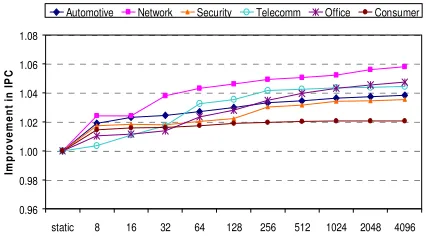
Performance improves by as little as 5% when the static branch predictor is upgraded to a bimodal dynamic predictor with a 2-bit saturating history counter. Figure 7 shows the gain in IPC for a bimodal branch predictor using different branch history table (BHT) sizes relative to the static predictor. A fully-associative bimodal predictor with a 4K direct-mapped BHT achieves a 2% to 6% gain in IPC compared to the static predictor which matches very closely the performance of a perfect predictor. However, a BHT with 4K entries is too big and consumes too much power to be used in a low power embedded processor. A BHT with a more realistic number of entries of 64 or 128 achieves a 2% to 4% improvement in IPC, respectively, which is too small to justify the added logic and complexity. Also, accessing the BHT requires an additional pipeline stage between decode and execute stages which increases the number of speculative instructions that has to be flushed out from the pipeline when a branch is mispredicted. An increase in the number of missepculated instructions reduces the energy efficiency of the processor which is critical in battery operated embedded devices. A shorter pipeline with fewer missepculated instructions is also the reason why a simple branch predictor performs so well.
0.96 0.98 1.00 1.02 1.04 1.06 1.08
static 8 16 32 64 128 256 512 1024 2048 4096
Im p ro v e m e n t in I P C
Automotive Network Security Telecomm Office Consumer
Figure 7. IPC results for a bimodal branch predictor relative to IPC results of a static predictor using different BHT sizes.
and Intelligent Systems 09 2015 -01 2016 | Volume
3 | Issue 6 | e4
EAI
European Alliancefor Innovation 8
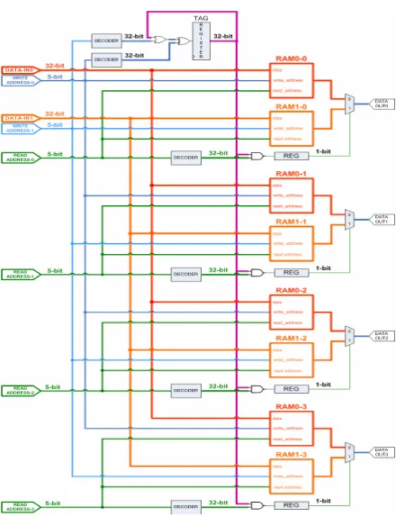
Figure 8. Multi-port emulation techniques using dual-port modules.
Register File
The RF has one write port and two read ports and contains 32 general purpose registers each 32-bit wide. However, standard embedded memories have only two ports that can be configured as read ports or write ports. Adding three or more ports requires the design of custom memories. An alternative solution is to emulate multi-read and multi-write memories using basic two port memories [10]. There are three different techniques, depicted in Figure 8, for emulating multi-port memories using standard dual-port memories:
• Replication technique is used to emulate single write and multiple read memories. The RAM module is duplicated once per read port. A write is broadcasted to all the modules at once. Data is read individually from each module.
• Banking technique can emulate multiple write and multiple read memories by dividing the RAM module into as many RAM sub-modules as there are read and write ports. Dividing the RF into sub-modules each hardwired to a read/write pair of ports means that data stored in one sub-module cannot be read at any read port which makes the data “non-coherent”.
• Pumping technique supports a variable number of write and read ports by clocking the RAM module at higher speed than data writes and reads. This technique is also known as “time-multiplexing”. Clocking the RAM module at higher speed than the write and read ports might not be feasible if the read and write ports are already operating at the processor max speed.
We chose a combination of the replication and the banking methods (Figure 9) because it uses the least amount of logic resources compared to the other surveyed techniques for a 1-write and 2-read RF. The drawback is that we need double the number of memory bits. However, the 32-entry by 32-bit register file uses a total of 2-Kbits which can easily fit in a single embedded memory block on the FPGA.
Figure 9. One write and two read ports RF.
Result Bypass
When a true dependency exists between two consecutive instructions, results must be made available to the decode stage as soon as instruction execution finishes (see diagram below). Otherwise, program execution has to be stalled for at least one cycle until the result is written back to the register file or data memory before it can be retrieved by the consuming instruction. The solution is to forward the result directly to the decode stage while, simultaneously, writing it back to the destination register or memory location.
This technique is known as result bypass and is usually implemented using a multiplexer and logic comparators. For the FPGA implementation, instead of using dedicated bypass logic we use the write-through built-in feature that exists in FPGA embedded memories [3] [4]. This technique embeds the external bypass multiplexers and logic gates into the memory modules themselves which becomes transparent to the end user. Using the write-through feature, the new data can be written to a memory location and read from the same memory location at the exact same clock edge. Although the write-through technique uses approximately the same amount of logic as the traditional bypass method with the external multiplexers and logic gates, its biggest advantage is it simplicity and transparency to the user.
3.3. FPGA Implementation
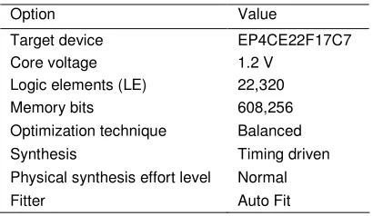
The base scalar processor is coded in Verilog and implemented on an Altera Cyclone-IV E 22K using Altera QuartusII web edition toolset version 13.0 [3]. Table 3 lists the FPGA features and compilation options used for the base processor. The compilation uses a timing driven place and route algorithm with balanced optimization technique (giving area and speed equal weights) and normal physical synthesis effort for post place and route optimization.
and Intelligent Systems 09 2015 -01 2016 | Volume 3 | Issue 6 | e4
EAI
European Alliancefor Innovation 9
Table 3. Compilation options for Quartus-II tools.
Option Value
Target device EP4CE22F17C7 Core voltage 1.2 V
Logic elements (LE) 22,320
Memory bits 608,256
Optimization technique Balanced Synthesis Timing driven Physical synthesis effort level Normal
Fitter Auto Fit
A subset of the MiBench benchmarks is simulated using Modelsim-Altera before the final implementation in hardware using an off-the-shelf development board. Compiled benchmarks are downloaded and stored in the internal program memory during the initialization phase of the FPGA and then executed until completion. The built-in JTAG interface in the FPGA serves as a programming and communication link between the host system and the FPGA through the Quartus-II toolset. All logic memories are implemented using the inferred RAM technique to make the code portable between different FPGA vendors as well as between FPGA and ASIC. There are 32 Kbytes of data RAM and 8 Kbytes of program RAM.
Table 4 shows a summary of the FPGA resources used by the base scalar processor. The total number of FPGA LE is approximately 1.8K which corresponds to merely 7% of the total LE in the Cyclone IV-E 22K FPGA. The total number of RAM bits reported in Table 3 does not include program and data memory which can be configured by the end user independently from the processor core. The 3-port RF uses only 3% of the total number of embedded memory modules (M9K) in the FPGA. The 32-bit wide fixed point multiplier uses four 18-bit embedded multipliers cascaded together to form a 32-bit multiplier. If the multiplier width is reduced to 16-bits, the processor speed can be increased to 100 MHz. However, a 16-bit multiplier has to be pipelined to perform 32-bit multiplications which will increase multiplication latency. The pie chart in Figure 10 shows the percentage of processor total logic cells that each module consumes. The ALU is by far the largest module in the processor but, surprisingly enough, it only consumes 42% of the total processor core power budget.
Decoder 15% Register
File 5% Connectivity
23%
ALU 57%
Figure 10. Percentage of processor logic elements (LE) per module.
Table 4. FPGA implementation results.
Resource Base Processor
Logic elements (LE) 1,831 LUT / Registers 1,809 / 347 Logic RAM (bits) 2K Physical RAM block (M9K) 2 Embedded 9-bit multipliers 8
Speed (MHz) 60
Dynamic power (mWatt/MHz) 0.46
Coremark/MHz 2.51
Dynamic power estimates were generated using Altera PowerPlay tool which is part of Quartus-II. Signal activity results generated by Modelsim gate level simulation were fed to PowerPlay to give an accurate power estimates. The average dynamic power dissipation of the single issue processor is around 27.5 mWatts when operated at 60 MHz which gives a power rating equal to 0.48 mWatts/MHz. Most of the processor power shown in Figure 11 (a), 52% to be exact, is consumed by the 32 Kbytes data memory whereas the much smaller 8 Kbytes program memory consumes 12% of the total power. If we factor out the power consumed by the data and program memories then the ALU will end up representing 42% of the total core power as shown in Figure 11 (b). The RF will consume 28% and the decoder 11% with the remaining power consumed by the processor top level connectivity and glue logic.
Decoder 5%
Data RAM 52%
Program RAM 12%
Register File 10% Connectivity
6% ALU 15%
Decoder 11%
ALU 43% Connectivity
18%
Register
File 28%
Figure 11. Percentage of total processor power consumed per module with (a) program and data RAMs and (b) standalone core.
The single issue base processor achieves a 2.51 Coremark/MHz performance which is somewhere in the mid-range performance scale compared to processors listed in Table 1. The main reason that our processor has a lower Coremark/MHz rating than the MicroAptive and Cortex-M4 is because of the lack of a commercial compiler that can fine tune the code for the specific processor architecture as well as the lack of optimized bare metal libraries. On the other hand, our processor achieved a 10% higher Coremark/MHz result than ATOM. Similarly, the single issue base processor achieved 57% and 32% higher Coremark/MHz result than FPGA based soft cores Xilinx MicroBlaze and Altera NIOS-II, respectively.
and Intelligent Systems 09 2015 -01 2016 | Volume 3 | Issue 6 | e4
EAI
European Alliancefor Innovation 10
4. Dual Issue Processor
The single issue processor average IPC performance even under ideal conditions, i.e. when branches are predicted perfectly, does not exceed 0.87 instructions per cycle as shown in Figure 5. To increase the IPC performance of the single issue processor beyond the scalar level, the pipeline needs to be widened to allow more instructions to issue each cycle. Figure 1 results clearly show that the MiBench benchmark programs have enough ILP to issue two-instructions in parallel during most cycles. The traditional way of extracting ILP from applications is to use superscalar speculative techniques such as out-of-order issue. However, these aggressive instruction scheduling techniques are power intensive and are not well suited for low power embedded devices. Instead we use simple scalar techniques to resolve instructions scheduling conflicts, both software conflicts like true-dependencies and hardware conflicts like resource allocation, which can be quite challenging especially when the number of instructions issued in parallel is higher than two. In this section we evaluate some of the implementation challenges of a dual issue scalar processor and propose a simple solution to each challenge. The order in which the items are listed is irrelevant and does not represent the challenge severity level.
4.1. Register file
Decoding and executing two instructions simultaneously each cycle requires two writes and four reads to the register file, which is double the number of ports used in the single issue processor. The method used for the single issue processor can be used for the dual issue processor but the implementation becomes more complex [10].
Related Work
A number of prior works have researched the challenge of implementing multi-port RF using dual-port RAMs. Reference [14] proposed a 2-write and 4-read 64-entry RF using a combination of replication and banking techniques. The drawback of this method is that the RF is divided into two banks and each bank is hardwired to a separate write port which results in a “coherence’ problem as each write port can write to only a single RF bank. In addition, writes have to be coordinated to avoid two writes to the same bank. To avoid the “coherence” problem, reference [15] proposed generating a 2-bit tag for every register write and storing the tag in a live value table (LVT). The tag indicates which RF replica the latest register value is stored in. A register read must access the LVT to retrieve the corresponding tag which requires an additional pipeline stage between decode and execute. Adding an extra pipeline stage especially between decode and execute will increase the number of speculative instructions that are flushed from the pipeline following a branch misprediction which increase power waste and decreases energy efficiency.
Figure 12. Two write and four read ports RF.
In order to eliminate the LVT, reference [15] authors proposed XORing the content of RF replicas to generate the latest register value. This technique uses more RAMs than LVT and it has a much higher latency [16].
Reference [17] proposed replacing the huge multiplexers used in the pumping technique with very wide serial to parallel (output) and parallel to serial (input) shift registers. This technique uses much higher clock frequency to clock the RF than the pumping technique which can be unfeasible to implement if the read and write interface is clocked at the max speed.
Proposed Technique
We propose a novel memory tagging technique similar to LVT though without the additional pipeline stage. The new method uses the same amount of RAMs as LVT which adds up to a total of eight RF replicas, or two RF replicas per read port, for the 2-write and 4-read port RF. Because we only use two RF replicas per read port, the 2-bit tag can be reduced to a single 2-bit. This simplification allows replacing the LVT with a simple 32-bit tag register as shown in Figure 12. Registers stored in RAM1-0/1/2/3 are assigned a 1-bit tag value of one and, reciprocally, stores in RAM0-0/1/2/3 need to clear the corresponding bit in the tag register which represents a 1-bit tag value of zero. Reads are executed by retrieving the bit value that corresponds to the register being read from the tag register to determine which of the two RAM modules the datum is stored in. If the retrieved tag register bit is set then the datum is read from the RAM1 module and vice versa.
and Intelligent Systems 09 2015 -01 2016 | Volume
3 | Issue 6 | e4
EAI
European Alliancefor Innovation 11
4.2. True Dependency Stalls
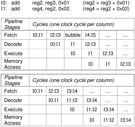
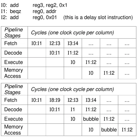
In the single issue processor true dependencies exist only between two consecutive instructions in different pipeline stages. Forwarding the result from the execution stage to the decode stage resolves the dependency and avoids stalling the pipeline. In a dual issue processor, true-dependencies can potentially exist between two parallel instructions. In this case, the pipeline has to be stalled for at least one clock cycle until the first instruction executes and its result is forwarded to the next instruction. Figure 13 shows an example of true-dependency between two parallel instructions. Although, instruction fetching is halted for a single cycle, in the next two consecutive cycles only a single instruction is issued which reduces the IPC by half during these two cycles.
The solution shown in Figure 13 (bottom) is to issue instruction I2 in parallel with I1 to fill up the empty fetch slot and maintain the flow of instructions coming to the decoder. In the following cycle, I3 is moved to the first slot and a new instruction I4 is fetched from program memory to fill one of the empty instruction slots. This process is equivalent to sliding instructions by a single slot which can be easily achieved by incrementing the program counter by one instruction instead of the usual two instructions. The advantage of this solution is that we can reuse the exact same circuit that detects true-dependency and slides instructions between different decoder slots to process control instructions (see next section for details). With this technique, only a single instruction slot is wasted instead of two instruction slots (see Figure 13) which results in a 50% reduction in wasted instruction slots per true-dependency.
I0: add reg2, reg3, 0x01 (reg2 = reg3 + 0x01)
I1: add reg4, reg2, 0x02 (reg4 = reg2 + 0x02)
Pipeline
Stages Cycles (one clock cycle per column)
Fetch I0:I1 I2:I3 bubble I4:I5 … …
Decode I0:I1 I1 I2:I3 … …
Execute I0 I1 I2:I3 … Memory
Access I0 I1 I2:I3
Pipeline
Stages Cycles (one clock cycle per column)
Fetch I0:I1 I2:I3 I3:I4 … … …
Decode I0:I1 I1:I2 I3:I4 … …
Execute I0 I1:I2 I3:I4 … Memory
Access I0 I1:I2 I3:I4
Figure 13. Example (top) of a true dependency between instructions within the same cycle and (bottom) a proposed solution to reduce the number of wasted instruction slots.
4.3. Branch Misprediction
Recovering from a mispredicted branch outcome is a difficult task in a dual issue pipeline because a branch instruction can be in any of the two available instruction slots. The calculation of the recovery address as well as the selection of instructions to be flushed out from the pipeline depends on which instruction slot in the decoder the branch instruction occupies. A simple solution is to decode the branch instruction only when it is located in the first decoder slot which guarantees that the instruction in the second slot is always going to be the delay slot instruction. When a branch instruction is detected in the decoder second slot, an exception is triggered which halts the issue of the branch instruction.
Although the branch instruction issue is delayed for one clock cycle, the branch target instruction is still fetched unless the branch delay slot instruction is not present in the fetch unit because of a previous branch instruction. In that case the delay slot instruction is fetched first. In the following cycle, the branch instruction is moved to the first slot and issued together with the delay slot instruction. The technique used to align branches to the first instruction slot is identical to the technique used to resolve true-dependency between instructions which consists of sliding instructions over by one slot. As a result, the true-dependency stall resolution logic can be reused as is to align branches to the first decoder slot with some minor additional logic for detecting branch instructions when they are present in the decoder second slot.
In some cases the delay slot instruction is not present in the fetch unit and has to be explicitly fetched which occurs when a branch instruction is decoded in the previous cycle and the target address of that branch instruction is loaded into the fetch unit instead of the current branch delay slot instruction (Figure 14 bottom). The issuing of the branch instruction as well as the fetching of the branch target address are delayed for an additional cycle until the delay slot instruction is fetched and loaded into the decoder unit. This process introduces a single bubble (empty slots) in the pipeline which cannot be avoided. Our simulation showed that the percentage of times that a delay slot instruction is not present in the fetch unit when a branch is detected in the decoder is less than 15% on average for the MiBench benchmark programs which is relatively low.
The decision to delay the issue of branch instructions until they are located in the first decoder slot wastes only a single decoder slot and only when the delay slot instruction I2 is present in the fetch unit as shown in Figure 14. Otherwise, if the delay slot instruction I2 is not present in the fetch unit (Figure 14 bottom example) then both approaches, i.e. issue branch instructions from the second decoder slot or delay branch instructions until they are moved to the first slot, have the same performance because the branch instruction is delayed anyway until the delay slot instruction is fetched regardless of which decoder slot the branch is located in.
and Intelligent Systems 09 2015 -01 2016 | Volume
3 | Issue 6 | e4
EAI
European Alliancefor Innovation 12
I0: add reg3, reg2, 0x1
I1: beqz reg0, addr
I2: add reg0, 0x01 (this is a delay slot instruction)
Pipeline
Stages Cycles (one clock cycle per column) Fetch I0:I1 I2:I3 I3:I4 … … …
Decode I0:I1 I1:I2 … … …
Execute I0 I1:I2 … … Memory
Access I0 I1:I2 …
Pipeline
Stages Cycles (one clock cycle per column) Fetch I0:I1 I8:I9 I2:I3 I3:I4 … …
Decode I0:I1 I1 I1:I2 … …
Execute I0 bubble I1:I2 … Memory
Access I0 bubble I1:I2
Figure 14. Example of a branch instruction located in the second slot and the corresponding delay slot instruction I2 (top) present and (bottom) not present in the fetch unit.
Using the above described technique to align branches to the first decoder slot and load the delay slot instruction into the second decoder slot guarantees that the effects of predicting or mispredicting a branch outcome will be equivalent as shown in Figure 15. The result in both cases is a single bubble or just two wasted instruction slots per branch instruction. Processors that don’t have a delay slot instruction such as the ARM Cortex can issue branch instructions directly from the second decoder slot.
I0: beqz reg0, In // If (reg0==0) then branch to In I2: add reg0, 0x01 // this is a delay slot instruction
Pipeline
Stages Cycles (one clock cycle per column) Fetch I0:I1 I2:I3 In:In+1 … … …
Decode I0:I1 I2:I3 In:In+1 … …
Execute I0:I1 bubble In:In+1 …
Memory
Access I0:I1 bubble In:In+1
Pipeline
Stages Cycles (one clock cycle per column) Fetch I0:I1 I2:I3 In:In+1 I4:I5 … …
Decode I0:I1 I2:I3 bubble … …
Execute I0:I1 I2:I3 bubble … Memory
Access I0:I1 I2:I3 bubble
Figure 15. Example of (top) a correctly predicted and (bottom) a mispredicted branch instruction.
4.4. Duplication of Resources
ALU
Processing two instructions per cycle requires that all the processor resources be duplicated, including the ALU. However, duplicating all the functions in the ALU will increase the total number of LE dramatically. Considering that the ALU uses 60% of the processor total LE and consumes 42% of total power, therefore adding two complete ALUs will increase power consumption by 2x.
We know from previous instruction distribution analysis that some of the operations appear very infrequently in the benchmarks like for example the multiplication instructions; adding an additional multiplier will have minimal impact on performance and increase power consumption unnecessarily. The dynamic power supplied to the additional multiplier can be either toned down using a variable clock [27] or turned off completely using clock gating [28] but it will hurt performance because it takes at least several cycles to restore the clock to its full speed. Static power consumption is even more difficult to switch off because it requires complex layout modifications to isolate each multiplier [29] and the response time of dc-to-dc voltage regulators is very slow [30] which preclude using these techniques in an embedded processor with a short pipeline. The only alternative is to reduce the number of duplicated resources to a minimum in order to minimize the increase in power consumption.
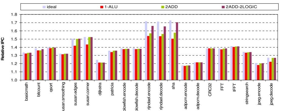
In order to determine which ALU resources are the most critical to performance, we conducted a thorough quantitative analysis for all benchmarks by selectively duplicating one ALU resource at a time and comparing the IPC results to the results of a dual issue processor with a single ALU (1-ALU Figure 16) to verify if there is any measurable improvement in performance. Results are summarized in Figure 16 and discussed in section 5.
Memories
A simple way to fetch two 32-bit instructions in parallel is to increase the program bus width from 32 bits to 64 bits. This simple scheme will work as long as we always fetch two consecutive instructions from memory. On the other hand, data accesses are not necessarily aligned which means that separate address and separate read/write ports are needed for each datum. In a dual issue processor, data memory needs to support two reads and two writes simultaneously which adds up to four read/write ports. Using any the methods evaluated for the RF implementation would be unfeasible because data memories are much larger than RFs; for example in our processor we use 32 Kbytes of data RAM. We measured the percentage of cycles during which two data memory accesses are issued in parallel using the compiler default settings and found it to be less than 3% on average for the MiBench programs. Therefore, we modified the GNU compiler to enforce mutual exclusivity between memory operations for the dual issue processor.
and Intelligent Systems 09 2015 -01 2016 | Volume
3 | Issue 6 | e4
EAI
European Alliancefor Innovation 13
1.0 1.1 1.2 1.3 1.4 1.5 1.6 1.7 1.8 b a s ic m a th b itc o u n t q s o rt s u s a n .s m o o th in g s u s a n .e d g e s s u s a n .c o rn e r d ijk s tr a p a tr ic ia b lo w fis h .e n c o d e b lo w fis h .d e c o d e ri jn d a e l. e n c o d e ri jn d a e l.d e c o d e s h a a d p c m .e n c o d e a d p c m .d e c o d e C R C 3 2 F F T IF F T s tr in g s e a rc h jp e g .e n c o d e jp e g .d e c o d e R e la ti v e I P C
ideal 1-ALU 2ADD 2ADD-2LOGIC
Figure 16. IPC results for a dual issue processor relative to the IPC of a single issue processor using a static branch predictor with an always taken heuristic under different ALU configurations. The ideal case is for a processor with two complete ALU units.
5. Results
5.1. Simulation
Simulation results for the dual issue processor are summarized in Figure 16. These results include the duplication of resources evaluation discussed in section 4.3. The main observations are:
Dual Issue
• The average increase in IPC for a dual issue processor is around 40%. Some benchmarks like rijndael and sha experienced an approximately 1.6x improvement in IPC. Because the dual issue processor lacks advanced superscalar techniques to issue instructions out-of-order it can only extract parallelism from within basic blocks boundaries which favours benchmarks with longer basic blocks like rijndael and sha. On the other hand, the worst performing benchmark, adpcm, still managed to achieve at least a 20% gain in IPC. Benchmarks with a high percentage of control instructions like adpcm might benefit from using a dynamic branch predictor combined with out-of-order issue to increase the prediction success rate. Figure 7 results show that adpcm (telecom group) IPC increased by 5% when a bimodal branch predictor was used.
• The next best performing benchmarks are susan.edges and susan.corner which experienced a 1.5x speedup. These benchmarks have a much higher percentage of memory operations than the rijndael and sha benchmarks but share the common characteristic of low control operations. A low percentage of control operations translate to less interruption to the pipeline and consequently shorter overall program latency.
• Despite the low percentage of control operations in the susan.smoothing benchmark, it did not perform as well as the other susan benchmarks because the high percentage of IMUL operations increased the percentage of true-dependencies between the multiplication operations and the REGMOV operations that loads the result of the multiplication into the RF.
• One benchmark program that did not perform as good as expected is jpeg. Although the jpeg benchmark is a compression and decompression application similar to rijndael, it performed much worse than rijndael. The reason is that the length of basic block in the rijndael benchmarks is almost 2x longer than in the jpeg benchmarks, which translates to higher ILP and better speedup.
• Using just an advanced branch predictor is not enough to improve jpeg IPC results as Figure 7 results show (the consumer group IPC only improved by 2%). Out-of-order issue is mandatory in order to fetch and issue instructions beyond the jpeg basic block boundaries.
• The amount of ILP in a basic block that can be extracted by the processor using available hardware resources is a key factor for improving performance.
Resource Duplication
• The ideal case results in Figure 16 are for a dual issue processor with two complete ALU units. Considering that the ALU uses 60% of the processor total LE and consumes 42% of the processor total power budget, it would be unfeasible to implement it in hardware. However, we include these results for comparison reasons only. For example, most benchmarks approached ideal performance with just minor resource duplications.
and Intelligent Systems 09 2015 -01 2016 | Volume 3 | Issue 6 | e4
EAI
European Alliancefor Innovation 14
• The average drop in IPC for a single ALU configuration is around 2% which is negligible. Few benchmarks like susan, adpcm.encode and jpeg.decode experienced an IPC loss higher than 5%. Although the IPC loss is higher than the average it is still acceptable considering that the total gain in IPC is higher than 10%. In the case of the susan benchmarks the gain in IPC is almost 1.5x. Increasing the number of adders to two helped these benchmarks recover all the lost performance. • Only the rijndael benchmarks experienced a loss in
IPC from using a single logic unit. Adding a second logic unit to the ALU managed to recover just half the lost IPC. The remaining lost IPC is tied to the other ALU functions such as logic shifts.
5.2. FPGA Implementation
Table 5 compares the FPGA implementation results of the dual issue processor with the results of the single issue processor listed in Table 4. The main observations are:
• The max speed of the dual issue processor is the same as the single issue processor because it is determined by the speed of the worst case path which goes through the 32-bit multiplier.
• The total number of FPGA logical elements increased by approximately 30% (Figure 17), from 1.8K to 2.3K which is less than 10% of the FPGA total resources. The biggest increase was in the RF which grew from 87 LE (5% of total LEs) to 494 LE (22% of total LEs).
• The total number of RAM bits used by the RF quadrupled from 2-Kbits to 8-Kbits using our proposed 1-bit tagging method.
• Power consumption increased by 20% (Figure 18), from 0.48 mWatts/MHz to 0.57 mWatts/MHz. The RF power consumption as a percentage of total power is much higher in the dual issue processor, 56% compared to 28%, which makes it the dominant power consuming module in the processor. The ALU power consumption went down to less than 30% total power because we only added an extra 32-bit adder. • The Coremark/MHz performance increased by
almost 36% compared to the single issue processor. The 3.40 Coremark/MHz score is equal to MicroAptive and Cortex-M4 Coremark/MHz scores. The reason that the MicroAptive and Cortex-M4 single issue processors can achieve such as high score is because they use advanced commercial compilers, such as Green Hills (http://www.ghs.com) and IAR (http://www.iar.com), to fine tune and optimize the benchmark code for the specific processor architecture [31]. In our case we use the open source GNU compiler which although can achieve very good performance it consistently delivered lower Coremark results than commercial compilers [7].
Table 5. Summary of FPGA resource utilization for the dual issue processor with a single ALU.
Resource Single Issue Dual Issue
Logic elements 1,831 2,278 Logic RAM (bits) 2K 8K Physical RAM
block (M9K) 2 8
Embedded 9-bit
multipliers 8 8
Speed (MHz) 60 60
Dynamic power
(mWatt/MHz) 0.48 0.57 Coremark/MHz 2.51 3.40
Decoder 15%
ALU 51% Connectivity
12% Register
File 22%
Figure 17. Percentage of processor logic cells per module for dual issue processor.
Decoder 13% Register
File 56%
Connectivity 6%
ALU 25%
Figure 18. Percentage of total processor power per module for standalone dual issue core.
6. Conclusion
A single issue scalar processor can operate on a very low power budget but its performance is constrained. On the other hand, a multi-issue superscalar processor can deliver multiple fold increase in performance but is power intensive. To address this problem, a dual issue scalar processor capable of processing up to two instructions simultaneously every cycle is introduced. The processor delivers an average 40% higher IPC than a single issue processor while consuming only 20% more power. Applications that contain a large amount of instruction-level parallelism are particularly suitable for the dual issue processor and experience up to 70% improvement in IPC. The dual issue processor is implemented on a low cost FPGA using less than 10% of the total logic elements which leaves plenty of resources to implement additional functions. The proposed processor is an ideal candidate for embedded industrial devices that are powered by green sources of energy similar to PowerFilm embedded solar panels.
and Intelligent Systems 09 2015 -01 2016 | Volume
3 | Issue 6 | e4