www.ijiarec.com
Volume-5 Issue-1
International Journal of Intellectual Advancements
and Research in Engineering Computations
Efficient error detection codes for multi code upset correction in
SRAM based FPGA
Sangavi S
1, Sathya Prabha R
2, Nandha Kumar A
3, Shiva shanmugam K M
4, Maheswari T
51,2,3,4
UG Student, Department of ECE, Nandha Engineering College, Erode
5
Asst. Professor, Department of ECE, Nandha Engineering College, Erode
[email protected]
Abstract— Multiple cell upsets (MCUs) are fetching major issues in the dependability of memories out in the open to radiation atmosphere. To stop MCUs from cause data corruption, more complex error correction codes (ECCs) are widely used to protect memory, but the main problem is higher delay overhead. In this paper, novel decimal matrix code (DMC) based on divide-symbol is projected to boost memory reliability with lower delay overhead. The proposed DMC utilizes decimal algorithm to obtain the maximum error detection capability. Moreover, the encoder-reuse technique (ERT) is proposed to minimize the area overhead of extra circuits. ERT uses DMC encoder itself to be part of the decoder. Occurrence of such errors in the configuration frames of a field-programmable gate array (FPGA) device permanently affects the functionality of the mapped design. In this paper, we present a low-cost error-detection code to detect MBUs in configuration frames as well as a generic scrubbing scheme to reconstruct the erroneous configuration frame based on the concept of erasure codes. The proposed scheme does not require any modification to the FPGA architecture. Implementation of the proposed scheme on a Xilinx Virtex-6 FPGA device shows that the proposed scheme can detect 100% of MCUs in the configuration frames with only 3.3% resource occupation, while the recovery time is comparable with the previous schemes.
I. INTRODUCTION
CMOS technology scales down to nanoscale and memories are combined with an increasing number of electronic systems, the soft error rate in memory cells is rapidly increasing, especially when memories operate in space environment due to ionizing effect atmospheric neutron, alpha-particle, and cosmic rays
Although single bit upset is a major concern about memory reliability, multiple cell upsets (MCUs) have become a serious reliability concern in some memory applications. In order to make memory cells as fault-tolerant as possible, some error correction codes (ECCs) have been widely used to protect memories against soft errors for years. For example, the Bose–Chaudhuri– Hocquenghem codes, Reed–Solomon codes, and punctured difference set (PDS) codes have been used to deal with MCUs in memories. But these codes require more area, power, and delay overheads since the encoding and decoding circuits are more complex in these complicated codes.
Interleaving technique has been used to restrain MCUs which rearrange cells in the physical arrangement to separate the bits in the same logical word into different physical words. However, interleaving technique may not be practically used in content-addressable memory (CAM), because of the tight coupling of
hardware structures from both cells and comparison circuit structures
Built-in current sensors (BICS) are proposed to assist with single-error correction and double-error detection codes to provide protection against MCUs . However, this technique can only correct two errors in a word.
More recently, in , 2-D matrix codes (MCs) are proposed to efficiently correct MCUs per word with a low decoding delay, in which one word is divided into multiple rows and multiple columns in logical. The bits per row are protected by Hamming code, while parity code is added in each column. For the MC based on Hamming, when two errors are detected by Hamming, the vertical syndrome bits are activated so that these two errors can be corrected. As a result, MC is capable of correcting only two errors in all cases. In , an approach that combines decimal algorithm with Hamming code has been conceived to be applied at software level. It uses addition of integer values to detect and correct soft errors. The results obtained have shown that this approach have a lower delay overhead over other codes.
Fig 1. Main Block Diagram
In this paper, novel decimal matrix code (DMC) based on divide-symbol is proposed to provide enhanced memory reliability. The proposed DMC utilizes decimal algorithm (decimal integer addition and decimal integer subtraction) to detect errors. The advantage of using decimal algorithm is that the error detection capability is maximized so that the reliability of memory is enhanced[1]. Besides, the encoder-reuse technique
334
(ERT) is proposed to minimize the area overhead of extra circuits (encoder and decoder) without disturbing the whole encoding and decoding processes, because ERT uses DMC encoder itself to be part of the decoder
SRAM-BASED field-programmable gate arrays (FPGAs) are widely used in a variety of application domains due to short time-to-market time, flexibility, high density, and cost-efficiency[15]. However, increasing transistor count per chip (i.e., Moore’s law) coupled with the reduced operating voltage in the past years results in an exponential growth in soft error rate (SER) of digital circuits. Considering the proliferation of FPGAs in a variety of safety- and mission-critical applications, it is crucial to mitigate their susceptibility to these kinds of errors .
In order to meet the ever-increasing performance and power demands, FPGAs are typically fabricated using the most advanced technology nodes. Recently, FPGAs based on a 14-nm technology with denser integration schemes, such as 3-D die stacking, have been announced. In such small device geometries, a single radiation-induced particle strike is likely to affect several adjacent cells in a memory array, leading to a multiple bit upset (MBU) . Considering the fact that the MBU rate in nano scales is comparable with the single event upset (SEU) an appropriate schemes required to detect and correct multiple errors in memory arrays. More specifically, SRAM-based FPGAs are more prone to soft errors as a particle strikes in a configuration frame has a permanent impact on the functionality of the mapped design. Since the configuration frames constitute the majority of SRAMs in an FPGA device (e.g., >80% for Xilinx Virtex-6 VLX240T), mitigation of MBUs in configuration frames is of decisive importance.
Several schemes have been presented to address the increasing soft error concern in the FPGA configuration frames. The main objective of these schemes is to reduce error latency, and hence, to avoid error accumulation within configuration frames. Costly modular redundancy is a conventional technique to tolerate soft errors in both configuration frames and functional logic. However, accumulated errors in both data and configuration bits dramatically limit the mean time to failure of such schemes. Another technique is to optimize the configuration frame circuitry for soft errors as detailed[16]. However, such hardening techniques are not implemented in the existing FPGA devices because of their excessive area overheads. Therefore, a low-cost solution is required to correct erroneous configuration frames during operation. The combination of configuration scrubbing and error correction codes (ECCs) is an effective solution to detect and correct radiation-induced transient errors in configuration bits. In this regard, an SEU tolerant scrubbing scheme is very well studied in the literature, and it is already included in Xilinx and Altera design flows.
There are also a few schemes to specifically address MBUs in FPGA devices. In addition, Xilinx offers a soft error mitigation controller (IP block) based on cyclic redundancy code (CRC) and ECC which can correct up to two adjacent erroneous cells in each configuration frame[17]. Recent experiments reveal that the number of affected bits by an MBU incident grows as technology scales. Once an error is detected, by taking advantage of erasure codes and using the data stored in a redundant frame, the correct contents of the affected configuration frame are reconstructed. Furthermore, by carefully dividing the frames into several
clusters, the proposed technique can detect and correct an MBU affecting several adjacent configuration frames.For the case study on a Xilinx FPGA device, the proposed parity technique is able to detect 100% of the soft errors, and all detected errors are successfully recovered by means of DMC codes.
II.PROPOSED DMC:
In this section, DMC is proposed to assure reliability in the presence of MCUs with reduced performance overheads, and 32-bit word is encoded and decoded as an example based on the proposed techniques.
III. PROPOSED SCHEMATIC OF
FAULT-TOLERANT MEMORY
First, during the encoding (write) process, information bits D are fed to the DMC encoder, and then the horizontal redundant bits H and vertical redundant bits are obtained from the DMC encoder. When the encoding process is completed, the obtained DMC codeword is stored in the memory. If MCUs occur in the memory, these errors can be corrected in the decoding (read) process. Due to the advantage of decimal algorithm, the proposed DMC has higher fault-tolerant capability with lower performance overheads. In the fault-tolerant memory, the ERT technique is proposed to reduce the area overhead of extra circuits and will be introduced in the following sections.
IV. PROPOSED DMC ENCODER
In the proposed DMC, first, the divide-symbol and arrange-matrix ideas are performed, i.e., the N -bit word is divided into k symbols of m bits (N = k × m), and these symbols are arranged in a k1 × k2 2-D matrix (k = k1 × k2, where the values of k1 and k2 represent the numbers of rows and columns in the logical matrix respectively). Second, the horizontal redundant bits H are produced by performing decimal integer addition of selected symbols per row. Here, each symbol is regarded as a decimal integer. Third, the vertical redundant bits V are obtained by binary operation among the bits per column. It should be noted that both divide-symbol and arrange-matrix are implemented in logical instead of in physical. Therefore, the proposed DMC does not require changing the physical structure of the memory.
To explain the proposed DMC scheme, we take a 32-bit word as an example, as shown in Fig. 2. The cells from D0 to D31 are information bits. This 32-bit word has been divided into eight symbols of 4-bit. k1 = 2 and k2 = 4 have been chosen simultaneously. H0–H19 are horizontal check bits;
3-bit errors can be corrected and the number of redundant bits is reduced to 32. However, when k = 2 × 4 and m = 4, the maximum correction capability is up to 5 bits and the number of redundant bits is 36. In this paper, in order to enhance the reliability of memory, the error correction capability is first considered, so k = 2 × 4 and m = 4 are utilized to construct DMC.
The horizontal redundant bits H can be obtained by decimal integer addition as follows:
335
and similarly for the horizontal redundant bits H14H113H12H11H10 and H19H18H17H16H15 where “+” represents decimal integer addition.
For the vertical redundant bits V , we have
V0 = D0⊕ D16 (3)
V1 = D1⊕ D17 (4)
and similarly for the rest vertical redundant bits.
Fig. 2 32 bit DMC Encoder using multi bit adder and Ex or gates.
The encoding can be performed by decimal and binary addition operations. The encoder that computes the redundant bits using multi bit adders and XOR gates is shown in Fig. 3. In this figure, H19 − H0 are horizontal redundant bits, V15 − V0 are vertical redundant bits, and the remaining bits U31 − U0 are the information bits which are directly copied from D31 to D0. The enable signal E n will be explained in the next section.
V. PROPOSED DMC DECODER:
To obtain a word being corrected, the decoding process is required. For example, first, the received redundant bits H4 H3 H2 H1 H0 and V0 − V3 are generated by the received information bits D. Second, the horizontal syndrome bitsH4 H3 H2 H1 H0 and the vertical syndrome bits S3 − S0 can be calculated as follows:
H4 H3 H2 H1 H0 = H4 H3 H2 H1 H0 − H4 H3 H2 H1 H0 (5)
S0 = V0⊕ V0 (6)
and similarly for the rest vertical syndrome bits, where “−” represents decimal integer subtraction.
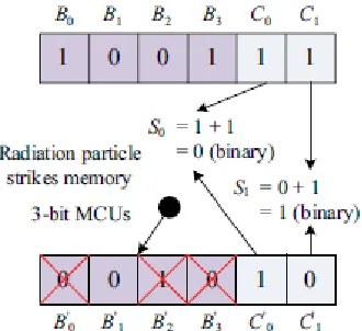
When H4 H3 H2 H1 H0 and S3 − S0 are equal to zero, the stored codeword has original information bits in symbol 0 where no errors occur. When H4 H3 H2 H1 H0 and S3 − S0 are nonzero, the induced errors (the number of errors is 4 in
Fig 3. Representation of the data bits
D
0correct = D0 ⊕S0. (7) The proposed DMC decoder is depicted in Fig. 4, which is made up of the following submodules, and each executes a specific task in the decoding process: syndrome calculator, error locator, and error corrector. It can be observed from this figure
that the redundant bits must be recomputed from the received information bits D and compared to the original
Fig 4. Limits of binary error detection in simple binary operations.
Set of redundant bits in order to obtain the syndrome bits H and S. Then error locator uses H and S to detect and locate which bits some errors occur in. Finally, in the error corrector, these errors can be corrected by inverting the values of error bits.In the proposed scheme, the circuit area of DMC is minimized by reusing its encoder. This is called the ERT. The ERT can reduce the area overhead of DMC without disturbing the whole encoding and decoding processes. From Fig. 4, it can be observed that the DMC encoder is also reused for obtaining the syndrome bits in DMC decoder. Therefore, the whole circuit area of DMC can be minimized as a result of using the existent circuits of encoder. Besides, this figure also shows the proposed decoder with an enable signal E n for deciding whether the encoder needs to be a part of the decoder. In other words, the E n signal is used for distinguishing the encoder from the decoder, and it is under the control of the write and read signals in memory. Therefore, in the encoding (write) process, the DMC encoder is only an encoder to execute the encoding operations. However, in the decoding (read) process, this encoder is employed for computing the syndrome bits in the decoder. These clearly show how the area overhead of extra circuits can be substantially reduced
Fig 5. Block diagram for encoder and decoder.
VI. LIMITS OF SIMPLE BINARY ERROR DETECTION:
336
bits and the bits C0 and C1 are redundant bits. The bits C0 and C1 are obtained using the binary algorithm
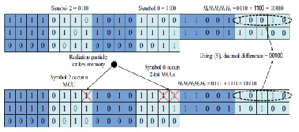
Fig 6. Advantage of decimal error detection. Using decimal algorithm H4H3H2H1H0 Will not be 0 decimal. This representation helps to reduce the error.
This code has the least β value but its correction capability is a constant (1). For the MC [11], its correction capability is also a constant (2) due to the limits of error correction capability of hamming code. PDS [6] has a lower β value compared with the proposed scheme, but it requires higher delay overhead which would severely affect the access time of memory. The scaling down of CMOS technology has resulted in a dramatic increase in the number of MCUs. In 90-nm technology, more than three errors have been observed in radiation test [1], [2], [12], [13], so Hamming, MC, and PDS are not good choices for protecting memory. The proposed scheme needs higher β value than other codes but it has higher correction capability. Therefore, designers should choose the optimal combination of k and m based on the radiation test to provide a good trade off between reliability and redundant bits. Fig. 6 shows the values of this metric for different protection codes. From this figure, we can see that the proposed scheme has a higher CCC value than other codes except that only one MCU occurs. Therefore, based on the results and Fig. 7, the proposed scheme is quite suitable for high-speed memory applications[7]. It should be mentioned that when the number of errors is more than two
Symbol 3 Symbol 2 Symbol 1 Symbol 0 H
m = 8
Fig. 7. Proposed fault-tolerant CAM using decimal error detection
technique together with BICS.
Note that when errors do not exist in CAM, the stored codeword is directly output without though error detection and correction circuits. (b) 32-bit word organization in CAM (k = 1 × 4 and m = 8)per word, Hamming and MC [11] codes cannot correct any errors.
VII. DECIMAL ERROR DETECTION IN SRAM
ECC code is a very powerful technique to correct MCUs in memory, as mentioned before. However, ECC implementation in CAM is significantly different from its implementation in SRAM due to simultaneous access to all the words in CAM, so that ECC code is not suitable to directly protect CAM [8]. In [10], BICS together with Hamming code is used to protect SRAM. Because BICS has zero fault-detection latency for multiple error detection, it is suitable for detection errors in CAM as well.
For the decimal error detection, this ability to detect any type of error can be useful in CAM. Let us consider that the decimal error detection technique combines with BICS to protect CAM. The fault-tolerant CAM structure is depicted in Fig. 8 and a 32-bit word organization in CAM is proposed in Fig. 8. For each column of CAM, BICS is added to detect the error (the basic principle and circuit of BICS are shown in [9] and [10]).
VIII. IMPLEMENTATION ON A XILINX FPGA DEVICE
As a proof of concept, we implemented the proposed technique on a Xilinx Virtex-6 VLX240T device. In this section, we explain the implementation flow validated by a fault injection experiment[14]. Then, we discuss the recovery time and area overhead trade off in detail and quantitatively compare the proposed scheme with the existing solutions.
A. IMPLEMENTATION FLOW
Xilinx FPGAs offer several interfaces to read and modify the configuration frames [18]. Internal configuration access port (ICAP) is one of the fastest interfaces which operates at the frequency of 100 MHz. In this paper, this interface has been used as it is within the FPGA fabric and could be controlled by a custom hardware block.
We wrote a reconfigurable implementation of the EDR unit in Verilog which accepts the overall number of frames and the number of clusters as input. This implementation is completely independent of the user design and needs to be merged with the latter before mapping into the FPGA device.
Fig. 8. Implementation flow of the proposed scheme to a Xilinx FPGA device.
337
configuration frame. Then, the updated bit stream is programmed into the FPGA.
B. VALDIATION WITH FAULT INJECTION
In order to validate the EDR capabilities of the proposed technique, we performed a fault injection experiment on the configuration bits of the Xilinx Virtex-6 VLX240T device. The fault injection is done by reading a randomly selected configuration frame using the ICAP interface. Afterward, a random MBUP is applied to a random location of the frame and eventually the modified contents are written back to the configuration frame using the same interface. We have injected 1000 errors on the configuration frames and initiated one iteration of scrubbing[19]. At the end of the scrubbing period, we read the contents of the erroneous frame and compared its contents with the golden state before fault injection. The experimental result shows that the proposed technique is able to detect and correct all injected errors.
C. AREA AND POWER OVERAHEAD
In the employed Xilinx Virtex-6 XLV240T device, there are 28 464 configuration frames each of which comprising of 81 32-bit words. In addition, each configuration frame has 16 spare bits for the Xilinx SEU correction mechanism .The parity requires 10 bits to reach its maximum detection coverage (i.e., 100%) and these
bits could be stored in these 16 spare bits of the corresponding frame without any other storage mechanism such as SRAMs. Please note that the complete 3-D parity scheme requires 2 × (81 + 32) = 226 bits for each configuration frame which has to be stored in a SRAM unit.
D. CONCLUSION:
In this paper, novel per-word DMC was proposed to assure the reliability of memory. The proposed protection code utilized decimal algorithm to detect errors, so that more errors were detected and corrected. The obtained results showed that the proposed scheme has a superior protection level against large MCUs in memory. Besides, the proposed decimal error detection technique is an attractive opinion to detect MCUs in CAM because it can be combined with BICS to provide an adequate level of immunity.
The only drawback of the proposed DMC is that more redundant bits are required to maintain higher reliability of memory, so that a reasonable combination of k and m should be chosen to maximize memory reliability and minimize the number of redundant bits based on sradiation experiments in actual implementation.
REFERENCES:
1. D. Radaelli, H. Puchner, S. Wong, and S. Daniel, “Investigation of multi-bit upsets in a 150 nm technology SRAM device,” IEEE Trans. Nucl. Sci., vol. 52, no. 6, pp. 2433–2437, Dec. 2005.
2. E. Ibe, H. Taniguchi, Y. Yahagi, K. Shimbo, and T. Toba, “Impact of scaling on neutron induced soft error in SRAMs from an 250 nm to a 22 nm design rule,” IEEE Trans. Electron Devices, vol. 57, no. 7, pp. 1527–1538, Jul. 2010.
3. C. Argyrides and D. K. Pradhan, “Improved decoding algorithm for high reliable reed muller coding,” in Proc. IEEE Int. Syst. On Chip Conf., Sep. 2007, pp. 95–98.
4. Sanchez-Macian, P. Reviriego, and J. A. Maestro, “Hamming SEC-DAED and extended hamming SEC-DED-TAED codes through selective shortening and bit placement,” IEEE Trans. Device Mater. Rel., to be published.
5. S. Liu, P. Reviriego, and J. A. Maestro, “Efficient majority logic fault detection with difference-set codes for memory applications,” IEEE Trans. Very Large Scale Integr. (VLSI) Syst., vol. 20, no. 1, pp. 148–156, Jan. 2012..
6. P. Reviriego, M. Flanagan, and J. A. Maestro, “A (64,45) triple error correction code for memory applications,” IEEE Trans. Device Mater. Rel., vol. 12, no. 1, pp. 101–106, Mar. 2012.
7. K. Pagiamtzis and A. Sheikholeslami, “Content addressable memory (CAM) circuits and architectures: A tutorial and survey,” IEEE J. Solid-State Circuits, vol. 41, no. 3, pp. 712– 727, Mar. 2003.
8. S. Baeg, S. Wen, and R. Wong, “Minimizing soft errors in TCAM devices: A probabilistic approach to determining scrubbing intervals,”
9. IEEE Trans. Circuits Syst. I, Reg. Papers, vol. 57, no. 4, pp. 814–822, Apr. 2010.
10. P. Reviriego and J. A. Maestro, “Efficient error detection codes for multiple-bit upset correction in SRAMs with BICS,” ACM Trans. Design Autom. Electron. Syst., vol. 14, no. 1, pp. 18:1–18:10, Jan. 2009.
11. C. Argyrides, R. Chipana, F. Vargas, and D. K. Pradhan, “Reliability analysis of H-tree random access memories implemented with built in current sensors and parity codes for multiple bit upset correction,” IEEE Trans. Rel., vol. 60, no. 3, pp. 528–537, Sep. 2011.
12. C. Argyrides, D. K. Pradhan, and T. Kocak, “Matrix codes for reliable and cost efficient memory chips,” IEEE Trans. Very Large Scale Integr. (VLSI) Syst., vol. 19, no. 3, pp. 420–428, Mar. 2011.
338
14. N. N. Mahatme, B. L. Bhuva, Y. P. Fang, and A. S. Oates, “Impact of strained-Si PMOS transistors on SRAM soft error
rates,” IEEE Trans. Nucl. Sci., vol. 59, no. 4, pp. 845–850, Aug. 2012.
15. Dixit and A. Wood, “The impact of new technology on soft error rates,” in Proc. IEEE Int. Rel. Phys. Symp. (IRPS), Apr. 2011,5B.4.1–5B.4.7.
16. C. Hu and S. Zain, “NSEU mitigation in avionics applications,” Xilinx Corporation, San Jose, CA, USA, Appl. Note XAPP1073, 2011,
17.1–12.
18. P. Dorsey, “Xilinx stacked silicon interconnect technology delivers breakthrough FPGA capacity,
bandwidth, and power efficiency,” Xilinx Corporation, San Jose, CA, USA, White Paper Virtex-7 FPGAs, 2010, pp. 1–10.
19. Altera Corporation, “Meeting the performance and power imperative of the zettabyte era with generation 10,” Altera Corporation, San Jose, CA, USA, White Paper WP-01200-1.0, 2013.