Volume-6 Issue-4
International Journal of Intellectual Advancements
and Research in Engineering Computations
Insertion of real time into small scale embedded design
1
Mr.N Ravindar,
2Mr.Sureshpalaka Dean,
3Ms.T Divya
Assistant Professor, ECE Department, HITS, Hyderabad. HIT IInd Shift Polytechnic College, Hyderabad. Assistant Professor, ECE Department, HITS, Hyderabad.
ABSTRACT
Microcontrollers play an important role in embedded system designs. Particularly, Small scale embedded designs which are developed using 8051 and its different versions involve effective designs with low cost. These controllers are having features like inbuilt memories, Timers, Serial control bus etc., but not real time features. To introduce real time features and make fast the serial communication interface among memories the proposed design introduced. The proposed work is the best solution for cost reduction by using low end microcontrollers where high end microcontrollers used.
Keywords: Microcontrollers, I2C, Master, Slave, Registers
INTRODUCTION
Serial bus requires fewer IC pins, and the less wiring and less number of traces on printed circuit boards than parallel bus. Many common embedded system peripherals support serial interfaces. Using I2C, processors do not require shared memory to communicate. I2C called as inter integrated circuit is a simple, low-bandwidth, short-distance protocol. It was made by Philips Semiconductors in the early 1980s reduce the manufacturing costs of electronic products. The I2C allows 7-bit or 10 bit addressing with two bi-directional lines: serial clock (SCL) and serial data (SDA). The pull-up resistors for each line are only added. All the devices on the line can act as either a slave or a master. The clock line can only be drive by the master devices. The transmission of 8-bit of data and 7-bit of address with a control bit is done serially using the interface.
It is difficult to verify the functionality of the design using traditional test benches as the design becomes large. Thus, hardware verification
which also consumes more resources than the design itself. This arise the need for developing modular, reusable and robust environment for verification. The Open Core Protocols (OCP) was introduced for accessing System on Chip functional units along with maintaining high performance. It allows software address communication between the units of Chip.
I2C PROTOCOL
I2C provides chip-to-chip serial communications using only two lines in an interface shown in figure.1. The two lines in the I2C bus carry one bit of address selection, direction control, and data at a time. The data (SDA) line carries the data, while the Clock (SCL) line synchronizes the sender and receiver during the transfer. Device that uses I2C protocol requires very few pins to perform the same function as their larger parallel interface equivalents. The I2C bus has three modes of operation: standard mode (0 to 100 kbps), fast mode (0 to 400 kbps) and
I2C Specifications
The I2C bus physically consists of two bidirectional active wires- serial Data line, serial Clock line and a ground connection. Each device connected to the bus has its own unique address and can act as a receiver or a transmitter, depending on the required functionality. The I2C bus is designed as a multi-master bus. The bus Master is the IC that starts a data transfer on the bus and all the other ICs are regarded as Slaves. Master will issue an 'Attention' signal to all of the connected devices known as START. Then the Master sends the ADDRESS of the slave device it
wants to access. The Read or Write operation signal bit is also send along with the ADDRESS bits. All the devices connected on the bus will compare the sent address bits with their own address and if it doesn't match, they simply wait till the bus is released and ifthe address matches; chip will produce a response signal known as Acknowledgement (ACK). On receiving an acknowledgement, master starts transmission of DATA. Each data byte is 8 bits long. An acknowledge bit follows each transferred byte. After transmission is done, the Master will issue the STOP signal
I2C COMMUNICATION FRAME FORMAT
WRITE OPERATION FRAME FORMAT
READ OPERATION FRAME FORMAT
START and STOP condition
All communication begins from a START signal and can be finished by a STOP signal. SCL being High and a high to Low transition on the
Fig 2: Start (S) and Stop (P) condition
Transfer Data and acknowledgement format
Every byte that is that is transferred using SDA line must be 8 bit long. Each transferred byte is
followed by an Acknowledge bit. Format is shown in figure 3.
Fig 3: Data and acknowledgement in I2C protocol
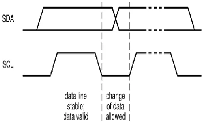
Data Validity
The data on the SDA line are valid for high period of serial clock pulse as shown in the figure 4 below.
Fig 4: Timings of data validation
Real Time Clock
A clock which keeps track the time even in device is off mode is called Real Time Clock. This clock is powered with unbroken battery even that
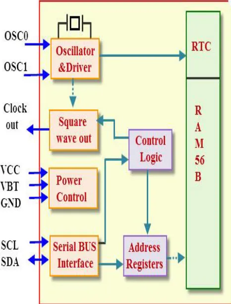
of RTCs interfaced to it. So here is a brief information regarding interfacing of RTC DS1307 device with 8051 microcontroller.
management in electronic designs were interfaced with external circuitry. The projects run with real time management is possible and Implemented for those designs. Now a proposal developed the RTC module run with I2C to reduce the fetch time across EEPROM memories. The implementation of RTC with I2C how interfaced with 8051.
PROCEDURE
The interfacing with 8051ofRTC and I2C are explained.
Step-1: Selection of RTC Device
There are different types of RTC (real time clock)devices are available in the embedded system marketand these are classified into different types like supply voltage, package type and pin diagram etc. A few kinds of RTC devices are;
2-Wire Serial Interface (or) I2C Bus
3-Wire Serial Interface (or) USB BUS
4-wire Serial interface (or) SPI BUS
First of all, we must select the type of device based on type like SPI bus RTC or I2C bus RTC, or any other device, which is apt for interfacing with a microcontroller. Then, choose the features of the RTC device depending on application like suitable package & clock frequency, battery life. Let us
to store the data and battery is for backup in case of power supply failure.
A0, A1 and A2 pins are address pins
VCC and GND pins are power supply (1.8V to 5.5V range) and ground pins.
VBT is a battery power supply (2V to 3.5V)
SCL pin is a serial clock and it is used to synchronize data on the serial interface.
SDL pin is a serial i/p and o/p pin.
CLK Out pin is an optional square wave o/p pin.
OSC0 & OSC1 pins are crystal oscillator pins
Addressing of the Device
The I2C bus protocol lets many dependent devices at a time. Every dependent device must comprise of own address to denote on it. The master device interconnects with a particular dependent device by an address. The address of the RTC device is OxA2 where 1010 is given by the manufacturer and, address pins A0, A1 and A2 are used to interconnect with eight RTC devices on the 2C bus protocol.
R/W bit is used to perform read or write operations in RTC. If R/W is equal to 0, write operation is performed and R/W is equal to 1, read operation is performed.
The address of the read operation of RTC is 0xA3
Figure.5 Configuration of RTC DS1307
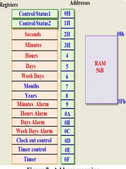
Figure 6. Address Registers Format
Address and Memory Registers
RTC registers are placed at 00h to 0Fh locations. RAM memory registers are also located at 08h to 3Fh locations. These registers are used to
Figure 7. Address mapping
Status/Control Registers
RTC DS1307 comprises of two extra registers like control or status register1 and control or status
register2. These registers are used to control RTC & Interrupts.
Control or Status Register1
TEST1=0 is the normal mode = w1 EXT is the clock test mode STOP=0 RTC starts =1
RTC stopTESTC=0
power on reset inactivated = power on reset activated
Step3: Interfacing RTC DS1307 Device with 8051 Microcontroller
RTC DS1307 can be interfaced with 8051 microcontroller using various serial bus protocols like SPI and I2C that provides a communication link between them. The circuit below shows RTC DS1307 interfacing with 8051 microcontroller using I2C bus protocol. It is a bi-directional serial protocol and it consists of 2-wires like SDA and SCL. These wires are used to transfer data between devices which are connected to the bus. The 8051 microcontroller doesn’t contain inbuilt RTC device.
So, we have connected externally via a serial communication for confirming the comprising data. I2C bus protocols have open drain o/ps so, a pull-up resistor is connected to the I2C bus line with a voltage source. If the resistors are not connected to the SDL and SCL lines, the I2C bus does not work.
Step4: Format of RTC Data Framing
I2C bus is used in the interfacing of RTC with a microcontroller. So, the data transfer is in the form of packets or bytes, and these are followed by a credit.
Figure.8 I2C Interfacing circuit with 8051
Data Transmitting Frame
In transmitting mode, after selecting a slave device by using address bit, the master device releases the start condition. The address bit includes seven bits that specify the slave devices as
Receiving Data Frame
7- Bit Address: Master sends the slave address into two 8-bit formats in the place of a single 16-bit address.
Control Status Register Address: This register address is mainly used to let the control status registers.
Control Status Register1: This register used to activate the RTC device
Control Status Register2: This register is used to enable & disable interrupts.
R/W: When read & write bit is high, then the read operation is performed.
Acknowledgement
When a write operation is performed on the slave device, then the microcontroller receives the 1-bit ACK from the receiver.
Stop: When write operation of the slave device is completed, then the microcontroller sends a stop condition to slave
CONCLUSION
The proposed work as interfacing with microcontrollers using design of RTC. The output with clock time and Supporting to enhance speed of data serial communication is successfully.
REFERENCES
[1]. Alexander W. Rath, Volkan Esen and Wolfgang Ecker. A Transaction-Oriented UVM-Based Library for Verification of Analog Behavior, IEEE- 978-1-4799-2816-3, 2014, 806-811.
[2]. Deepa Kaith, Janankkumar B.Patel, Neeraj Gupta, “An Implementation of I2C Slave Interface using Verilog HDL”, Internatioal Journal of Modern Engineering Research, ISSN: 2249-6645, 5(3), 2015, 55-60.
[3]. M.Morris Mano, ―Digital Design‖ EBSCO publishing. Inc., 2002 [4]. Philips Semiconductor ―I2C Bus Specification‖, 1995
[5]. Philips Semiconductor ―I2C Bus Specification‖ version 2. 1, 2000
[6]. Tomáš ášMatoušek ―I2C bus Inter Integrated Circuits bus Integrated Circuits bus by Philips Semiconductors‖ [7]. O. Romain, T.Cuenin & P.Garda: ―Design & modeling of an I2c Bus Controller‖, FDL 0‘3,Frankfurt,
Deutschland, 26, 2003
[8]. Prof. Jai Karan Singh, Prof. Mukesh Tiwari,Vishal Sharma ―Design and Implementation of I2c master controller on FPGA using VHDL‖ International Journal of Engineering and Technology (IJET),ISSN : 0975- 4024 4(4), 2012.
[9]. Pankaj Kumar Mehto, Pragya Mishra, Sonu Lal - Design and Implementation for Interfacing Two Integrated Device Using I2C Bus‖ IJRICCE, ISSN(Online): 2320- 9801, 2(3), 2013.
[11]. Mr. J. J Patel, Prof B. H. Soni, ―Design And Implementation Of I2c Bus Controller Using Verilog‖ in Proc. Journal Of Information, Knowledge And Research In Electronics And Communication Engineering ISSN: 0975 – 6779, 2(2).