W7500x Data Sheet
Version 1.0.6
Table of Contents
Table of Contents ... 2 List of table ... 4 List of figures ... 5 1 Introduction ... 6 2 Description ... 7 3 Functional overview ... 93.1 ARM® -Cortex® -M0 core with embedded Flash and SRAM ... 9
3.2 Memories ... 9
3.3 Boot modes ... 9
3.4 System configuration controller (SYSCFG) ... 10
3.5 Power management ... 10
3.5.1 Power supply schemes ... 10
3.5.2 Low-power modes ... 10
3.6 Clocks and startup ... 11
3.6.1 External Oscillator Clock ... 12
3.6.2 RC oscillator clock ... 12
3.6.3 PLL ... 12
3.6.4 Generated clock ... 12
3.7 Interrupts and events ... 13
3.7.1 Nested vectored interrupt controller (NVIC) ... 13
3.7.2 Event controller ... 13
3.8 Tcp/ip offload engine (TOE) ... 13
3.9 General-purpose inputs/outputs (GPIOs) ... 14
3.10 Pad controller (PADCON) ... 14
3.11 Alternative function controller (AFC) ... 16
3.12 External interrupt (EXTI) ... 18
3.13 Direct memory access controller (DMA) ... 19
3.14 Analog to digital converter (ADC) ... 19
3.15 Timers and watchdogs ... 20
3.15.1 System tick timer ... 20
3.15.2 Pulse-Width Modulation (PWM) ... 20 3.15.3 Dual timers ... 20 3.15.4 Watchdog timer ... 21 3.16 Real-time clock (RTC) ... 21 3.16.1 RTC clock ... 21 3.16.2 RTC interrupt ... 21
3.18 Synchronous Serial Port (SSP) ... 22
3.19 Random number generator (RNG) ... 23
4 Pinout and descriptions ... 24
4.1 Pin layout ... 24
4.2 Pin descriptions ... 25
4.2.1 W7500 Pin Description ... 25
4.2.2 W7500P Pin Description ... 28
5 Electrical characteristics ... 31
5.1 Absolute maximum ratings ... 31
5.2 Voltage Characteristics ... 31
5.3 Current Characteristics ... 31
5.4 Thermal Characteristics ... 32
5.5 Operating conditions ... 32
5.5.1 General Operating Conditions ... 32
5.6 Supply Current Characteristics ... 33
5.7 I/O PAD Characteristics ... 34
5.8 Electrical Sensitivity Characteristics ... 34
5.9 Reset & PLL Characteristics ... 35
5.10 ADC Characteristics ... 36
5.11 SSP Interface Characteristics ... 38
6 Package Information ... 39
6.1 Package dimension information ... 39
List of table
Table 1. W7500/W7500P family device features and peripheral counts ... 7
Table 2 operation of mode selection ... 9
Table 3 W7500x sleep mode summary ... 10
Table 4 functional description table ... 16
Table 5 Summary of the DMA requests for each channel ... 19
Table 6. Pin Type Notation ... 25
Table 7 W7500 Pin Description ... 25
Table 8. W7500P Pin Description ... 28
Table 9 Voltage characteristics ... 31
Table 10 Current characteristics ... 31
Table 11 Thermal Charateristics ... 32
Table 12 General operating conditions ... 32
Table 13 Normal operation supply current ... 33
Table 14 Sleep mode supply current ... 33
Table 15 Deep sleep mode supply current ... 33
Table 16 DC specification of PAD ... 34
Table 17 Flash memory Reliability Characteristics ... 34
Table 18 Electrostatic discharge (ESD) ... 34
Table 19 Static latch-up ... 34
Table 20 PLL electrical characteristics... 35
Table 21 ADC electrical characteristics ... 36
List of figures
Figure 1. W7500x System Architecture ... 8
Figure 2. CRG block diagram ... 11
Figure 3 Typical application with an 8 MHz crystal ... 12
Figure 4. function schematic of digital I/O pad ... 14
Figure 5. function schematic of digital/analog mux IO pad ... 14
Figure 6. External Interrupt diagram ... 18
Figure 7 W7500 pin layout ... 24
Figure 8 W7500P pin layout ... 24
Figure 9 Power Down operation Timing Sequence for PLL ... 35
Figure 10. ADC transform function ... 37
Figure 11. SSP Timing for SPI Frame format, with SPH =1 ... 38
1
Introduction
This datasheet provides the ordering information and mechanical device characteristics of the W7500/W7500P microcontrollers.
This document should be read in conjunction with the W7500x reference manual (RM). The reference manual is available from the WIZnet website www.wizwiki.net.
For information on the ARM® Cortex® -M0 core, please refer to the Cortex® -M0 Technical Reference Manual, available from the www.arm.com website.
2
Description
The W7500x microcontrollers incorporate the high-performance ARM® Cortex® -M0 32-bit RISC core operating at a 48 MHz frequency, high-speed embedded memories (128 Kbytes of Flash memory and 16Kbytes of SRAM), and TCP/IP offload engine, an extensive range of enhanced peripherals and I/Os. All devices offer standard communication interfaces (two SPIs and three UARTs), one 12-bit ADC, 4 general-purpose timers and eight advanced control PWM timer. The W7500x microcontrollers operate in the 0 to +70 °C temperature range from a 2.7 to 3.6V power supply. A comprehensive set of power-saving modes allows the design of low-power applications.
The W7500x microcontrollers include devices in two different packages from include PHY and non-include PHY.
These features make the W7500x microcontrollers suitable for a wide range of IoT applications such as application control and user interfaces.
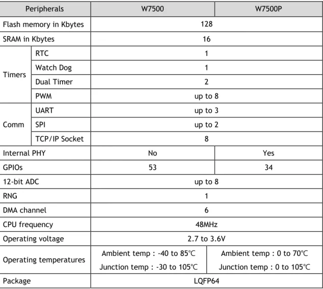
Table 1. W7500/W7500P family device features and peripheral counts
Peripherals W7500 W7500P
Flash memory in Kbytes 128
SRAM in Kbytes 16 Timers RTC 1 Watch Dog 1 Dual Timer 2 PWM up to 8 Comm UART up to 3 SPI up to 2 TCP/IP Socket 8
Internal PHY No Yes
GPIOs 53 34 12-bit ADC up to 8 RNG 1 DMA channel 6 CPU frequency 48MHz Operating voltage 2.7 to 3.6V
Operating temperatures Ambient temp : -40 to 85℃ Junction temp : -30 to 105℃
Ambient temp : 0 to 70℃
Junction temp : 0 to 105℃
3
Functional overview
3.1
ARM® -Cortex® -M0 core with embedded Flash and SRAM
The ARM® Cortex® -M0 processor is the latest generation of ARM processors for embedded systems. It has been developed to provide a low-cost platform that meets the needs of MCU implementation, with a reduced pin count and low-power consumption, while delivering outstanding computational performance and an advanced system response to interrupts. The ARM® Cortex® -M0 32-bit RISC processor features exceptional code-efficiency, delivering the high-performance expected from an ARM core in the memory size usually associated with 8- and 16-bit devices.
The W7500x family has an embedded ARM core and is therefore compatible with all ARM tools and software.
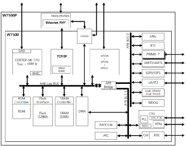
Figure 1 shows the general block diagram of the W7500x family.
3.2
Memories
Program memory, data memory, registers and I/O ports are organized within the same linear 4-Gbyte address space.
The bytes are coded in memory in Little Endian format. The lowest numbered byte in a word is considered the word’s least significant byte and the highest numbered byte the most significant.
3.3
Boot modes
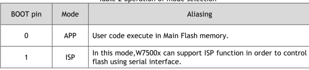
W7500x has three different boot modes that can be selected through the BOOT pin as shown in Table 2.
Table 2 operation of mode selection
BOOT pin Mode Aliasing
0 APP User code execute in Main Flash memory.
3.4
System configuration controller (SYSCFG)
Main purposes of the system configuration controller are the following The ability to enable an automatic reset if the system locks up
Information about the cause of the last reset
3.5
Power management
3.5.1
Power supply schemes
W7500x embeds a voltage regulator in order to supply the internal 1.5V digital power domain. Require a 2.7V ~ 5.5V operating supply voltage (VDD). ADC ref voltage is same as VDD
3.5.2
Low-power modes
W7500x is in RUN mode after a system or power reset. There are two low power modes to save power when the CPU does not need to be kept running. These modes are useful for instances like when the CPU is waiting for an external interrupt. Please note that there is no power-off mode for W7500x.
The device features two low-power modes:
Sleep mode
Deep Sleep mode
Additionally, the power consumption can be reducing by following method: User can slow down the system clocks
User can gate the clocks to the peripherals when they are unused. Sleep mode / Deep sleep mode
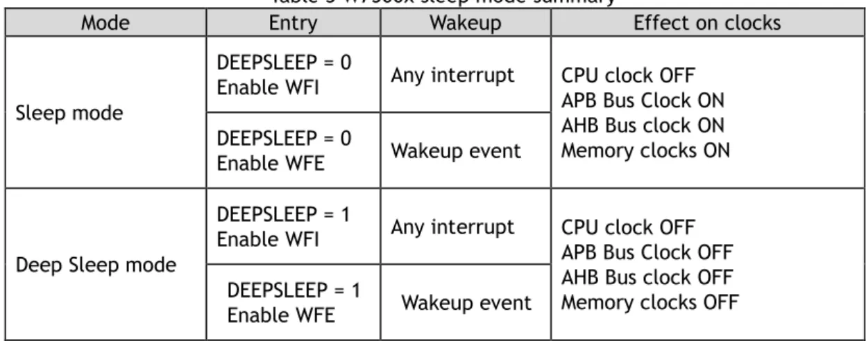
W7500x has two kinds of sleep modes. One is Sleep mode and the other is Deep sleep mode. Two of them are almost the same except the clock gated peripherals kinds. Table 3 shows the Sleep mode summary.
Table 3 W7500x sleep mode summary
Mode Entry Wakeup Effect on clocks
Sleep mode
DEEPSLEEP = 0
Enable WFI Any interrupt CPU clock OFF APB Bus Clock ON AHB Bus clock ON Memory clocks ON DEEPSLEEP = 0
Enable WFE Wakeup event
Deep Sleep mode
DEEPSLEEP = 1
Enable WFI Any interrupt CPU clock OFF APB Bus Clock OFF AHB Bus clock OFF Memory clocks OFF DEEPSLEEP = 1
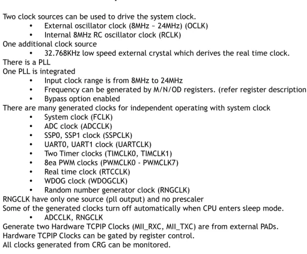
3.6
Clocks and startup
Two clock sources can be used to drive the system clock.
External oscillator clock (8MHz ~ 24MHz) (OCLK)
Internal 8MHz RC oscillator clock (RCLK) One additional clock source
32.768KHz low speed external crystal which derives the real time clock. There is a PLL
One PLL is integrated
Input clock range is from 8MHz to 24MHz
Frequency can be generated by M/N/OD registers. (refer register description)
Bypass option enabled
There are many generated clocks for independent operating with system clock
System clock (FCLK)
ADC clock (ADCCLK)
SSP0, SSP1 clock (SSPCLK)
UART0, UART1 clock (UARTCLK)
Two Timer clocks (TIMCLK0, TIMCLK1)
8ea PWM clocks (PWMCLK0 - PWMCLK7)
Real time clock (RTCCLK)
WDOG clock (WDOGCLK)
Random number generator clock (RNGCLK) RNGCLK have only one source (pll output) and no prescaler
Some of the generated clocks turn off automatically when CPU enters sleep mode.
ADCCLK, RNGCLK
Generate two Hardware TCPIP Clocks (MII_RXC, MII_TXC) are from external PADs. Hardware TCPIP Clocks can be gated by register control.
All clocks generated from CRG can be monitored.
3.6.1
External Oscillator Clock
The External oscillator clock (OCLK) can be supplied with a 8 to 24 MHz crystal/ceramic resonator oscillator. In the Typical application, Figure 3, 𝑅𝐹 must be inserted in External
oscillator clock circuit. In W7500x, there is no supported 𝑅𝐹 for External oscillator clock (see
Figure 3).
For 𝐶𝐿𝑜𝑎𝑑1 and 𝐶𝐿𝑜𝑎𝑑2, it is recommended to use external ceramic capacitors in the 5 pF to
25 pF range(typ.) and are usually the same size, designed for application, and selected to match the requirements of the crystal or resonator (see Figure 3).
Refer to the crystal resonator manufacturer for more details on the resonator characteristics (frequency, package, accuracy).
1 𝑅
𝐸𝑋𝑇 value depends on the crystal characteristics Figure 3 Typical application with an 8 MHz crystal
3.6.2
RC oscillator clock
RC oscillator clock (RCLK) signal is generated from an internal 8MHz RC oscillator.
RC oscillator has the advantage of providing a clock source at low cost (no external components). However the RC oscillator is less accurate than the external crystal or ceramic resonator.
Accuracy : 1% at TA= 25oC (User don’t need to calibration)
3.6.3
PLL
The internal PLL can be used to multiply the External Oscillator Clock (OCLK) or RC Oscillator Clock (RCLK). PLL input can be selected by register.
PLL output clock can be generated by following the equations below.
FOUT = FIN x M / N x 1 / OD Where: M = M[5] x 25 + M[4] x 24 + M[3] x 23 + M[2] x 22 + M[1] x 2 + M[0] x 1 N = N[5] x 25 + N[4] x 24 + N[3] x 23 + N[2] x 22 + N[1] x 2 + N[0] x 1 OD = 2 (2 x OD[1]) x 2 (1 x OD[0])
3.6.4
Generated clock
Each generated clock source can be selected among 3 clock source as independent by each clock source select register.
PLL output clock (MCLK)
Internal 8MHz RC oscillator clock (RCLK)
External oscillator clock (8MHz ~ 24MHz) (OCLK)
1 𝑅
Each generated clock has own prescaler which can be selected individually by each prescale value register.
FCLK, ADCCLK, SSPCLK, UARTCLK : 1/1, 1/2, 1/4, 1/8
TIMCLK0, TIMCLK1, PWMCLK0 – PWMCLK7, RTCCLK, WDOGCLK : 1/1, 1/2, 1/4, 1/8, 1/16, 1/32, 1/64, 1/128
3.7
Interrupts and events
3.7.1
Nested vectored interrupt controller (NVIC)
The W7500x family embeds a nested vectored interrupt controller able to handle up to 32 maskable interrupt channels (not including the 16 interrupt lines of Cortex® -M0) and 4 priority levels.
Closely coupled NVIC gives low latency interrupt processing
Interrupt entry vector table address passed directly to the core
Closely coupled NVIC core interface
Allows early processing of interrupts
Processing of late arriving higher priority interrupts
Support for tail-chaining
Processor state automatically saved
Interrupt entry restored on interrupt exit with no instruction overhead
This hardware block provides flexible interrupt management features with minimal interrupt latency.
3.7.2
Event controller
The W7500x family is able to handle internal events in order to wake up the core(WFE). The wakeup event can be generated by
When after DMA process finished (DMA_DONE)
3.8
Tcp/ip offload engine (TOE)
The TCP/IP Core Offload Engine (TOE) is a Hardwired TCP/IP embedded Ethernet controller that provides easier Internet connection to embedded systems. TOE enables users to have Internet connectivity in their applications by using the TCP/IP stack.
WIZnet’s Hardwired TCP/IP is the market-proven technology that supports TCP, UDP, IPv4, ICMP, ARP, IGMP, and PPPoE protocols. TOE embeds the 32Kbyte internal memory buffer for the Ethernet packet processing. Using TOE allows users to implement the Ethernet application by adding the simple socket program. It’s faster and easier than using any other Embedded Ethernet solutions. 8 independent hardware sockets can be used simultaneously.
TOE also provides WOL (Wake on LAN) to reduce power consumption of the system.
Supports Hardwired TCP/IP Protocols : TCP, UDP, ICMP, IPv4, ARP, IGMP, PPPoE
Supports 8 independent sockets simultaneously
Supports Power down mode
Supports Wake on LAN over UDP
Internal 32Kbytes Memory for TX/RX Buffers
3.9
General-purpose inputs/outputs (GPIOs)
The GPIO(General-Purpose I/O Port) is composed of three physical GPIO blocks, each corresponding to an individual GPIO port(PORT A, PORT B and PORT C). The GPIO supports up to 34 programmable input/output pins, depending on the peripherals being used.
The GPIO peripheral consists the following features.
GPIO_DATAOUT can SET/CLEAR by the SET register and CLEAR register. (1 for set and 0 for clear)
Mask registers allow treating sets of port bits as a group leaving other bits unchanged.
Up to 34 GPIOs depending on configuration
Programmable control for GPIO interrupts
Interrupt generation masking
Edge-triggered on rising, falling, or both
Refer to ‘Reference Manual’ for more details about each register.
3.10
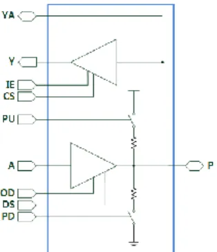
Pad controller (PADCON)
Pads of W7500x are controllable. User can control pad’s characteristic. W7500x has digital I/O pads and digital/analog mux I/O pads
Controllable characteristics of pads are pull-up, pull-down, driving strength, input enable, and CMOS/Schmitt trigger input buffer
Each pad can be controlled individually by register.
Figure 4 shows the function schematic of digital I/O pad of W7500x.
Figure 4. function schematic of digital I/O pad
Figure 5 shows the function schematic of digital/analog mux IO pad of W7500x
Initials of Pad diagram is same as below.
P - PAD
A – Digital Output
YA – Analog Input (connect to ADC input)
Y – Digital Input
IE – Input buffer enable
CS – CMOS/Schmitt trigger input buffer select
PU – Pull-up enable
PD – Pull-down enable
OD – Open Drain
DS – Driving strength select
User can set pad condition with IE, CS, PU/PD, OD, DS by register. And pads are can be controlled individually.
Condition A Y P
Input buffer enable (IE = 1)
Output mode OUT OUT OUT
Input mode No use IN IN
Input buffer disable (IE = 0)
Output mode OUT Low (0) OUT
Input mode No use IN IN
Condition Rise/Fall Time (nSec) Propagation Delay (nSec) Driving
Strength
Capacitan
ce loading Min Max Min Max
Low (DS = 1) 25pF 4 18 7 27 100pF 11 53 11 44 High (DS = 0) 25pF 1 8 4 16 100pF 4 23 7 24
3.11
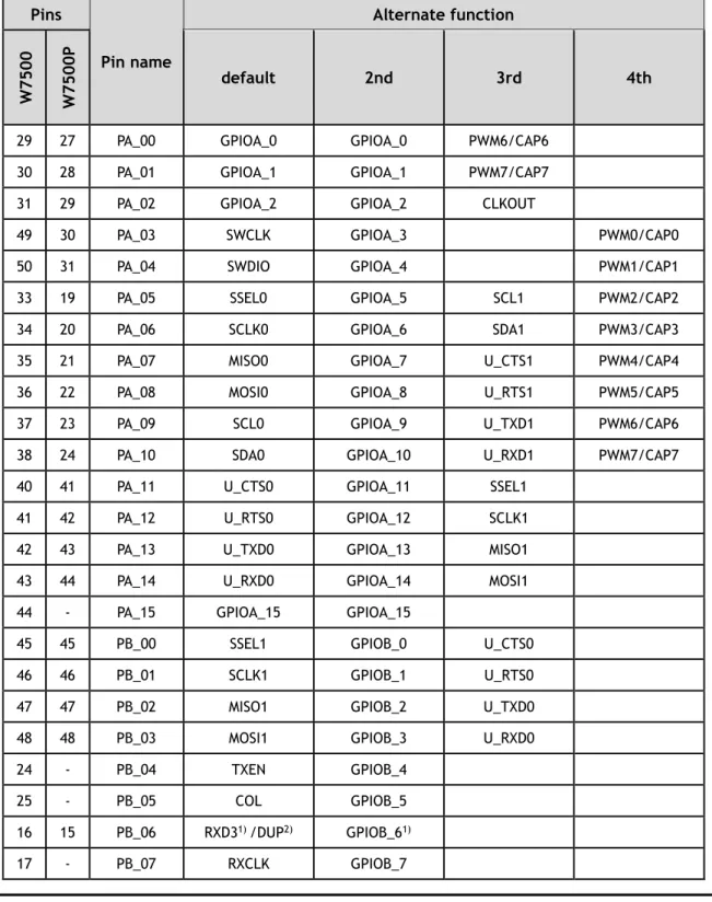
Alternative function controller (AFC)
Each functional PADs have several functions.Users can select a function in Alternate Function Controller block. Each functional pad has 2 ~ 4 functions.
Pads can be selected by each registers individually. Each pad can be used as an external interrupt source. Table 4 shows the function table of each functional pad.
Table 4 functional description table Pins Pin name Alternate function W 7 5 0 0 W 7 5 0 0 P default 2nd 3rd 4th
29 27 PA_00 GPIOA_0 GPIOA_0 PWM6/CAP6
30 28 PA_01 GPIOA_1 GPIOA_1 PWM7/CAP7
31 29 PA_02 GPIOA_2 GPIOA_2 CLKOUT
49 30 PA_03 SWCLK GPIOA_3 PWM0/CAP0
50 31 PA_04 SWDIO GPIOA_4 PWM1/CAP1
33 19 PA_05 SSEL0 GPIOA_5 SCL1 PWM2/CAP2
34 20 PA_06 SCLK0 GPIOA_6 SDA1 PWM3/CAP3
35 21 PA_07 MISO0 GPIOA_7 U_CTS1 PWM4/CAP4
36 22 PA_08 MOSI0 GPIOA_8 U_RTS1 PWM5/CAP5
37 23 PA_09 SCL0 GPIOA_9 U_TXD1 PWM6/CAP6
38 24 PA_10 SDA0 GPIOA_10 U_RXD1 PWM7/CAP7
40 41 PA_11 U_CTS0 GPIOA_11 SSEL1
41 42 PA_12 U_RTS0 GPIOA_12 SCLK1
42 43 PA_13 U_TXD0 GPIOA_13 MISO1
43 44 PA_14 U_RXD0 GPIOA_14 MOSI1
44 - PA_15 GPIOA_15 GPIOA_15
45 45 PB_00 SSEL1 GPIOB_0 U_CTS0
46 46 PB_01 SCLK1 GPIOB_1 U_RTS0
47 47 PB_02 MISO1 GPIOB_2 U_TXD0
48 48 PB_03 MOSI1 GPIOB_3 U_RXD0
24 - PB_04 TXEN GPIOB_4
25 - PB_05 COL GPIOB_5
16 15 PB_06 RXD31) /DUP2) GPIOB_61)
18 - PB_08 DUP GPIOB_8 19 - PB_09 TXCLK GPIOB_9 20 - PB_10 TXD0 GPIOB_10 21 - PB_11 TXD1 GPIOB_11 22 - PB_12 TXD2 GPIOB_12 23 - PB_13 TXD3 GPIOB_13 26 - PB_14 GPIOB_14 GPIOB_14 27 - PB_15 GPIOB_15 GPIOB_15
53 53 PC_00 U_CTS1 GPIOC_0 PWM0/CAP0
54 54 PC_01 U_RTS1 GPIOC_1 PWM1/CAP11)
55 55 PC_02 U_TXD1 GPIOC_2 PWM2/CAP2
56 56 PC_03 U_RXD1 GPIOC_3 PWM3/CAP31)
57 57 PC_04 SCL1 GPIOC_4 PWM4/CAP4
58 58 PC_05 SDA1 GPIOC_5 PWM5/CAP5
51 11 PC_06 GPIOC_6 GPIOC_6 U_TXD2
52 - PC_07 GPIOC_7 GPIOC_7 U_RXD2
1 1 PC_08 PWM0/CAP0 GPIOC_8 SCL0 AIN7
2 2 PC_09 PWM1/CAP1 GPIOC_9 SDA0 AIN6
3 3 PC_10 U_TXD2 GPIOC_10 PWM2/CAP2 AIN5
4 4 PC_11 U_RXD2 GPIOC_11 PWM3/CAP3 AIN4
5 5 PC_12 AIN3 GPIOC_12 SSEL0 AIN3
6 6 PC_13 AIN2 GPIOC_13 SCLK0 AIN2
7 7 PC_14 AIN1 GPIOC_14 MISO0 AIN1
8 8 PC_15 AIN0 GPIOC_15 MOSI0 AIN0
11 - PD_00 CRS GPIOD_0 12 - PD_01 RXDV GPIOD_1 13 - PD_02 RXD0 GPIOD_2 14 - PD_03 RXD1 GPIOD_3 15 - PD_04 RXD2 GPIOD_4 1) Only W7500 2) Only W7500P
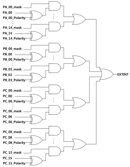
3.12
External interrupt (EXTI)
Each functional pads are connected to the external interrupt(EXTINT) source.
All functional pads can be used as an external interrupt source regardless of any set of pad function.
External Interrupt controller has the following functions and can be controlled by registers.
Interrupt mask (enable or disable, default : disable)
Interrupt polarity (rising or falling, default : rising)
All pads are connected to the control register individually. (External interrupt mask register and External Interrupt polarity register)
External interrupt working as following expression:
Each pad interrupt = Interrupt mask & (Interrupt polarity ^ Pad input)
EXTINT = any Each pad interrupt
Figure 6 shows the External Interrupt diagram.
PA_00_Polarity PA_00_mask PA_00 EXTINT . . . . . . PA_14_Polarity PA_14_mask PA_14 PB_00_Polarity PB_00_mask PB_00 . . . . . . PB_03_Polarity PB_03_mask PB_03 PC_00_Polarity PC_00_mask PC_00 . . . . . . PC_06_Polarity PC_06_mask PC_06 PC_08_Polarity PC_08_mask PC_08 . . . . . . PC_15_Polarity PC_15_mask PC_15
3.13
Direct memory access controller (DMA)
Direct memory access (DMA) is used in order to provide high-speed data transfer between peripherals and memory as well as memory to memory. Data can be quickly moved by DMA without any CPU actions. This keeps CPU resources free for other operations.
The DMA controller has up to 6 channels in total, each dedicated to managing memory access requests from one or more peripherals. It has an arbiter for handling the priority between DMA requests. For more details, refer to “PrimeCell® μDMA Controller (PL230)” from the Technical Reference Manual
• 6 channels
• Each channel is connected to dedicated hardware DMA requests and software trigger is also supported on each channel.
• Priorities between requests from the DMA channels are software programmable (2 levels consisting of high, default)
• Memory-to-memory transfer (software request only) • TCP/IP-to-memory transfer (software request only)
• SPI/UART-to-memory transfer (hardware request and software request) • Access to Flash, SRAM, APB and AHB peripherals as source and destination DMA request mapping
The hardware requests from the peripherals (UART0, UART1, SSP0, SSP1) are simply connected to the DMA. Refer to Table 5 which lists the DMA requests for each channel.
Table 5 Summary of the DMA requests for each channel
Channel 1 Channel 2 Channel 3 Channel 4 Channel 5 Channel 6 Hardware Request SSP0_TX SSP0_RX SSP1_TX SSP1_RX UART0_TX UART0_RX UART1_TX
UART1_RX NONE NONE
Software
Request(1) Support Support Support Support Support Support
Software request is the only way to use DMA for memory-to-memory or TCP/IP-to-memory.
3.14
Analog to digital converter (ADC)
ADC is a 12bit analog-to-digital converter. It has up to 9 multiplexed channels allowing it to measure signals from 8 externals and 1 internal source.
ADC of various channels can be performed in single mode. The result of the ADC is stored in 12 bit register.
12bit configuration resolution
Conversion time : Max 10MHz (Sampling time can be programmable)
8 channel for external analog inputs
1 channel for internal LDO(1.5v) voltage
Start of conversion can be initiated by software.
Convert selected inputs once per trigger.
3.15
Timers and watchdogs
3.15.1
System tick timer
System tick timer(SysTick) is part of the ARM Cortex-M0 core
Simple 24bit timer.
Clocked internally by the system clock or the system clock/2.
The SysTick timer is an integral part of Cortex-M0. The SysTick timer is intended to generated a fixed 10 millisecond interrupt for use by an operating system or other system management software.
Since the SysTick timer is a part of the Cortex-M0, it facilitates porting of software by providing a standard timer that is available on Cortex-M0 based devices.
The SysTick timer can be used for :
An RTOS tick timer which fires at a programmable rate (for example 100 Hz) and invokes a SysTick routine.
A high-speed alarm timer using the core clock.
A simple counter. Software can use this to measure time to completion and time used.
An internal clock source control based on missing/meeting durations. The COUNTFLAG bit-field in the control and status register can be used to determine if an action completed within a set duration, as part of a dynamic clock management control loop.
3.15.2
Pulse-Width Modulation (PWM)
The PWM consists a 8-channel 32-bit Timer/Counter driven by a programmable prescaler. The function of the PWM is based on the basic Timer. Each timer and counter runs independently. The PWM can be used to control the width of the pulse, formally the pulse duration, to generate output waveform or to count the counter triggered by external input.
Counter or Timer operation can use the peripheral clock, external clock source, or one of the capture inputs as the clock source.
Eight independent 32-bit Timer/Counter driven by a programmable 6 bits prescaler runs as the PWM or standard timer if the PWM mode is not enabled.
Eight PWM output waveforms.
Each of Timer/Counter can have different or same clock source.
Counter or timer operation.
Eight capture registers that can take the timer value when an external input signal. A capture event can generate an interrupt signal optionally.
32-bit match register and limit register.
3.15.3
Dual timers
The dual timer consists two programmable 32-bit or 16-bit Free-running counters(FRCs) that can generate interrupts when they reach 0. There are two dual timers and 4 FRCs. One dual timers has one interrupt handler, resulting in two interrupts of timers. Also one dual timer has one clock but two clock enable signals. Users can select one repetition modes one-shot or wrapping mode, and wrapping mode consists free-running and periodic mode. Two FRCs are one set so two FRCs has one clock, reset, and interrupt but each FRC has an individual clock enable.
One dual timer has two Free-Running Counters(FRCs).
One dual timer has two clock enable signals.
There are 2 dual timers.
A 32-bit or a 16-bit down counter.
One of the following repetition modes: one-shot and wrapping mode.
One of the following wrapping modes: Free-running and periodic mode.
There is a prescaler that can divide down the clock rate by 1, 16, or 256.
3.15.4
Watchdog timer
The watchdog is based on a 32-bit down-counter that is initialized from the Reload Register, WDTLoad. The watchdog generates a regular interrupt depending on a programmed value. The counter decreases by one on each positive clock edge of watchdog clock.
The watchdog monitors the interrupt and asserts a reset request signal when the counter reaches 0 and the counter is stopped. On the next enabled watchdog clock edge, the counter is reloaded from the WDTLoad Register and the countdown sequence continues. The watchdog reasserts the reset signal if the interrupt is not cleared by the time the counter next reaches 0.
The watchdog applies a reset to a system in the event of a software failure to provide a way to recover from software crashes. Users can enable or disable the watchdog unit as required.
32-bit down counter.
Internally resets chip if not periodically reloaded.
The watchdog timer has lock register to prevent rogue software from disabling the watchdog timer functionality.
The watchdog timer clock(WDTCLK) and system clock(PCLK) are synchronous.
3.16
Real-time clock (RTC)
The real-timer clock (RTC) is an independent BCD timer/counter. The RTC provides a timer-of-day clock/calendar with programmable alarm interrupt.
Calendar with year, month, day, weekday, hours, minutes, and seconds Programmable alarm with interrupt function
3.16.1
RTC clock
RTC Clock (RTCCLK) can be selected among several clocks (32768Hz oscillator, MCLK, RCLK, OCLK). Please refer to the Clock Reset Generator chapter for configuring the clock.
If the 32768Hz oscillator clock is used, the divider generates 1 Hz clock internally.
If the DIVRST (Bit[1] of RTC Control Register ) value is high, the RTC Divider is cleared. If the DIVRST value is low, the divider operates.
3.16.2
RTC interrupt
RTC has two kinds of interrupt source, Counter Interrupt and Alarm Interrupt.
Interrupts are enabled in the NVIC using the appropriate Interrupt Set Enable register. There are following Counter Interrupts: Second, Minute, Hour, Day (Day of Week), Date (Day of Month) and Year.
Each bit of RTCINTM (Interrupt Mask Register) can disable or enable interrupt for each Counter Interrupt.
3.17
Universal asynchronous receiver/transmitter (UART)
The device embeds three universal asynchronous receivers/transmitters (UART0, UART1, UART2) which communicate at speeds of up to 3 Mbit/s.
The UART supports synchronous one-way communication, half-duplex single wire communication, and UART0,1 supports multiprocessor communications(CTS/RTS) but UART2 unsupported multiprocessor communications UART2 is called the SUART(Simple UART).
Serial-to-parallel conversion on data received from a peripheral device
Parallel-to-serial conversion on data transmitted to the peripheral device
Data size of 5,6,7 and 8 its
One or two stop bits
Even, odd, stick, or no-parity bit generation and detection
Support of hardware flow control
Programmable FIFO disabling for 1-byte depth.
Programmable use of UART or IrDA SIR input/output
False start bit detection
UART bidirectional communication requires a minimum of two pins: RX, TX The frame are comprised of:
An Idle Line prior to transmission or reception
A start bit
A data word (8 or 9 bits) least significant bit first
1, 1.5, 2 Stop bits indicating that the frame is complete
The USART interface uses a baud rate generator
A status register (UART1_RISR)
data registers (UART1DR)
A baud rate register (UART1_IBRD,UART1_FBRD)
3.18
Synchronous Serial Port (SSP)
The SSP block is an IP provided by ARM (PL022 “PrimeCell® Synchronous Serial Port”).
Additional details about its functional blocks may be found in “ARM PrimeCell® Synchronous Serial Port (PL022) Technical Reference Manual”.
The SSP is a master or slave interface that enables synchronous serial communication with slave or master peripherals having one of the following:
A MOTOROLA SPI-compatible interface
A TEXAS INSTRUMENTS synchronous serial interface
A National Semiconductor MICROWIRE® interface.
The SPI interface operates as a master or slave interface. It supports bit rates up to 20 MHz in master mode and up to 4 MHz in slave mode.
Parallel-to-serial conversion on data written to an internal 16-bit wide, 8- location deep transmit FIFO
Serial-to-parallel conversion on received data, buffering it in a 16-bit wide, 8-location deep receive FIFO
Programmable data frame size from 4 to 16 bits
Programmable clock bit rate and prescaler. The input clock may be divided by a factor of 2 to 254 in steps of two to provide the serial output clock
3.19
Random number generator (RNG)
RNG is a 32bit random number generator. RNG generates power on random number when power on reset. RNG can run/stop by software. RNG seed value and polynomial of RNG can be modified by software.
32bit pseudo random number generator
Formula of pseudo random number generator (polynomial) can be modified.
Seed value of random generator can be modified.
Support power on reset random value.
4
Pinout and descriptions
4.1
Pin layout
Figure 7 W7500 pin layout
4.2
Pin descriptions
4.2.1
W7500 Pin Description
Table 6. Pin Type Notation
Type Description I Input O Output IO Input/Output A Analog PWR Power GND Ground
Table 7 W7500 Pin Description
PIN No Symbol Type
Function Main Function 2nd Function 3rd Function 4th Function
1 PC_08 AIO PWM0/CAP0 GPIO3_8 SCL0 AIN7
2 PC_09 AIO PWM1/CAP1 GPIO3_9 SDA0 AIN6
3 PC_10 AIO U_TXD2 GPIO3_10 PWM2/CAP2 AIN5
4 PC_11 AIO U_RXD2 GPIO3_11 PWM3/CAP3 AIN4
5 PC_12 AIO AIN3 GPIO3_12 SSEL0 AIN3
6 PC_13 AIO AIN2 GPIO3_13 SCLK0 AIN2
7 PC_14 AIO AIN1 GPIO3_14 MISO0 AIN1
8 PC_15 AIO AIN0 GPIO3_15 MOSI0 AIN0
9 GND GND GND 10 VDD PWR VDD 11 PD_00 IO CRS/TXD3 GPIO4_0 12 PD_01 IO RXDV/TXD2 GPIO4_1 13 PD_02 IO RXD0/TXD1 GPIO4_2 14 PD_03 IO RXD1/TXD0 GPIO4_3 15 PD_04 IO RXD2/TXCLK GPIO4_4 16 PB_06 IO RXD3/DUP GPIO2_6 17 PB_07 IO RXCLK/RXCLK GPIO2_7 18 PB_08 IO DUP/RXD3 GPIO2_8 19 PB_09 IO TXCLK/RXD2 GPIO2_9
PIN No Symbol Type Function Main Function 2nd Function 3rd Function 4th Function 20 PB_10 IO TXD0/RXD1 GPIO2_10 21 PB_11 IO TXD1/RXD0 GPIO2_11 22 PB_12 IO TXD2/RXDV GPIO2_12 23 PB_13 IO TXD3/CRS GPIO2_13 24 PB_04 IO TXEN GPIO2_04 25 PB_05 IO COL GPIO2_05 26 PB_14 IO MDIO/MDC GPIO2_14 27 PB_15 IO MDC/MDIO GPIO2_15 28 RSTn I RSTn
29 PA_00 IO GPIO1_0 GPIO1_0 PWM6/CAP6
30 PA_01 IO GPIO1_1 GPIO1_1 PWM7/CAP7
31 PA_02 IO GPIO1_2 GPIO1_2 CLKOUT
32 TEST IO TEST
33 PA_05 IO SSEL0 GPIO1_5 SCL1 PWM2/CAP2
34 PA_06 IO SCLK0 GPIO1_6 SDA1 PWM3/CAP3
35 PA_07 IO MISO0 GPIO1_7 U_CTS1 PWM4/CAP4
36 PA_08 IO MOSI0 GPIO1_8 U_RTS1 PWM5/CAP5
37 PA_09 IO SCL0 GPIO1_9 U_TXD1 PWM6/CAP6
38 PA_10 IO SDA0 GPIO1_10 U_RXD1 PWM7/CAP7
39 BOOT IO BOOT
40 PA_11 IO U_CTS0 GPIO1_11 SSEL1
41 PA_12 IO U_RTS0 GPIO1_12 SCLK1
42 PA_13 IO U_TXD0 GPIO1_13 MISO11
43 PA_14 IO U_RXD0 GPIO1_14 MOSI1
44 PA_15 IO GPIO1_15 GPIO1_15
45 PB_00 IO SSEL1 GPIO2_0 U_CTS0
46 PB_01 IO SCLK1 GPIO2_1 U_RTS0
PIN No Symbol Type Function Main Function 2nd Function 3rd Function 4th Function
48 PB_03 IO MOSI1 GPIO2_3 U_RXD0
49 PA_03 IO SWCLK GPIO1_3 PWM0/CAP0
50 PA_04 IO SWDIO GPIO1_4 PWM1/CAP1
51 PC_06 IO GPIO3_6 GPIO3_6 U_TXD2
52 PC_07 IO GPIO3_7 GPIO3_7 U_RXD2
53 PC_00 IO U_CTS1 GPIO3_0 PWM0/CAP0
54 PC_01 IO U_RTS1 GPIO3_1 PWM1/CAP1
55 PC_02 IO U_TXD1 GPIO3_2 PWM2/CAP2
56 PC_03 IO U_RXD1 GPIO3_3 PWM3/CAP3
57 PC_04 IO SCL1 GPIO3_4 PWM4/CAP4
58 PC_05 IO SDA1 GPIO3_5 PWM5/CAP5
59 GND GND GND
60 NC NC NC
61 VDD PWR VDD
62 GND GND GND
63 XTAL_IN I Xtal in
4.2.2
W7500P Pin Description
Table 8. W7500P Pin Description
PIN No Symbol Type
Function Main Function 2nd Function 3rd Function 4th Function PHY
1 PC_08 AIO PWM0/CAP0 GPIO3_8 SCL0 AIN7
2 PC_09 AIO PWM1/CAP1 GPIO3_9 SDA0 AIN6
3 PC_10 AIO U_TXD2 GPIO3_10 PWM2/CAP2 AIN5
4 PC_11 AIO U_RXD2 GPIO3_11 PWM3/CAP3 AIN4
5 PC_12 AIO AIN3 GPIO3_12 SSEL0 AIN3
6 PC_13 AIO AIN2 GPIO3_13 SCLK0 AIN2
7 PC_14 AIO AIN1 GPIO3_14 MISO0 AIN1
8 PC_15 AIO AIN0 GPIO3_15 MOSI0 AIN0
9 VSS GND VSS
10 VDD PWR VDD
11 PC_06 IO GPIO3_6 GPIO3_6 U_TXD2
12 TEST IO TEST
13 REGIN PWR REGIN
14 LED_0 IO LED_0 LED_0
15 PB_06/DUP IO DUP DUP
16 VSS IO VSS
17 LED_3 IO LED_3 LED_3
18 VDD PWR VDD_IO
19 PA_05 IO SSEL0 GPIO1_5 SCL1 PWM2/CAP2
20 PA_06 IO SCLK0 GPIO1_6 SDA1
21 PA_07 IO MISO0 GPIO1_7 U_CTS1 PWM4/CAP4
22 PA_08 IO MOSI0 GPIO1_8 U_RTS1 PWM5/CAP5
23 PA_09 IO SCL0 GPIO1_9 U_TXD1 PWM6/CAP6
24 PA_10 IO SDA0 GPIO1_10 U_RXD1 PWM7/CAP7
25 VSS IO VSS_IO
PIN No Symbol Type Function Main Function 2nd Function 3rd Function 4th Function PHY
27 PA_00 IO GPIO1_0 GPIO1_0 PWM6/CAP6
28 PA_01 IO GPIO1_1 GPIO1_1 PWM7/CAP7
29 PA_02 IO GPIO1_2 GPIO1_2 CLKOUT
30 PA_03 IO GPIO1_3 GPIO1_3 PWM0/CAP0
31 PA_04 IO GPIO1_4 GPIO1_4
32 ISET I ISET ISET
33 AGND GND AGND
34 MDI_RN IO MDI_RN MDI_RN
35 MDI_RP IO MDI_RP MDI_RP
36 REGOUT PWR REGOUT
37 MDI_TN IO MDI_TN MDI_TN
38 MDI_TP IO MDI_TP MDI_TP
39 AGND GND AGND
40 AVDD PWR AVDD
41 PA_11 IO U_CTS0 GPIO1_11 SSEL1
42 PA_12 IO U_RTS0 GPIO1_12 SCLK1
43 PA_13 IO U_TXD0 GPIO1_13 MISO1
44 PA_14 IO U_RXD0 GPIO1_14 MOSI1
45 PB_00 IO SSEL1 GPIO2_0 U_CTS0
46 PB_01 IO SCLK1 GPIO2_1 U_RTS0
47 PB_02 IO MISO1 GPIO2_2 U_TXD0
48 PB_03 IO MOSI1 GPIO2_3 U_RXD0
49 VSS PWR VSS_IO 50 XPHY_IN I 25MHz xtal in 51 XPHY_OUT O 25MHz xtal out 52 BOOT IO BOOT
53 PC_00 IO U_CTS1 GPIO3_0 PWM0/CAP0
PIN No Symbol Type Function Main Function 2nd Function 3rd Function 4th Function PHY
55 PC_02 IO U_TXD1 GPIO3_2 PWM2/CAP2
56 PC_03 IO U_RXD1 GPIO3_3
57 PC_04 IO SCL1 GPIO3_4 PWM4/CAP4
58 PC_05 IO SDA1 GPIO3_5 PWM5/CAP5
59 XTAL32_IN I 32768Hz xtal in 60 XTAL32_OUT O 32768Hz xtal out 61 VDD PWR VDD 62 VSS GND VSS 63 XTAL_IN I Xtal in
5
Electrical characteristics
5.1
Absolute maximum ratings
These are stress ratings only and functional operation of the device at these conditions is not implied. Exposure to maximum rating conditions for extended periods may affect device reliability.
5.2
Voltage Characteristics
Table 9 shows the voltage characteristics of W7500x.
Table 9 Voltage characteristics
Symbol Ratings Min Max Unit
VDD-VSS Main supply voltage (VDD) -0.3 3.6 V
VIN Input voltage on IO pins VSS – 0.3 3.6 V
SVDDH I/O Power on slope 5V/Sec 1V/uSec -
∆VDD Variations between difference VDD power pins 50 mV
∆VSS Variations between different ground pins 50 mV
5.3
Current Characteristics
Table 10 shows the current characteristics of W7500x.
Table 10 Current characteristics
Symbol Ratings Max Unit
IVDD_SUM Total current into sum of all VDD power lines (source) 100 mA
IVDD Maximum current into each ADD power pin (source) 90 mA
IIO_PAD Total output current sunk by sum of all IOs and control pins 75 mA
IINJ_PAD Single pin input injected current ±10 mA
5.4
Thermal Characteristics
Table 11 shows the thermal characteristics of W7500x.
Table 11 Thermal Charateristics
Symbol Ratings Min Max Unit
TStorge Storage temperature range -55 150
℃ TJunc
Maximum junction temperature under bias
W7500 -40 150 W7500P 0 125 TA Ambient Operating Temperature W7500 -40 85 W7500P 0 70
5.5
Operating conditions
5.5.1
General Operating Conditions
Table 12 shows the general operating conditions of W7500x. Table 12 General operating conditions
Symbol Parameter Conditions Min Max Unit
fFCLK Internal CPU clock frequency 0 48 MHz
VDD Standard operating voltage 2.7 3.6 V
5.6
Supply Current Characteristics
Normal operationTable 13 shows the Normal operation supply current.
Table 13 Normal operation supply current
Symbol Parameter Conditions1 Condition2 Typ Unit
IDD_NOR current Supply
Active mode; code While(1) {} Executed from flash
memory System clock = 10MHz 6.14 (52.14) (1) (22.14) (2) mA System clock = 20MHz 8.82 (54.82) (1) (24.82) (2) mA System clock = 40MHz 14.09 (60.09) (1) (30.09) (2) mA
(1) When PHY Normal mode, W7500P Internal PHY power consumption is 46mA MAX.
(2) When PHY Power down mode, W7500P Internal PHY power consumption is 16mA MAX.
Sleep mode
Table 14 shows the Normal operation supply current.
Table 14 Sleep mode supply current
Symbol Parameter Conditions1 Condition2 Typ Unit
IDD_SLP current Supply
After enter sleep mode All peripheral clocks ON (same as system clock)
System clock = 10MHz 3.51 (49.51) (1) (19.51) (2) mA System clock = 20MHz 5.65 (51.65) (1) (21.65) (2) mA System clock = 40MHz 9.61 (55.61) (1) (25.61) (2) mA
(3) When PHY Normal mode, W7500P Internal PHY power consumption is 46mA MAX.
(4) When PHY Power down mode, W7500P Internal PHY power consumption is 16mA MAX.
Deep sleep mode
Table 15 shows the deep sleep mode operation supply current. Table 15 Deep sleep mode supply current
Symbol Parameter Conditions1 Condition2 Typ Unit
IDD_DSLP current Supply After enter deep sleep mode All peripheral clocks OFF -
2.49 (48.49) (1)
(18.49) (2)
mA
(5) When PHY Normal mode, W7500P Internal PHY power consumption is 46mA MAX.
5.7
I/O PAD Characteristics
DC SpecificationTable 16 shows the DC specification of W7500x I/O PAD. Table 16 DC specification of PAD
Symbol Parameter Conditions Min Max Unit
VIH I/O Input high voltage 2.145 V
VIL I/O Input low voltage 1.155 V
VHYS Schmitt trigger hysteresis 0.33 V
IIH I/O Input high current 1 uA
IIL I/O Input low current -1 uA
VOH I/O Output high voltage
High driving strength Iload = 6mA
Low driving strength Iload = 3mA
2.5 V
VOL I/O Output low voltage
High driving strength Iload = 6mA
Low driving strength Iload = 3mA
0.5 V
Rpup
Rpdn
Pull-up
/Pull-down resistor 20 100 KOhm
Flash memory
Table 17 shows the flash memory reliability characteristics of W7500x Table 17 Flash memory Reliability Characteristics
Symbol Parameter Min Unit
NEND Sector Endurance 10,000 Cycles
TDR Data Retention 10 Years
5.8
Electrical Sensitivity Characteristics
Electostatic discharge (ESD)
Table 18 shows the ESD information of W7500x
Table 18 Electrostatic discharge (ESD)
Symbol Parameter Test Method Min Max Unit
VESD(HBM) Electostatic discharge (Human body model) AEC-Q100-002 ±2000 - V
VESD(CDM) Electostatic discharge (Charge device model) AEC-Q100-011 ±500 - V
Static latch-up
Table 19 shows the Static latch-up information of W7500x Table 19 Static latch-up
Symbol Parameter Test Method Min Max Unit
ILAT Latch up current at 125℃ ambient
temperature
5.9
Reset & PLL Characteristics
PLL Electrical characteristicsTable 20 shows the PLL characteristics of W7500x
Table 20 PLL electrical characteristics
Symbol Parameter Min Max Unit
td RSTn to PD delay time 5 - us
trst Reset pulse width 2 - us
tlock Lock time - 0.2 ms
Notice:
PLL_PDR[0] is LSB of PLL_PDR. please refer from Reference Manual. lock signal is internal signal.
1, td is the RSTn to PLL_PDR[0] delay time, which need larger than 5us.
2, trst is the reset pulse width, which need larger than 2us.
3, tlock is the lock time, which is less than 0.2ms.
4, When PLL_PDR[0] changes from “1” to “0”, the lock signal stays in “1” until a reset pulse comes. But the PLL is in unlocked state during this period.
5.10
ADC Characteristics
ADC Electrical characteristicsTable 21 shows the ADC electrical characteristics of W7500x Table 21 ADC electrical characteristics
Symbol Parameter Conditions Min Typ Max Unit
IN[15:0] Analog input channel VSS - VREFP V
VREFP Reference voltage of REFP VDD V
RES Resolution 12 Bits
Offset error -3.0 ±1.5 3.0 LSB
INL Integral non-linearity error -2.0 ±1.0 2.0 LSB
DNL Differential non-linearity error -1.0 ±0.8 1.5 LSB
Fclk Clock frequency 16 MHz
SPS Sampling rate 30 500 1000 K
TS Sampling time 4/Fclk
TC Conversion time 12 1/Fclk
SNDR Signal-noise plus distortion ratio At 10KHz 64 dB
THD Total harmonic distortion At 10Khz -65 dB
SFDR Spurious-free dynamic range At 10KHz 64 dB
ADC Transform function description
4095LSB 4093. 5LSB ADC input 4094. 5LSB 0.5LSB 2.5LSB 1.5LSB 000 000 000 000 000 000 000 001 000 000 000 010 111 111 111 101 111 111 111 110 111 111 111 111 ADC output
5.11
SSP Interface Characteristics
The maximum SSP speed is 20 Mbit/s in master mode or 4 Mbit/s in slave mode. In slave mode, the maximum SSP clock rate must be 1/12 of the SSP PCLK clock rate.
Table 22 shows the SSP characteristics of W7500x.
Table 22 SSP characteristics
Symbol Parameter Min Nom Max Unit
tclk_per SSPCLK cycle time 2 65024 System clocks
tclk_high SSPCLK high time - 0.5 t clk_per
tclk_low SSPCLK low time - 0.5 t clk_per
tclkrf SSPCLK rise/fall time - 6 10
tDMd Data from master valid delay time 0 - 1 System clocks
tDMs Data from master setup time 1 - - System clocks
tDMh Data from master hold time 2 - - System clocks
tDSs Data from slave setup time 1 - - System clocks
tDSh Data from slave hold time 2 - - System clocks
6
Package Information
6.1
Package dimension information
Figure 12 shows the package dimension information.
Document History Information
Version Date Descriptions
Ver. 1.0.0 18SEP2017 Initial Release
Ver. 1.0.1 26OCT2017 Fixed value Driving Strength condition in PADCON.
Ver. 1.0.2 09NOV2017 Fixed Typo I/O Pad Characteristics VOL description (high -> low)
Ver. 1.0.3 30NOV2017 Fixed figure 8. (W7500P Pin out)
Ver. 1.0.4 18DEC2017 Add Reset & PLL characteristics.
Ver. 1.0.5
30JAN2018
1. Fixed figure 8 (W7500P Pin layout) / Added subhead (4.2.1 W7500, 4.2.2 W7500P) / Fixed table 8(modified Symbol name) 2. Modified SRAM description (2. Description)
Ver. 1.0.6 05FEB2018 Add info about W7500P power consumption.(Current Characteristics)
Copyright Notice
Copyright 2017 WIZnet Co., Ltd. All Rights Reserved. Technical Support: https://forum.wizwiki.io/
Sales & Distribution: [email protected]