Volume 2010, Article ID 817201,5pages doi:10.1155/2010/817201
Research Article
Study of Radiative Defects Using Current-Voltage Characteristics
in ZnO Rods Catalytically Grown on 4H-p-SiC
N. Bano,
1I. Hussain,
1O. Nur,
1M. Willander,
1and P. Klason
21Department of Science and Technology, Norrk¨oping Campus, Link¨oping University, 60174 Norrk¨oping, Sweden
2Department of Physics, Gothenburg University, 412 96 Gothenburg, Sweden
Correspondence should be addressed to N. Bano,[email protected]
Received 22 February 2010; Revised 10 May 2010; Accepted 21 June 2010 Academic Editor: Ali Eftekhari
Copyright © 2010 N. Bano et al. This is an open access article distributed under the Creative Commons Attribution License, which permits unrestricted use, distribution, and reproduction in any medium, provided the original work is properly cited.
High-quality ZnO rods were grown by the vapour-liquid-solid (VLS) technique on 4H-p-SiC substrate. The current transport mechanisms of the diodes at room temperature (RT) have been explained in term of the space-charge-limited current model based on the energy band diagram of ZnO rods/4H-p-SiC heterostructure. The tunneling mechanism via deep-level states was found to
be the main conduction process at low-applied voltage but at trap-filled limit voltage VTFLall traps are filled and the
space-charge-limited current conduction dominated the current transport. From the RT current voltage measurements, the energy of the deep
level trap and the trap concentration were obtained as∼0.24±0.02 eV and 4.4×1018cm-3, respectively. The deep level states
observed correspond to zinc interstitial (Zni), responsible for the violet emission.
1. Introduction
Zinc oxide (ZnO) with wurtzite structure has a large direct bandgap around 3.4 eV, and a large exciton binding energy (60 meV), has recently attracted global interest, especially in its nanostructure form [1]. This material is famous for its photonic and electronic applications such as UV light emitters/detectors and as high-power and high-temperature devices [2, 3]. ZnO has a number of other advantages compared to other wide band gap semiconductors includ-ing high-thermal/chemical stabilities; the possibility of wet chemical etching and existence of large area wafers have all led to the demonstration of ZnO as an alternative material to nitride semiconductors [2,4]. Moreover, ZnO in its nanostructure form possesses self-organization growth property which facilitates the growth of ZnO nanostructures on any substrates such as glass, plastic, Si, GaN, AlGaN, and SiC. Among these materials 4H-SiC is a good candidate for the growth of n-ZnO rods because it has a similar energy bandgap.
ZnO possesses a rich family of nanostructures such as nanorods (NRs), nanoparticles, nanotips, and nanoneedles, as some examples [2,5–7]. All such nanostructures have been successfully synthesized and have attracted interest because
they can be used as building blocks for different future optoelectronic devices. These nanostructures have many advantages among which are large surface area to volume ratio, good crystal quality and unique photonic properties [8,9]. So far, among these structures, rods of ZnO is grown with relatively better crystalline quality with lower defect density compared to bulk and thin films due to their small foot print and the release of strain and stress due to the large surface area to volume ratio. At the same time, both ends of ZnO rods are extremely smooth, making them perfect mirror planes and vertical rods are like natural waveguide cavities for making the emitted light to travel to the top of the device, also minimizing partial leakage and thus enhancing the light extraction efficiency from the surface [10]. The dominant radiative defects in ZnO are oxygen vacancies (VO), zinc vacancies (VZn), zinc interstitials (Zni),
oxygen interstitials (Oi), zinc antisites (ZnO), and other
extrinsic impurities [11]. The free carrier concentration and luminescence efficiency are directly or indirectly related to these defects [11]. ZnO rods-based optical/electrical devices depend upon the defect chemistry and the understanding of the electrical properties, both of which are the subject of present theoretical and experimental studies. It is therefore essential to study the electrical transport properties of ZnO
Al ZnO rods PMMA layer Ni/Al p-SiC n-SiC
Figure 1: Schematic illustration of ZnO/p-SiC rods heterostructure device.
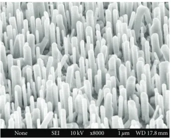
None SEI 10 kV x8000 1μm WD 17.8 mm
Figure 2: SEM image of ZnO rods grown on 4H-SiC substrate.
rods to establish ZnO rods-based devices. The electrical transport mechanism in ZnO rods grown on SiC has not yet been extensively studied nor thoroughly understood. However, to our best knowledge, only few authors reported electrical characteristic of ZnO thin films and rods on Si, SiC, and polymer substrates [12–15].
In this study, we report the investigation of the current transport mechanism of ZnO rods /p-SiC heterojunction diode at room temperature (RT) in terms of the space-charge-limited current model based on the energy band diagram of the heterostructure. From the RT current voltage measurements, the energy of the dominating deep level trap and its trap concentration were also calculated.
2. Experimental
ZnO rods were grown on a type SiC thin film. The p-type SiC film was grown by conventional chemical vapour deposition (CVD) technique on n-SiC commercial substrate [16]. The acceptor concentration in the p-SiC thin film was around 5×1018cm−3 and the thickness was around
1μm. The ZnO rods were grown by the vapour-liquid-solid (VLS) technique. First we cover a small portion of the p-SiC substrate for defining ohmic contacts on the p-SiC. After that a layer of 5 nm thick Au film was deposited on the p-type SiC. Then ZnO (99.99%) powder was mixed with graphite (99.99%) powder with 1 : 1 ratio with respect to the weight. This mixed powder was then vaporized. The substrate coated with Au was placed above the mixture, with the catalyst pointing towards to ZnO and graphite mixed powder. The growth was carried out in a horizontal tube furnace and the boat was placed in the middle of the quartz tube. To maintain a stable environment inside the tube, a constant Ar gas flow of 80 sccm was applied for 5–10 minutes. Then the growth was initiated at 890◦C and continued for 30 minutes. After growth the samples were processed for devices. For the ohmic contact on substrate first we cleaned the small portion of the p-SiC which was covered before the growth of the ZnO rods after that a thin layer of Ni\Al was used. The contact was annealed at 900◦C for 3 minutes in Ar atmosphere. Prior to the ohmic contacts on the ZnO rods an insulating PMMA layer was deposited between the rods. To ensure that no PMMA was on the top of the rods oxygen plasma cleaning was performed prior to the contact metal deposition. Then Al contacts of a diameter 0.5 mm were evaporated onto a group of rods. The configuration of the device is illustrated schematically in Figure 1. The device structure was characterized by scanning electron microscope (SEM) and at room temperature (RT) using two-point probe current-voltage (I–V) characteristics.
3. Results and Discussion
The ZnO rods were grown vertically aligned as shown in the SEM image inFigure 2. The diameter of the grown ZnO rods was found to be 200 nm and up to close to 600 nm, while the length was found to be around 1.9μm.Figure 3shows an equilibrium energy band diagram of p-n heterojunction of p-4H-SiC and n-ZnO. Here the bandgap (Eg) of ZnO is 3.3 eV and that of 4H-SiC is 3.23 eV. The conduction band offset (ΔEC) for electrons isΔEC =χZnO−χSiC=0.3 eV,
whereχis the electron affinity. While the valance band offset (ΔEV) for holes isΔEV=Eg (ZnO) +ΔEC−Eg (SiC)=0.4 eV.
ΔEVhas a higher value thanΔEC, which means that electron
injection from n-ZnO to p-SiC is larger than hole injection from p-SiC to n-ZnO [12].
Figure 4show that the resulting heterojunction exhibited good rectifyingI-Vcharacteristics. Such type of rectification behavior is best described by the thermionic emission theory. According to this theory, the current in such device could be expressed as I=Is exp q(V−IRs) nkT −1 , (1)
whereIsis the saturation current,Rsis the series resistance,
kis the Boltzmann constant,Tis the absolute temperature,
qis the elementary electric charge,V is the applied voltage, andnis the ideality factor.
Vacuum level χn-ZnO=4.35 eV Egn-ZnO=3.3 eV n-ZnO χp-4H-SiC=4.05 eV Egp-4H-SiC=3.23 eV ΔEc Ec Ef Ev ΔEv 4H-p-SiC
Figure 3: It shows a typical fabricated band diagram of p-n hetero junction of 4H-p-SiC and n-ZnO.
6 4 2 0 −2 −4 −6 Voltage (V) 0 2 4 ×10⁻⁶ Cu rr en t (A ) 6 4 2 0 Voltage (V) 0 2 4 6× 10⁵ dV/dI (Ohm)
Figure 4: Typical current-voltage characteristics for ZnO rods and the inset is the diode resistance dV/dI as a function of voltage.
The diode series resistance defined as Rs = dV/dI is
shown in Figure 4 (Inset). Below the turn-on voltage, Rs
decreases with increasing the forward bias. Then it maintains a constant value above the turn-on voltage. Under the forward bias the conduction band barrier will be decreased and will enhance the electron flow from the n-ZnO to the p-SiC and holes from the p-SiC to the n-ZnO. The successive recombination would give rise to the forward bias current flow. This means that the diode resistance would firstly decrease upon the increase of the forward bias voltage (i.e., the lowering of the barrier). As the forward bias is large enough, the barrier is negligible; the diode resistance becomes constant, which is due to the bulk material series resistance [17]. The slow rise in the forward current under low bias could be explained by the division of the voltage of the nonideal contact between the Al electrode and ZnO rods.
101 100 10−1 10−2 Voltage (V) 10−10 10−9 10−8 10−7 10−6 10−5 Cu rr en t (A ) 1 2 3 I∼V Von I∼exp (cV) VTFL I∼V2.5
Figure 5: Log-log plot for the I-V data of ZnO rods.
Using different diodes (5 diodes) the ideality factor obtained from (1) was found to be in the range 3-4. The higher value of the ideality factor indicates that the transport mechanism is no longer dominated by the thermionic emission. Nonideal behavior is often attributed to defect states in the band gap of the semiconductor providing other current transport mechanisms such as structural defects, surface contamination, barrier tunneling, or generation recombination in the space charge region and to variations in the interface composition [18,19]. To understand which mechanisms influence the junction behavior, theI-V char-acteristics of the device are studied in a log-log scale.
The log-log plot of the I-V data at RT is shown in Figure 5 and it illustrates that the current transport mechanism is exhibited in three different regions. The current in region 1 follows a linear dependence, that is, I∼V. This is an indication that the current transport is dominated by tunneling at low voltages. The boundary for this region was determined to be below 0.06 V. In region 2 (0.06-1 V) the current increases exponentially as I∼exp (cV). The ideality factor (3-4) is determined in this region and the dominating transport mechanism is recombination tunneling. Finally above 1 V (region 3) the current follows a power law (I∼V2.5), indicating a space-charge-limited
current transport mechanism. Space-charge-limited current (SCLC) and at least one of the other regions observed in the present study have been reported in different n-ZnO rods/p-Si heterojunction [13,17,20] and in Schottky contact to ZnO rods [14].
Lampert and Mark [21] have developed the single carrier (SCLC) model with the presence of a trap above the Fermi level. As the applied voltage V is lower than the onset voltage Von (V < Von) the thermally generated carrier density no
dominates over the injected carrier density and the carrier transit timeτx=d2/μVon(whereμis the electron mobility and
d is the depletion width) is larger than the dielectric or ohmic relaxation time τΩ= εεo/qnoμ, where εo,ε is permeability
thus undergo dielectric relaxation to maintain the charge neutrality rather than transport across the sample. In this region, the trap levels are not completely filled. For V >
Von the carriers transit time is smaller than the dielectric
relaxation time (τx< τΩ) and the injected carriers dominate
over the thermally generated carriers. The increase of the applied voltage also shifts the quasi-Fermi level towards the conduction band and the effect would be the filling up of the trap at an energy level Ec−Et, [17,21]. At an applied
voltage of V> VTFL(TFL stands for trap filled limit) all the
trap levels are filled and the conduction would become space charge limited and the current follows the Mott and Gurney SCLC expression [22] J= 9εεoμAV2 8d3 , (2)
where J is current density, μ is field-independent carrier mobility; d is the thickness of active layer,Ais the area,εis the dielectric, constant andεois the permittivity of free space.
The trap filled limit voltageVTFLis given as [21]
VTFL =nt qd
2
2εεo
, (3)
where Nt is the concentration of the unoccupied states
(trap concentration), located approximately at the estimated effective Fermi level. The effective carrier concentrationnoin
the active region is given by the expression
J(2VTFL)
J(VTFL) ∼
Nt
no
, (4)
whereJ(VTFL) is the current density atVTFL andJ (2VTFL)
is the current density at a voltage twice theVTFL. From the
calculated value of no, the position of the effective Fermi level
(quasi-Fermi level) can be estimated by the expression:
no=Nce(EF−Ec)/kT. (5)
The position of the deep-level state is taken as being within an energy of fewkTfrom the effective Fermi level.
The slow rise in the current at low voltages is an indication of a distribution of states in the energy gap. When all these states are filled with carriers, the current rises rapidly to the space-charge-limited value. Deep-level parameters were calculated from the experimentalVTFL at
RT. In these calculations the depletion region thickness (1.2μm) at zero bias capacitance was used as the active layer thickness. The values ofno,Nt and the location of the deep
level states (radiative defect) below the conduction band were obtained to be 3.4×1017cm−3, 4.4×1018cm−3, and
∼0.24±0.02 eV, respectively. The deep level states observed are in agreement with the reported data for zinc interstitial (Zni) level which is theoretically located at 0.22 eV below the
conduction band [23]. Recently it was reported that the violet emission originates due to Zni[24]. In addition, according
to the full potential linear muffin-tin orbital method-based calculations, the transition energy from Zni level to the
valance band in ZnO corresponds to 3.1 eV [25]. This agrees
well with our experimental results. The extracted transition energy from the observed trap (Zni) to valance band is
3.13±0.02 eV. Several groups reported that the deep level emission (DLE) for the violet, green, and orange red are due to zinc interstitial (Zni), oxygen vacancies (Vo), and oxygen
interstitials (Oi), respectively [24,26].
4. Conclusions
In summary, the current transport mechanism of ZnO rods/p-SiC has been discussed with the I-V curve using energy band diagram, which illustrates that the current transport mechanism exhibits three different regimes. The tunneling mechanism via deep-level states is the main conduction process at lower applied voltage, while space-charge-limited current conduction dominated the current transport at higher applied voltage. Deep-level parameters effective carrier concentration, trap concentration and the energy of the trap were calculated. The deep-level state (radiative defect) observed is attributed by zinc interstitial (Zni), responsible for the violet emission.
References
[1] M. Willander, O. Nur, Q. X. Zhao, et al., “Zinc oxide nanorod based photonic devices: recent progress in growth, light emitting diodes and lasers,” Nanotechnology, vol. 20, no. 33, Article ID 332001, 2009.
[2] D. C. Look, “Recent advances in ZnO materials and devices,” Materials Science and Engineering B, vol. 80, no. 1–3, pp. 383– 387, 2001.
[3] C. Klingshirn, “ZnO: from basics towards applications,” Physica Status Solidi, vol. 244, no. 9, pp. 3027–3073, 2007. [4] C.-Y. Chang, F.-C. Tsao, C.-J. Pan et al.,
“Electrolumines-cence from ZnO nanowire/polymer composite p-n junction,” Applied Physics Letters, vol. 88, no. 17, Article ID 173503, 3 pages, 2006.
[5] Z. L. Wang, “ZnO nanowire and nanobelt platform for nanotechnology,” Materials Science and Engineering R, vol. 64, no. 3-4, pp. 33–71, 2009.
[6] A. Wadeasa, O. Nur, and M. Willander, “The effect of the
interlayer design on the electroluminescence and electrical properties of n-ZnO nanorod/p-type blended polymer hybrid light emitting diodes,” Nanotechnology, vol. 20, no. 6, Article ID 065710, 2009.
[7] D. M. Bagnall, Y. F. Chen, M. Y. Shen, Z. Zhu, T. Goto, and T. Yao, “Room temperature excitonic stimulated emission from zinc oxide epilayers grown by plasma-assisted MBE,” Journal of Crystal Growth, vol. 184-185, pp. 605–609, 1998.
[8] A. Kolmakov and M. Moskovits, “Chemical sensing and catalysis by one-dimensional metal-oxide nanostructures,” Annual Review of Materials Research, vol. 34, pp. 151–180, 2004.
[9] Z. L. Wang, “Zinc oxide nanostructures: growth, properties and applications,” Journal of Physics Condensed Matter, vol. 16, no. 25, pp. R829–R858, 2004.
[10] E. Lai, W. Kim, and P. Yang, “Vertical nanowire array-based light emitting diodes,” Nano Research, vol. 2, no. 1, pp. 123– 128, 2008.
[11] H. Noor, P. Klason, O. Nur, Q. Wahab, M. Asghar, and M. Willander, “Time-delayed transformation of defects in zinc
oxide layers grown along the zinc-face using a hydrothermal technique,” Journal of Applied Physics, vol. 105, no. 12, Article ID 123510, 5 pages, 2009.
[12] A. El-Shaer, A. Bakin, E. Schlenker et al., “Fabrication and characterization of n-ZnO on p-SiC heterojunction diodes on 4H-SiC substrates,” Superlattices and Microstructures, vol. 42, no. 1–6, pp. 387–391, 2007.
[13] J. D. Ye, S. L. Gu, S. M. Zhu et al., “Electroluminescent
and transport mechanisms ofn-ZnO/p-Si heterojunctions,”
Applied Physics Letters, vol. 88, no. 18, Article ID 182112, 3 pages, 2006.
[14] P. Klason, O. Nur, and M. Willander, “Electrical characteristics and stability of gold and palladium Schottky contacts on ZnO nanorods,” Nanotechnology, vol. 19, no. 47, Article ID 475202, 2008.
[15] A. C. Mofor, A. Bakin, U. Chejarla et al., “Fabrication of ZnO nanorod-based p-n heterojunction on SiC substrate,” Superlattices and Microstructures, vol. 42, no. 1–6, pp. 415–420, 2007.
[16] A. Henry, J. Hassan, J. P. Bergman, C. Hallin, and E. Janz´en, “Thick silicon carbide homoepitaxial layers grown by CVD techniques,” Chemical Vapor Deposition, vol. 12, no. 8-9, pp. 475–482, 2006.
[17] X. D. Chen, C. C. Ling, S. Fung et al., “Current transport
stud-ies of ZnO/p-Si heterostructures grown by plasma immersion
ion implantation and deposition,” Applied Physics Letters, vol. 88, no. 13, Article ID 132104, 3 pages, 2006.
[18] M. W. Allen and S. M. Durbin, “Influence of oxygen vacancies on Schottky contacts to ZnO,” Applied Physics Letters, vol. 92, no. 12, Article ID 122110, 3 pages, 2008.
[19] D. T. Quan and H. Hbib, “High barrier height Au/n-type InP
Schottky contacts with a POxNyHz interfacial layer,”
Solid-State Electronics, vol. 36, no. 3, pp. 339–344, 1993.
[20] N. Koteeswara Reddy, Q. Ahsanulhaq, J. H. Kim, and Y.
B. Hahn, “Behavior ofn-ZnO nanorods/p-Si heterojunction
devices at higher temperatures,” Applied Physics Letters, vol. 92, no. 4, Article ID 043127, 3 pages, 2008.
[21] M. A. Lampert and P. Mark, Current Injection in Solids, Academic Press, New York, NY, USA, 1970.
[22] N. F. Mott and R. W. Gurney, Electronic Processes in Ionic Crystals, Oxford University Press, Oxford, UK, 1940.
[23] E. G. Bylander, “Surface effects on the low-energy
cathodolu-minescence of zinc oxide,” Journal of Applied Physics, vol. 49, no. 3, pp. 1188–1195, 1978.
[24] C. H. Ahn, Y. Y. Kim, D. C. Kim, S. K. Mohanta, and H. K. Cho, “A comparative analysis of deep level emission in ZnO layers deposited by various methods,” Journal of Applied Physics, vol. 105, no. 1, Article ID 013502, 5 pages, 2009.
[25] H. Zeng, Z. Li, W. Cai, and P. Liu, “Strong localization effect
in temperature dependence of violet-blue emission from ZnO nanoshells,” Journal of Applied Physics, vol. 102, no. 10, Article ID 104307, 4 pages, 2007.
[26] A. B. Djuriˇsi´c, Y. H. Leung, K. H. Tam et al., “Defect emissions in ZnO nanostructures,” Nanotechnology, vol. 18, no. 9, Article ID 095702, 2007.
Submit your manuscripts at
http://www.hindawi.com
Scientifica
Hindawi Publishing Corporation
http://www.hindawi.com Volume 2014
Corrosion
Hindawi Publishing Corporation
http://www.hindawi.com Volume 2014
Polymer Science
Hindawi Publishing Corporation
http://www.hindawi.com Volume 2014
Hindawi Publishing Corporation
http://www.hindawi.com Volume 2014
Ceramics
Journal ofHindawi Publishing Corporation
http://www.hindawi.com Volume 2014
Composites
Nanoparticles
Journal ofHindawi Publishing Corporation
http://www.hindawi.com Volume 2014
Hindawi Publishing Corporation
http://www.hindawi.com Volume 2014 International Journal of
Biomaterials
Hindawi Publishing Corporation
http://www.hindawi.com Volume 2014
Nanoscience
Journal ofTextiles
Hindawi Publishing Corporation
http://www.hindawi.com Volume 2014 Journal of
Nanotechnology
Hindawi Publishing Corporationhttp://www.hindawi.com Volume 2014
Crystallography
Journal ofHindawi Publishing Corporation
http://www.hindawi.com Volume 2014
The Scientific
World Journal
Hindawi Publishing Corporationhttp://www.hindawi.com Volume 2014
Hindawi Publishing Corporation
http://www.hindawi.com Volume 2014
Coatings
Journal ofAdvances in
Materials Science and Engineering
Hindawi Publishing Corporation
http://www.hindawi.com Volume 2014
Research
Hindawi Publishing Corporation
http://www.hindawi.com Volume 2014
Hindawi Publishing Corporation
http://www.hindawi.com Volume 2014
Metallurgy
Journal ofHindawi Publishing Corporation
http://www.hindawi.com Volume 2014
BioMed
Research International
Materials
Journal ofHindawi Publishing Corporation
http://www.hindawi.com Volume 2014
N
a
no
ma
te
ria
ls
Hindawi Publishing Corporation
http://www.hindawi.com Volume 2014
Journal of