© 2014 A. TeohOng et al., This open access article is distributed under a Creative Commons Attribution (CC-BY) 3.0 license
doi:10.3844/ajeassp.2013.263.273 Published Online 6 (3) 2013 (http://www.thescipub.com/ajeas.toc)
Corresponding Author:Ang TeohOng,Control Ez Technology Sdn. Bhd, No.4-4, Jalan SP2/2,Serdang Perdana, 43300 Sri Kembangan, Selangor,Malaysia
COMPUTER MACHINE VISION INSPECTION
ON PRINTED CIRCUIT BOARDS FLUX DEFECTS
1
Ang TeohOng,
2Zulkifilie Bin Ibrahim and
3Suzaimah Ramli
1Control Ez Technology Sdn. Bhd, No.4-4, Jalan SP2/2,
Serdang Perdana, 43300 Sri Kembangan, Selangor, Malaysia
2Department of Electrical Engineering, Faculty of Electrical Engineering,
Universiti Teknikal Malaysia Melaka (UTeM), Hang Tuah Jaya, 76100, Durian Tunggal, Melaka, Malaysia
3
Department of Computer Science, Faculty of Defense Science and Technology, Universiti Pertahanan Nasional Malaysia, Kem Sg Besi, 57000 Kuala Lumpur, Malaysia Received 2013-07-08, Revised 2013-08-06; Accepted 2013-08-07
ABSTRACT
The new visual inspection systems techniques using real time machine vision replace the human visual manual inspection on PCB flux defects, which brings harmful effects on the board which may come in the form of corrosion and can cause harm to the assembly. In short, it brings improvement in Printed Circuit Boards (PCB) production quality, principally concerning the acceptance or rejection of the PCB boards. To develop new algorithm in image processing which detects flux defect at PCB board during re-flow process and achieve good accuracy of the PCB quality checking. The machine will be designed and fabricated with the total automation control system with mechanical PCB loader/un-loader, pneumatic system handler with vacuum cap, vision inspection station and final classification station (accept or reject). The image processing system is based on shape (pattern) and color image analysis techniques with Matrox Imaging Library. The shape/texture of the PCB pins is analyzed by using pattern matching technique to detect the PCB flux defect area. The color analysis of the flux defect in a PCB boards are processed based on their red color pixel percentage in Red, Green and Blue (RGB) model. The red color filter band mean value of histogram is measured and compared to the value threshold to determine the occurring on the PCB flux defects. The system was tested with PCB boards from factory production line and achieved PCB board flux defects sorting accuracy at 86.0% based on proposed pattern matching technique combined with red color filter band histogram.
Keywords: Machine Vision, Pattern Matching Technique, RGB Color Model, Red Color Filter Band,
Threshold, Histogram
1. INTRODUCTION
The main disadvantage of manual inspection of PCB defects are human errors, inconsistent grading and labour intensive. The inspection process can be automated by “PC-Based Machine Vision”. To identify the fatal defects the system uses a connectivity approach, it finds any type of error like: PCB board printing and labeling, scratches, marking on components, components orientation and others. For this research, the main defect focus is on PCB flux defect, which is very difficult to
visualize by human eye because it’s liquid and transparent. The result, obtained based on the proposed technique is possibly be applied in automated PCB manufacturing process.
The machine will be designed and fabricated with the Total Automation Control System with mechanical PCB loader/un-loader, pneumatic system handler with vacuum cap, vision inspection station and final classification station (accept or reject).
Computer Vision techniques were used to develop an automatic visual inspection of PCB boards, which
intends to evaluate the various PCB board defects. The fault detection strategy refers to the use of referential inspection methods, in which the reference is a board artwork or a manufactured board without errors. The PCB defects are normally grouped in two categories, the fatal defects (reject units) and no defects (accept units). The system identifies the fatal defects using an image comparison technique, subtracting the reference board image from the tested board image. This project has been designed to combine all aspects of engineering, including mechanical, electrical, electronic, communications and software engineering, into one development product. The machine will be able to inspect and separate the PCBs defects board from good ones.
1.1. Literature Review
Numerous PCB inspection algorithms have been proposed in the literature to date.
Greenberg et al. (2006), this invention discloses a method for Printed Circuit Board (PCB) inspection, including providing a multiplicity of PCBs placed on an inspection panel, defingng each non-indentical PCB in terms of geometry and features which are to be inspected.
Leta et al. (2005), This study uses some computer vision techniques to measure parts and discusses common difficulities of automated inspection. The parts conformity analysis using a non-contact measurement system has been adopted specially to small objects, where accurate instruments like Coordinate Measuring Machine (CMM) is used.
Tsai and Tsai (2002), in this study a rotation-invariant pattern-mathcing scheme for detecting objects in complex color images is proposed. The complexity and computational load for matching colored objects in arbitary orientations are reduced significantly by the 1-D color ring-protection representation.
Singh and Bharti (2012), The on-line or automatic visual inspection of PCB is basically a very first examination before its electronic testing. This inspection consists of mainly missing or wrongly placed components in the PCB. If there is any missing electronic component then it is not so damaging the PCB.
Mashohor et al. (2004), this study presents the first prototype of automating a low-cost printed circuit (PCB) inspection on physical defects through the development of a technique for image detection using Genetic Algorithm (GA).
Sundaraj (2009), during etching process, the anomalies occurring on bare PCB could be largely
classified in two categories: the one with excessive copper and missing copper. The incomplete etching process leaves unwanted conductive materials and forms defects like short-circuit, extra hole, protrusion, island and small space. Excessive etching leads to open-circuit and thin pattern on PCB. In addition, some other defects may exist on bare PCB, i.e. missing holes, scratch and cracks.
Mar et al. (2009) proposed a front-end system for the automatic detection, localization and segmentation of solder joint defects. An illumination normalization approach is applied to an image, which can effectively and efficiently eliminate the effect of uneven illumination while keeping the properties of the processed image the same as in the corresponding image under normal lighting conditions. Consequently special lighting and instrumental setup can be reduced in order to detect solder joints. In the segmentation approach, the PCB image is transformed from an RGB color space to a YIQ color space for the effective detection of solder joints from the background.
Zeng et al. (2011) proposed an algorithm of allocating and identifying PCB board components based on color distribution of solder joints, the proposed approach analyzes the color distribution patterns of solders joints under three layers of ring-shaped LEDs.
Chuhan and Bhardwaj (2011) used image subtraction method to detect PCB Bare defects which involves loading a reference image, buffering the reference image for subtraction operation and inspecting the PCB error; inspected image is XORed with reference image. The obtained defected area undergoes “particle analysis” which is used to analyze the defects in terms of area, size, orientation and percentage. Kaushik and Ashraf (2012) also tested on image subtraction method to detect PCB defects under different noise levels.
Bhardwaj (2012) proposed an Automated Optical Inspection (AOI) algorithm for PCB inspection system. The system performs measurement and detection of holes defect that occur during PCB etching process during manufacturing. One image feature is measured from the examined image and is used for detection of defects. Different steps and methodology are used for defect detection. At first, an image is selected for inspection from the location where captured image are stored. To enhance the image for detection filters are used. Low pass filter and highlight detail filter are used and grayscale image converted into binary one by applying threshold. For the detection of defects algorithms are applied on the enhanced image. Advanced Morphology is used to remove the boarder object in
the binary image. This process removes unwanted portion of image. On the resultant image Particle Analysis functions i.e., circle detection and Particle measurement are applied. Output of these functions gives the desired results in terms of specified parameters.
2. MATERIALS AND METHODS
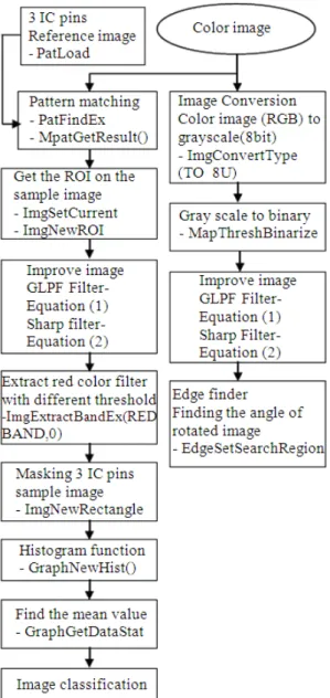
This involves specifically computer vision that will be used to detect the PCB boards flux defects during “After Cleaning” process in real time. Firstly, the introduction and then followed by methodology use and specifically highlight the algorithms used, which involved pattern matching technique. This algorithm was applied also with red color filter band (RGB) segmentation after image pre-processing to remove noise/threshold/masking. The results obtained will be presented, thoroughly discussed and conclusion will be drawn.
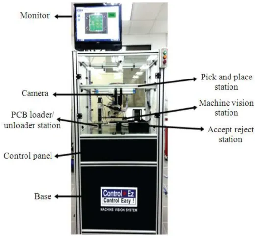
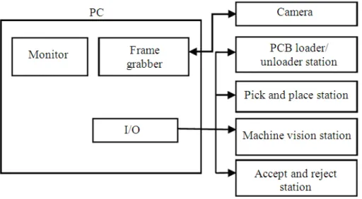
The automated modules of the machine vision system for the detection of the PCB boards flux defects are SAMSUNG camera, Matrox frame grabber and software, Dell computer, Advantech DAQ and
mechanical handler with electro-pneumatic system. The machine vision constructed with these componenets is shown in Fig. 1 along with block diagram of inspection system in Fig. 2.
2.1. Camera Specification
Crystal clear color images at 600 TV lines resolution, Ultra low light level of 0.05 Lux and 2D/3D Filtering noise reduction technology SSNRIII.
2.2. Frame Grabber Specification
Standard analog color/monochrome PCI frame grabber with two video decoders, analog composite (CVBS) or Y/C NTSC/PAL video input through BNC connectors, horizontal and/or vertical flip, sub sampling to 1/16th of a field or frame.
2.3. Computer Specification
3rd Gen INTEL® CORE™ i5-3330 processor 8GB DDR3 SDRAM, 1600 MHz -2×4 GB, 3.5” 1TB 7200 RPM SATA Hard Drive, 1X1TB.
Fig. 2. Inspection System Block Diagram
2.4. DAQ Specification
48 TTL digital I/O lines, Emulates mode 0 of 8255 PPI, Buffered circuits for higher driving capacity than 8255, Interrupt handling, Timer/Counter interrupt capability, supports both dry and wet contact and compatible with USB 2.0.
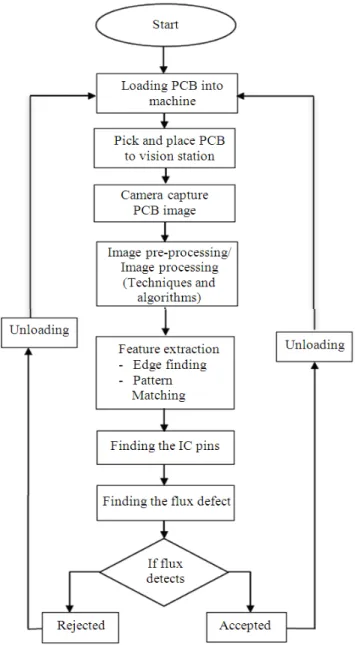
The PC-Based Machine technology also gives more advantage on control system and provides capability on the statistic database result on the product analysis compare to PLC control system. The machine will be designed and fabricated with the total automation control system with mechanical PCB loader/un-loader, pneumatic system handler with vacuum cap, vision inspection station and final electro-pneumatic classification station (accept or reject). The flowchart of PCB inspection system shown in Fig. 3 provides a clear understanding of the image processing. In this industry research, Auto Focus (AF) Lens was used where the brightness automatically detects environmental lighting to control the best light source of the illumination to the machine vision system on PCB boards inspection.
Basically, a PCB is picked from a stacker using a vacuum cup and placed on a platform. The platform moves until the PCB is directly underneath a camera, which captures an image of the PCB and sends it to the computer for processing. The results of the inspection are shown on a monitor. The inspected PCB is then placed at its respective position based on whether it is good or has errors.
The basic principle of machine vision system can be divided into few parts as below.
2.5. Image Acquisition
An optical system gathers an image, which is then converted to a digital format and stored into the computer memory.
2.6. Image Pre-Processing
GLPF and Morphology Analysis (Area Open) algorithms are used to enhance elements or remove noise off the image that are of specific importance to the process.
2.7. Feature Extraction (Image Processing)
The processor identifies and quantifies critical features in the image (e.g., PCB flux defects, pattern matching, red color filter band, threshold and histogram) and sends the data to a control program.
2.8. Decision and Control
The processor’s control program makes decisions based upon the data. Is the flux area within specification?
2.9. Detection Algorithm
2.9.1. Image Pre-Processing
The purpose of image pre-processing is to improve or to enhance the digital images. It is important for correction of geometric distortions, removal of noise, grey level correction and correction for blurring. In order to remove unwanted noise the GLPF and Morphology Analysis (Area Open) was used. As the image operations have been changed, so as the image pre-process flow chart shown in Fig. 4.
Fig. 3. Flow chart of PCB inspection system
Fig. 4. Image pre-processing
In order to eliminate the unwanted label in the ROIs area open operation was used. Area open and close operations can be used to eliminate the salt and pepper noise in the image. So what was done was that the unwanted pixels were considered as a salt and pepper noise. One can understand the working of Area open and Area close if we think an image is like a topographic surface with hills and valleys. The value of each pixel represents a certain height (with lowest pixel value darkest pixel, with highest pixel value the brightest pixel). So when area open is applied it clips the peaks of the hills until it has a plateau with an area equal to or greater than the specified minimum area. If
an area size never occurs, the peak will be clipped until all the pixels have same intensity value as the background pixel.
To increase the processing speed and reading better result of the PCB board rotated angle, the amount of information was reduced by converting color image to 8-bit unsigned grayscale, Fig. 5. In order to remove the image noise and reduce detail levels and to enhance the image structures the Gaussian Low-Pass Filter (GLPF) smoothing operator for two dimensions as in Equation 1 was applied:
2 2 2 2 2 2 (u v ) 2 (u v ) R 1 C 1 2 u,v u 0 v 0 e G1(u,v) G1 e − + σ − + − = σ = = =
∑ ∑
(1)After image smoothening with GLPF, the image will then increase its brightness for the purpose of next image processing and analysis. The brightness operation of the GLPF image was done using the Equation 2: R 1 C 1 u , v u 0 v 0 G1* a(R * C) G2(u, v) G1 − = = = =
∑ ∑
(2)2.10. Feature Extraction
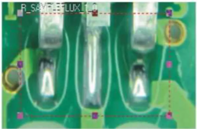
In this study, the reference image ROI (regions of interest) with the size 869×469 pixels were chosen as shown in Fig. 6 from PCB image with size 1890×2332.
After the Pre-processing stage, the image will be process with feature extraction algorithm. The purpose of the feature extraction is to segmentation the flux defect area with reference to the 3 IC’s pin. The flux defect areas always appear around the pin area instead of other parts in PCB. The red color band will be extracted from RGB color to find the flux coverage area.
The detail on the feature extraction and image processing based on pattern matching and red color filter band was shown on Fig. 7-Image Processing Algorithm.
2.11. The Pattern Matching
Function of the Pattern Matching module is to search for occurrences of a pattern in an image.
Normalized correlation operation can be seen as a form of convolution, where the pattern matching model is analogous to the convolution kernel. Ordinary correlation is exactly the same as a convolution Equation 3:
i N i i IiMi R I M = =
∑
(3)The N pixels of the model are multiplied by the N underlying image pixels and these products are summed. Note, the model does not have to be rectangular because it can contain “don’t care” pixels that are completely ignored during the calculation. When the correlation function is evaluated at every pixel in the sample image, the locations where the result is largest are those where the surrounding image is most similar to the model. The search algorithm then has to locate these peaks in the correlation result and return their positions (Where I image and M is model pixel).
Unfortunately, with ordinary correlation, the result increases if the image gets brighter. In fact, the function reaches a maximum when the image is uniformly white, even though at this point it no longer looks like the model. The solution is to use a more complex, normalized version of the correlation.
Fig. 5. The rotated image (with flux defect) and image Converted to 8-bit unsigned grayscale
Fig. 6. The ROI on the reference image where pattern matching search model for 3 IC’s pin
Fig. 7. Image processing algorithm
Function (the subscripts have been removed for clarity, but the summation is still over the N model pixels that are not “don’t care”) Equation 4:
2 2 2 2 N IM I M R [N I ( I )][N M ( M) ] − = − − ∑
∑
∑ ∑
∑
∑
∑
(4)With this expression, the result is unaffected by linear changes (constant gain and offset) in the image or model pixel values. The result reaches its maximum value of 1 where the image and model match exactly, gives 0 where the model and image are
uncorrelated and is negative where the similarity is less than might be expected by chance.
In this case, negative values are not important, so results are clipped to 0. In addition the r2 value is used instead of r to avoid the slow square-root operation. Finally, the result is converted to a percentage, where 100% represents a perfect match. So, the match score returned is actually:
Score = max(r, 0)2 x 100%
Note, some of the terms in the normalized correlation function depend only on the model and hence can be evaluated once and for all when the model is defined. The only terms that need to be calculated during the search are Equation 5:
2 I, I , IM
∑ ∑ ∑
(5)This amounts to two multiplications and three additions for each model pixel.
The sums used to compute the correlation function can be retrieved using MpatGetResult(). The retrievable sums are the following Eqation 6:
2 2
I, I , IM, M, M
∑ ∑ ∑
∑ ∑
(6) The number of pixels N is also available using MpatGetResult(). The above sums are only available if they are saved in the result buffer using MpatSetSearchParameter() with M_SAVE_SUMS set to M_ENABLE. These sums can be used, for example, to assess the model or target intensity level and contrast. Note that the correlation function calculated with the retrieved sums, will probably differ from the score returned by MpatGetResult().Although the score is derived from the correlation function, it also depends on the first and last subsampling levels chosen, optimization schemes and sub-pixel interpolation. On a typical computer, the multiplications alone account for most of the computation time.
2.12. Real Color Filter Band Algorithm
After the sample images PCB flux area are being captured by pattern matching. Then, extract the ROI to RED color filter band in a new window as shown at
Fig. 8. Adding masks to the IC component pins to
9-11 shows only flux by masking out the component’s
pins with different Threshold value. The Threshold value 100 is chosen because it produces the best result appearance to extract the flux out of 50 samples. It is supposed that the image f(x,y) consists of light objects on a dark background. One obvious way of extract the objects from the background is to select a threshold T; the threshold image F(x,y) is defined as (7):
255 f (x, y) T F(x, y) 0 f (x, y) T > = <= (7)
The images show the red color filter band with three different Threshold value (T).
For each image the histogram function is used to identify the mean value of RED intensities in the image. Only the mean value of the Red color filter band in histogram was considered to get the average on the red value pixel.
Fig. 8. The extracted image (RED-Band)
Fig. 9. T = 140
Fig. 10. T = 100
Fig. 11. T = 120
Fig. 12. The ROI (RED-Band) of the image with flux along with histogram
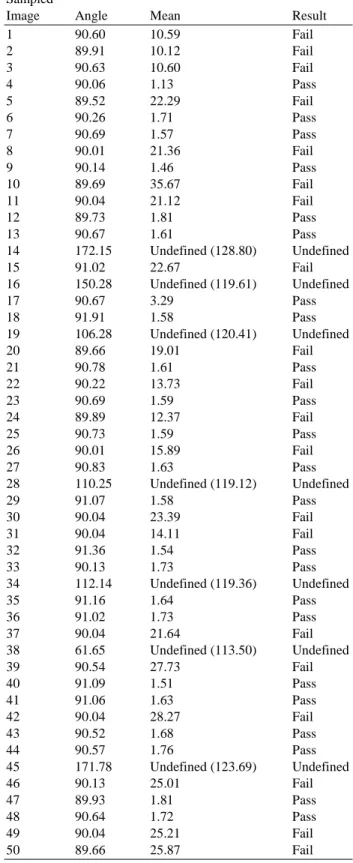
Table 1. The ROI (RED-Band) of the sample images with mean value
PCB rotated angle
Image Histogram Edge Mean Result
90.60 10.59 Fail
89.91 10.12 Fail
90.06 1.13 Pass
Repeating the same process for the sample image without the flux (pass). Note that from the Table 1 the mean value for the sample image 3 without the flux is 1.13 and the sample image 1 with the flux is 10.59. From this we conclude that if the image has a mean value over 9 then it’s considered as Fail. The histogram for ROI (RED-Band) and mean value is given at Fig. 12.
3. RESULTS
In order to test the prototype system, the pictures were taken in the real condition lighting at site. In total, 50 PCB were collected and tested with the different feature extraction technique described previously. In this research, the fix threshold is used based on Red color filter band method on histogram.
4. DISSCUSSION
After applying pre-image processing to remove the image noise and reduce detail levels and to enhance the image structures with Gaussian low-pass filter (GLPF) for smoothing. The images are ready for features extraction with pattern matching and red color filter band for PCB flux detection. Before the image processing start on the production samples, the PCB reference image or model source image will be used with the pattern matching technique to recognize the 3 IC’s pin lead for the flux area inspection. After the 3 pin lead recognition, all leads will be mask so that the balance area only contains the flux affected area for flux inspection.
In RGB representation, colors are described with three numbers for the red, green and blue components, Therefore, red filter band is applied, only the red portion in the image will be remain. Therefore, a more apparent trend of the histogram for each category due to flux defects area is given.
Table 2. Image numbers and red color filter band mean value Sampled
Image Angle Mean Result
1 90.60 10.59 Fail 2 89.91 10.12 Fail 3 90.63 10.60 Fail 4 90.06 1.13 Pass 5 89.52 22.29 Fail 6 90.26 1.71 Pass 7 90.69 1.57 Pass 8 90.01 21.36 Fail 9 90.14 1.46 Pass 10 89.69 35.67 Fail 11 90.04 21.12 Fail 12 89.73 1.81 Pass 13 90.67 1.61 Pass 14 172.15 Undefined (128.80) Undefined 15 91.02 22.67 Fail 16 150.28 Undefined (119.61) Undefined 17 90.67 3.29 Pass 18 91.91 1.58 Pass 19 106.28 Undefined (120.41) Undefined 20 89.66 19.01 Fail 21 90.78 1.61 Pass 22 90.22 13.73 Fail 23 90.69 1.59 Pass 24 89.89 12.37 Fail 25 90.73 1.59 Pass 26 90.01 15.89 Fail 27 90.83 1.63 Pass 28 110.25 Undefined (119.12) Undefined 29 91.07 1.58 Pass 30 90.04 23.39 Fail 31 90.04 14.11 Fail 32 91.36 1.54 Pass 33 90.13 1.73 Pass 34 112.14 Undefined (119.36) Undefined 35 91.16 1.64 Pass 36 91.02 1.73 Pass 37 90.04 21.64 Fail 38 61.65 Undefined (113.50) Undefined 39 90.54 27.73 Fail 40 91.09 1.51 Pass 41 91.06 1.63 Pass 42 90.04 28.27 Fail 43 90.52 1.68 Pass 44 90.57 1.76 Pass 45 171.78 Undefined (123.69) Undefined 46 90.13 25.01 Fail 47 89.93 1.81 Pass 48 90.64 1.72 Pass 49 90.04 25.21 Fail 50 89.66 25.87 Fail
The function extract only the R of RGB analysis to process the image because the PCB flux is more depend on red color only.
Fig. 13. Sampled Image and red color filter band Histogram mean value
Fig. 14. Image classification accuracy
Table 2 and Fig. 13 show the result on the red
color filter band mean value based on PCB board rotated angle. Some bigger rotated angle shows “undefined”. The reason is the pattern matching techniques used may not able to detect the flux defect after certain bigger rotation angle on the PCB. 7 out of 50 sample images cannot be classified by using this algorithm.
Figure 14 shows 86.0% accuracy with algorithm
applied.
5. CONCLUSION
This research shows that machine vision system is able to implement the sorting on PCB boards flux defects based on shape (pattern) and color space with machine vision processing. The system was developed with various images processing techniques by using Matrox Imaging software. The algorithms shown below were carried out in this research to improve the PCB fluxes defects grade into accept or reject:
• With features extraction color space based on red color filter band constraints manage to extract the PCB flux defect images
• Fix threshold can select its desire and best threshold value 100 from the image and is able to take care of different category to make sure PCB fluxes occur for the rejection category
• The feature extraction algorithm using pattern matching based on RGB color with red color filter band, having accuracy 86.0% were correctly classified
• Additional algorithm may be used to resolve the bigger PCB rotated angle
6. REFERENCES
Bhardwaj, S.C., 2012. Machine vision algorithm for PCB parameters inspection. Proceedings on National Conference on Future Aspects of Artificial intelligence in Industrial Automation, (FAAIIA’ 12), Foundation of Computer Science, New York, USA., pp: 20-24.
Chuhan, A.P.S. and S.C. Bhardwaj, 2011. Detection of bare PCB defects by image subtraction method using machine vision. Proceedings of the World Congress on Engineering, Jul. 6-8, London, UK. Greenberg, A., G. Gutarts, A. Yaari, M. Barel and J.
Nadivi, 2006. Method for printed circuit board inspection. Patent Application Publication US 2001/0002935AI.
Kaushik, S. and J. Ashraf, 2012. Automatic PCB defect detection using image subtraction method. Int. J. Comput. Sci. Netw.
Leta, F.R.,F.F. Feliciano, I.L. de Souza and E. Cataldo, 2005. Discussing accuracy in an automatic measurement system using computer vision techniques. Proceedings of the 18th International Congress of Mechanical Engineering, Nov. 6-11, ABCM, Ouro Preto, MG.
Mar, N.S.S., C. Fookes and P.K. Yarlagadda, 2009. Design of automatic vision-based inspection system for solder joint segmentation. J. Ach. Mater. Manufact. Eng., 34: 145-151.
Mashohor, S., J.R. Evans and T. Arslan, 2004. Genetic algorithm based Printed Circuit Board (PCB) inspection system. Proceedings of the IEEE International Symposium Consumer Electronics, Sept. 1-3, IEEE Xplore Press, pp: 519-522. DOI: 10.1109/ISCE.2004.1376000
Singh, S. and M. Bharti, 2012. Image processing based automatic visual inspection system for PCBs. ISOR J. Eng., 2: 1451-1455.
Sundaraj, K., 2009. PCB Inspection for missing or misaligned components using background subtraction. WSEAS Trans. Inform. Sci. Appli., 6: 778-787.
Tsai, D.M. and Y.H. Tsai, 2002. Rotation-invariant pattern matching with color ring-projection. Patt. Recogn., 35: 131-141. DOI: 10.1016/S0031-3203(00)00180-1
Zeng, Z., L. Ma and M. Suwa, 2011. Algorithm of locating PCB components based on colour distribution of solder joints. Int. J. Adv. Manufact. Technol., 53: 601-614. DOI:10.1007/s00170-010-2850-9