ENGE 311
Laboratory 5
Depletion-Layer Capacitance of a pn-Junction
OBJECTIVE
This is an experiment to investigate the depletion-layer capacitive properties of a pn-junction diode. In this experiment you will observe the bias-voltage dependent nature of the depletion-layer capacitance of the pn-junction. This junction capacitance is denoted as Cj.
SYNOPSIS
From lecture and your text reading you have observed that the depletion layer between the n- and p-sides of a diode serves as an insulating region that separates the two diode contacts. It follows that the diode in reverse bias exhibits a depletion-layer (junction) capacitance.
Hence, the pn-junction depletion-layer resembles a pair of parallel plates of area A, separation W, and electrical permittivity Si (Si = 11.70 = 11.7 8.85 10–14 F/cm = 1.04 10–12 F/cm; note that 11.7 is the relative permittivity of silicon and represents the extent to which this material concentrates electrostatic lines of flux).
This pn-junction capacitance is modeled by the relation:
Cj=εSiA W
Observe, however, that the width of the pn-junction depletion-layer is not constant; operated in reverse-bias the depletion-layer width W widens with increasing reverse bias voltage VR.
Capacitance therefore decreases accordingly – the junction serves as a voltage-controlled capacitor.
This phenomenon is modeled by:
W(V)=
(
V0−V)
1/2(
2εSiq
)
1/2
(
NA+NDNAND
)
1/2
This is effectively Eq. (3.31) (p. 147) of your text; I have re-written it in a format that is more conducive to this experiment. Recall from Lecture 14 that V0 is the built-in barrier potential of the diode and is a constant. NA and ND are the p- and n-side doping concentrations, respectively
The junction (depletion) capacitance then becomes:
Cj(V)=A
[
(
q εSi 2)
(
NAND NA+ND
)
]
1/2
¿
It stands to reason that Cj (V) only holds if the applied DC voltage V causes the diode to be
reversed-biased. (Why do you suppose this is so? You will need to justify this in your lab report.)
This equation can be re-written as:
1 C2j(V)
=k
(
V0−V)
Where:
k=
(
NA+ND NAND)(
2 q εSiA2
)
A plot of 1/Cj 2
(ordinate) vs. V (abscissa, as measured in lab) should yield a straight line for an ideal abruptpn-junction; this may also be referred to as a “doping profile.”
YOUR EXPERIMENTAL TASK
In this lab you will be experimenting with a circuit designed to measure the junction capacitance Cjas a function of the reverse-biased voltage V across the device (henceforth, V will be
designated as VR). The reverse-biased constraints you will put on your circuit is that VR will vary
from –20 V to 0 V DC.
You will need to keep the following factors in mind as you perform this experiment:
1. Typical diode junction capacitances are very small (100 pF); your test circuit has been designed to measure such a small capacitance.
2. High frequencies will be used (you will need to justify this in your lab report).
3. Circuit wires will always add some stray capacitances to your measurements; keep this in mind and use the shortest and fewest wires as possible.
MODELING A CONVIENENT CONTROLLING CIRCUIT PARAMETER
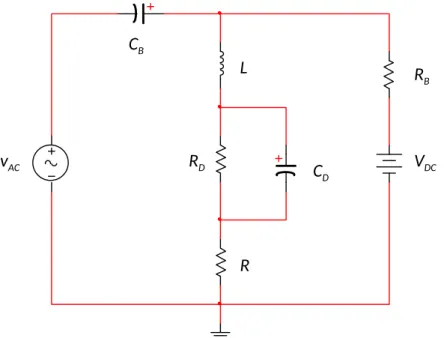
Consider the following circuit (Fig. 1) containing a parallel resistive-capacitive model of your pn-junction diode.
Fig. 1. Preliminary experimental set-up with the diode replaced with its RDCD diode model.
From your PHYS 212 and ENGE 250 knowledge you understand that the total, equivalent impedance of the series branch containing the RLC combination is:
Zeq=R+
1
jω Cj+jωL=R+j
(
ωL− 1 ωCj)
From which resonance will occur for:
Cj= 1 (2πf)2L
Since the value of your inductor L is fixed (i.e., this value will be provided to you), the only variable is frequency – a convenient controlling parameter!
C 25µF
C2 100fF
L1
0H V1
0 Vpk 0kHz 0°
R1 470kΩ
R2
470kΩ R3
470kΩ
V2 12 V
vAC VDC
RB CB
CD RD
L
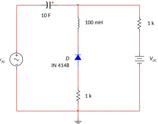
A. Pre-Lab Simulation and Experimental Set-Up
1. Your first task is to simulate the circuit in Fig. 2.
2. Using an initial estimate of 100 pF for the diode junction capacitance Cj calculate the
expected resonate frequency 2 = 1/LC
j. Use this value to choose a starting point for the
frequency of your function generator (your AC source). .
3. Power supply voltage (i.e., your DC source): Start at –20 V and measure the reverse-bias voltage drop VR across the diode. Simultaneously, measure the voltage across the resistor
R via the oscilloscope; vary the frequency until the RLCjbranch reaches resonance.
Record the resonance frequency at this value of VR.
4. Continue to repeat Step 3 above for 1 V increments of VR up to, and including 0 V. As
you get down to about –2 volts you may need to take finer voltage increments, if necessary and if possible (e.g., ¼ volt increments).
5. Tabulate your measurements from Steps 3 & 4 above and plot results for (a) Cj vs. VR;
(b) 1/C2j vs. VR.
Fig. 2. Your test circuit for pn-junction diode capacitance measurement.
C 25µF
L1
0H V1
0 Vpk 0kHz 0°
R2
470kΩ
R3 470kΩ
V2 12 V
D1 1N6096
vAC VDC
10 F
D
IN 4148
100 mH
1 k
1 k
B. Report
1. From your plot 1/Cj 2
vs. VR (the “doping profile”) estimate the slope k and the intercept
“b” and give V0. Use the relation given on p. 2:
1 C2j(V)
=k
(
V0−V)
Again, be aware that “V” in this equation represents the reverse-bias voltage VR from
Steps 3 & 4.
2. Discuss (explain) the results of your experiment, keeping your discussion concise, short, and to the point. For instance, discuss the linearity of your doping profile; what is the physical significance of the linearity?
3. Explain why the circuit constructed for this experiment was chosen for measuring diode junction capacitance. What are the reasons for the different passive components?
4. Is the experimentally determined value of the barrier voltage V0 a value that you would expect based on lecture and what you’ve been reading in your ENGE 311 text? If it isn’t within a range that you would expect, judiciously explain why this might be the case.
5. Determine the zero-bias junction capacitance CJ0 (i.e., the junction capacitance at zero