Look Ahead Clock gating using an Auto gated Flip flop for Low Power Application
Subin Raj C1, Jebasingh Kirubakaran S J2, Arulmary A3, Senthil Kumar V4
P.G Scholar, Department of ECE Vel Tech Multitech
Avadi, Chennai.India [email protected]
ABSTRACT: We propose new technique for clock gating. Clock gating is helpful for reducing power consumed in digital
systems. There are three technique used, viz., (i) Synthesis Based method (ii) Data driver Method, and (iii) Auto gated flip flop (AGFF). The Auto gated Flip flop can be distributed in the clock distribution network. Clock distribution uses current other than voltage by giving global clock. With auto gated flip flop, it is used for power sowing. Clock gating can be tested in current mode pulsed flip flop which enable urrent-Mode Pulsed Flip-Flop with Enable (CMPFFE) using 48nm CMOS technol-ogy. In the Look Ahead Clock Gating (LACG) computers, the clock signals at one cycle ahead of time. The Flip flop depends on the present cycle in LACG. This model can be characterized by power saved in FF. This technique is based on a data to clock togging. Majority of the FF fall in positive Region. Experimentation shows that the industry-scale data displays 22.5% reduction of clock power.
Keywords: Look-Ahead Clock Gating (LACG), Auto-Gated FFs (AGFF), Current-Mode Pulsed Flip-Flop with Enable (CMPFFE).
Received: 17 October 2016, Revised 19 November 2016, Accepted 28 November 2016
© 2017 DLINE. All Rights Reserved
1. Introduction
Synthesis based clock gating is used in EDA tools. The abducing clock pulses can be measured by data to clock toggling Ratio. The clock enacting signals are derived by Logic synthesis. It is shown in data toggle in very Low rate compared to the gated clocks. The clock load thus consumes more power.
In order to address data driven clock gating, the clock signal driving a FF is gated when there is no change in the clock cycle. The relation between data driver-based and synthesis-based clock gating method shown in the Arithmetic circuits. The data driver gating is explained in Fig. 1. The disabled clock can be find in the next cycle using a FF by Xoring the output with present input; then the output will display in next cycle. The output of XOR gate is OR Ed together for joint gating. Data driven gating is suffered by a short time- window. Clock gating is explained in the Fig 2 and the design methodology is very difficult in data driven method. In order to maximize the power saving, flip flop is grouped together. The main applications are unknown and the redundant clock pulses may increase in specific application. The IP providers who are delivering RIT code need to broadcast the gating circuitry as per customer. It requires marinating different version of the same IP.
Figure 1. Circuit implementation of data – driven clock gating
Figure 2. Sequencing of gating logic in data driven clock gating
In this paper, we propose Look Ahead Clock Gating (LACG). It shows clock enabling signal at each flip flop. It depends on present cycle data same as data driven gating AGFF and the data driven enable full clock signal. Data Driven requires optimization of FF. The simplified gating implementation is Auto gated Flip flop.
The Rest of the paper discussed about the optimization and implementation LACG section develops power saving models.
2. Overview of Autogated Flip Flop
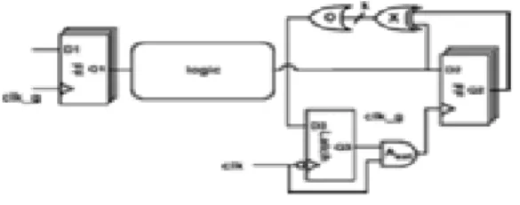
The basic circuit diagram of Autogated flip flop is shown in the figure 3. The flip flop master latches are transparent in falling edge of the clock. The output must be stable. When master latch is opaque, then EXOR gate shows batch change in state.
Figure 3. A gated flip-flop
LACG uses AGFF for three goals. In order to stop the clock pulses in master Latch, and making the clock pulse applicable for general design and avoiding timing constraints LACG is based on XOR output. The XOR output is valid only during a narrow window [-t setup, tccq] where t is setup and tccq are FF’s are setup time. If tccq delay the XOR output and turns to zero, XOR and OR gate are helpful in clock switching.
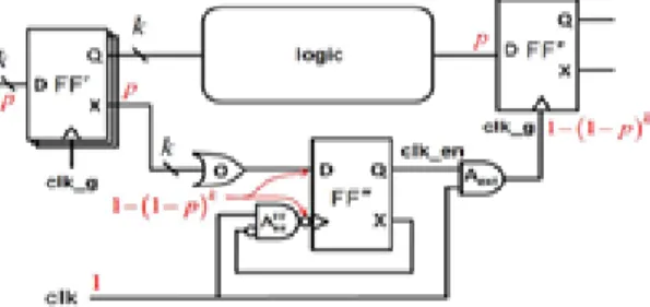
Figure 4 represents how LACC operators assume FF11 as target and FF1 as source. The target depends on K ≥ 1of source FF’s. The source FFs can be found by a transversal of the Logic paths for D11. It performs RTL or NOT-list description.
Figure 4. LACG of general logic
Generate the enable signal obtained from t and its validity is t +1. The clock edge falling ad t +0.5 then D111 (t+0.5) = ∑
×(o11)x(t) since FF111 is opposite to clock. The signal Q111 is stable when the time period is [t + 0.5, t +1]. By using FF for gating, the
consumption of power will be its own. In figure 4 identity that FF111 is clocked oppositely. Here internal XOR gate will be
connected between D111 and Q 111. LACG has a full clock cycle in order to evaluate clock. For implementation, require clock
enabling signal. LACGs are derived from the figure 5.
Figure 5. Timing sequence of LACG clock gating
Where tpdq, txand tALatch are output propagation delay, t
setup and FF is setup time.
t0 + t setup fp + tpcq-ff + t Aext < Tc+tx+tAintLatch (2)
There equation 2 is independent of timing circuit. The clock enabling signal is propagated from t setup – FF time window. As mentioned earlier ∑x(D11)×(t) = 0 is sufficient clock. the D11 can be evaluated and then D11 (t+1) = D11 (t). There will be a question have large.
Pr[(D11(t+1) = D11(t)Λ(∑x(D11× (t)=1)]
Thus LACG is power savor analyzed by worst-case toggling independence model from the theoretical approval where power saving is analyzed.
3. Methodology of Power Saving
The current mode signalling scheme perform current to voltage and obtain voltage mode clock signal current mode is integrated if it directly consumes CM signal in order to reduce power consumption. The clock gating can be implemented into the current model signaling shown in the Fig 6.
Figure 6. Previous CM schemes used an expensive transmpedance amp Rx which could in significant skew due to Vcm Shift if applied to CDNs
Current mode pulsed flip flop with Enable is the advance technology in current mode, CMPFFE perform well other than CM signaling. CMPFEF is similar to CM signal but here uses action low enable (EN) and if uses current-comparator. CC is a static storage call. A small signal analysis is expressed in CMPFFE.
Zin= gm1 + gm21 (3)
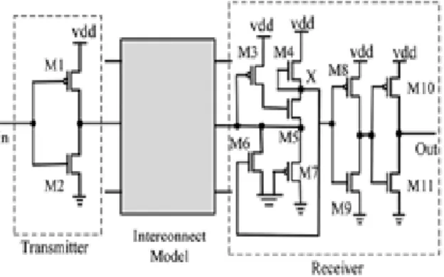
In CMPFFE, the transfer provides a push – pull current, and LACG is implemented in between CMPFFE. The transmitter receives voltage and clock signal that can be controlled by clock gating. Then, the current will distributed equally to all CMPFFE modes. In Figure 7, the transmitter circuit uses NAND – NOR design. Here, PMOS change from the supply then the NMOS will be in off state. Simultaneously NOR gate willies the negative clock, then NMOS will sink with current. While the M1 is off the PMOS get charged. Then Non- over login signal from the NAND – NOR will remove any short circuit current from transistor.
When the FF are toggled then
Pr [∑Xcd11x(t) = 0] = (1 - P)k
The Actual power obtained from the following analysis.
Figure 7. (a) The proposed CM Tx and CDN converts an VM input signal to a push – pull current with minimal interconnects voltage swing and distributes current equally to the CMPFFEs.
(b) Simulation waveforms confirm a VM input is converted to a constant CDN voltage and a represent push-pull current at each CMPFTE.
Pr = [∑Xcd11x(1) = 1Λx11 (6 + 1) = 0] = [1-(1-p)k](1-p) (5)
In order to consulate LACG consider toggling as shown in the figure 3, the target of the FF will be
{2(1-p)k - [1-(1-p)k]} Cff + CLK - Pcx = [3(1-p)k-1] Cff + CLK - Pcx (6)
3 3
Summing up all the above components, the following result will be obtained
[1-(1-p)k] cff + C
Aint + CAint + [1 = (1-p)
k + Kp] (7)
From 6 and 7 rearrangement gives
CSave
dyn = (1-p)
k (cff + clk + cff + co) - p(cx + kco) - Cff + CLK + C
Aint + cff + C0] (8) 3
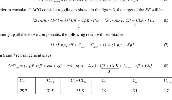
Cff CCLK Cff + CLK CY Co CAint
25-7 31.5 35-9 2.9 3.1 1.7
Table 1. Typical capacitance in 20 Nm process Technology values in 10-15 f
4. Experiments For Minimizing Logic Gates
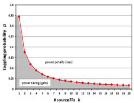
From the equation 8, CSave are decreasing with the increase of P and K substitute Csave = 0 in eqn 8 dependency between P and q from the fig 8 and from the table (1), we take 20 nm process technology library. When the (k,p) points fall in the curved LACG will loose power the capacitance measured in 10-5.
Figure 8. Power saving breakeven curve
Since the clock is driven by Automating, the efficiency of the OR logic depends on best case and worst case. In CMPFFE, input transition is 50% and output transition is 50%. The CMPFFE have lower clock – Q delay. The Monto carcoa simulation of clk-– Q delay of Autogated clock gating is shown in figure 9. The flip-flop power will not represent the overall power consumption of the current mode. Power saving can be shown in CMPFFE with total power and the additional static power.
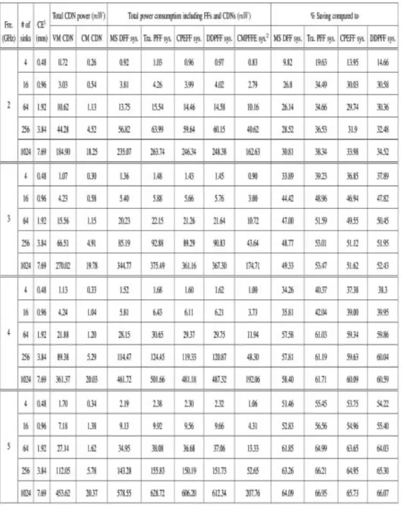
Table 2. Power Saving Description
The maximum cost perfect matching (MCPM) algorithm used to satisfy wcc(i) = 0 then the gating logic of ffi and ffj are not merged. A heuristic solution was proposed by LACG successfully.
5. Experimentation Results
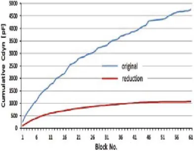
In figure 10 clock, cdyn is 4770 of which 1060 pf has been reduced by LACG total dynamic power reduction where 22% power saving is achieved only by LACG. The dynamic power depends on logic and static power independent of switching activity. The Static power is 21% of total power taking all factors into account 22% of clock cdyn reductions were translated into 12.5% reduction of total power.
Figure 10. Cumulative cdyn before gating and the amount of reduction achieved by LACG
Figure 11. Simulation of clock gating
6. Conclusion
References
[1] Ravish Khan, Athar., Gulhane, M., Padmini, G., Kaushik, Sanjay,(March 2013). Dynamic Power Reduction of Digital Circuits by Clock Gating, International Journal of Advancements in Technology, 4 (1) IJoAT.
[2] Benini, L, A., Bogliolo, A., De Micheli, G (2000). A survey on design techniques for system- level dynamic power management,
IEEE Trans.VLSI Syst., 8 (3) 299–316.
[3] Chen Farrahi, C., Srivastava, A., Sarrafzadeh, M., Tellez, G (2001). Activity driven clock design, IEEE Trans. Comput. Aided Des. Integr. Circuits Syst., 20 (6) 705–714,
[4] DeCaro, D., Napoli, E., Strollo, A.G.M. (2000). New Clock-Gating Techniques for Low-Power Flip-flops.
[5] Decaro, D., Stroll, A.G.M (2000). Low power flip-flop with clock gating on master and slave latches, Electronics Letters 36 (4). [6] Jyoti, Malay Ranjan., Tripathy, Vijeta. (2012). Comparison of Conditional Internal Activity Techniques for Low Power Consumption and High Performance Flip-Flops, International Journal of Computer Science and Telecommunications. [7] Malathi, M., Parvathi Karthica, A., Rajshekar, P., Vinoth Kumar, S (2013). Comparative analysis of clock gated data look ahead and conditional capture flip-flops and their area of Applications, International Journal of Computer Applications, National conference on VLSI and embedded systems.
[8] Mehra, Rajesh., Kaur, Upwinder (2013). Low power cmos counter using clock gated flip-flop, International Journal of Engineering and Advanced Technology (IJEAT) 2 (4).
[9] S. Wimer, S., Koren, I (2012). The Optimal fan-out of clock network for power minimization by adaptive gating, IEEE Trans. VLSI Syst., 20 (10) 1772–1780,.