Simulation of an Efficient Hybrid Transformer DC-DC
Converter for PV Based Renewable Energy Sources -Power Conditioning
Systems (PCS) Applications with High Boost Ratio
RAJENDER
P.G. scholar, Dept of EEE
Trr College of Engineering & Technology,
Hyderabad, Telangana, India
. L. MURALI KRISHNA Assistant professor, Dept of EEE
Trr College of Engineering & Technology,
Hyderabad, Telangana, India
Abstract: - With the increase in renewable energy
resources there is need for better conversion devices. as most of the renewable energy resources are low voltage devices like PV cells and fuel cells the voltage needs to be stepped up before conversion. So there is a need for high efficient dc-dc converter. In this paper a non-isolated, high boost ratio hybrid transformer dc-dc converter with applications for low voltage renewable energy sources is being proposed. The proposed converter utilizes a hybrid transformer to transfer the inductive and capacitive energy simultaneously, achieving a high boost ratio with a smaller size magnetic component. As a result of incorporating the resonant operation mode into the traditional high boost ratio PWM converter, the turn off loss of the switch is reduced, increasing the efficiency of the converter under all load conditions. The input current ripple is also reduced because of the linear-sinusoidal hybrid waveforms. The voltage stresses on the active switch and diodes are maintained at a low level and MPPT algorithm is being added to the proposed model utilizing the maximum power generated from the low voltage PV system.
I. INTRODUCTION
Renewable energy resources such as wind and solar energy are increasingly integrated in power system planning and operation to achieve emission reductions and to reduce consumption of fossil fuels by conventional thermal power generation. So integrating the power from the PV module into the existing power distribution infrastructure can be achieved through power conditioning systems (PCS). Typical PCS can be accomplished by using a single-stage or double-single-stage structures. The double-single-stage PCS, as shown in Fig. 1 [1]-[7], consists of a dc-dc conversion stage that is connected to either a low power individual inverter or a high power centralized inverter that multiple dc-dc converters could connect to. The dc-dc conversion stage of the PCS requires a high efficiency, high boost ratio to increase the low
dc input voltage from the PV panel to a higher dc voltage. This voltage has to be higher than the peak output voltage (Vac) of the inverter, nominally is in the 380V-400 V range. The high boost ratio dc-dc converter for such systems can be isolated or non-isolated; however, transformer-isolated converters tend to be less efficient and more expensive due to the increased manufacturing costs. A non-isolated dc-dc converter with a high boost ratio would be advantageous for a two-stage PCS [1] because it can be easily integrated with current PV systems while reducing the cost and maintaining a high system efficiency.
Due to the different output voltages from the PV panel it would be beneficial to have a PCS with a high efficiency over the entire PV voltage range to maximize the use of the PV during different operating conditions. Another important function of the dc-dc converter for PV applications is being able to implement maximum power point tracking (MPPT). The ability to implement MPPT for an individual PV panel would ensure that a large cluster of PV could maintain maximum power output from each panel without interfering with the other panels in the system. The major consideration for the main power stage of the converter in being able to implement an accurate MPPT is that the input current ripple of the converter has to be low
Of the high boost ratio non-isolated dc-dc converter topologies published [7]-[19], the use of coupled-inductor and switched-capacitor is attractive because only a single low voltage active switch is required for such type of topologies. The reason that the primary side active switches of the high boost ratio converters have low voltage stress is because of the transformer effect from the coupled-inductors. Since there is a low voltage stress on the active switch the circuit can then use low voltage MOSFETs that generally have a low ( ) and smaller switching periods, decreasing both the conduction and switching losses. An earlier paper on high boost ratio non-isolated dc-dc converter [8] presented a clamp-mode couple-inductor buck-boost converter. The converter’s leakage energy from the coupled-inductor was recycled reducing the turn off switching loss and voltage stress of the main switch. However, the output diode stress was similar to that of a traditional flyback converter, i.e. higher than the output dc bus voltage. Another drawback of the converter was that there was a high input current ripple due to the fact that there was no direct energy transfer path when the MOSFET is off. Further improvements in increasing the boost ratio of a simple dc-dc converter were accomplished by combining a boost converter with a flyback converter [9], [10]. Compared with the converter in [8], the boost ratio was improved as a result of the outputs of the boost converter and flyback converter being connected in series; however, the same issues that affected the converter in [8] remained. By adding a switched-capacitor in series with the energy transformer path, a new improved high boost ratio dc-dc converter with coupled-inductor and switched-capacitor [11] was introduced.
A switched-capacitor was inserted between the primary side and secondary side of the coupled
the output diode stress closer to that of the output dc bus voltage. However, the magnetic core was not fully utilized because the magnetic core functioned more as an inductor than as a transformer. Light load efficiency of the converter is also reduced because switching losses were more dominant under light load conditions. For application such as PV module converter, the high efficiency over a wide load range is extremely important because the performance is weighted differently for specific load levels in the California Energy Commission (CEC) standards.
In this paper, a hybrid transformer is presented to get the high boost ratio of dc-dc converter. By adding a small resonant inductor and reducing the capacitance of the switched capacitor in the energy transfer path, a hybrid operation mode [20], [21], which combines PWM and resonant power conversion, is introduced in the proposed high boost ratio converter. The inductive and capacitive energy can be transferred simultaneously to the high voltage dc bus increasing the total power delivered decreasing the losses in the circuit. As a result of the energy transferred through the hybrid transformer that combined the modes where the transformer operates under normal conditions and where it operates as a coupled inductor, the magnetic core can be used more effectively
The continuous input current of the converter causes a smaller current ripple than that of previous high boost ratio converter topologies that used coupled-inductors. The lower input current ripple is useful in that the input capacitance can be reduced and it is easier to implement a more accurate MPPT for PV modules. The conduction loss in the transformer is greatly reduced because of the reduced input current RMS value through the primary side. The voltage stress of the active switch is always at a low voltage level and independent of the input voltages. Due to the introduction of the resonant portion of the current, the turn off current of the active switch is reduced. As the result of the decreased RMS current value and smaller turn off current of the active switch, high efficiency can be maintained at light output power level and low input voltage operation. Because of the resonant capacitor transferring energy to the output of the converter, all the voltage stresses of the diodes are kept under the output dc bus voltage and independent of the input voltage.
Fig.2. Proposed high boost ratio dc-dc converter with hybrid
Fig.2 shows the circuit diagram of the proposed converter. is the input capacitor; HT is the hybrid Transformer with the turn ratios 1: n; M1is the active MOSFET switch; D2 is the clamped diode, which provides a current path for the leakage inductance of the hybrid transformer when M1is off; Cr2captures the leakage energy from the hybrid transformer HT and transfers it to the capacitor Cr1 by means of a resonant circuit composed of Cr1, Cr2, and D1; is a resonant inductor, which operates in the resonant mode; D1is a diode used to provide a unidirectional current flow path for the operation of the resonant portion of the circuit. Cr1 is a resonant capacitor, which operates in the hybrid mode by having a resonant sinusoidal charge and PWM linear discharge. The turn on of D1is determined by the state of the active switch M1.D3is the output diode similar to the traditional coupled-inductor boost converter; Cois the output capacitor.
A. Converter Operation
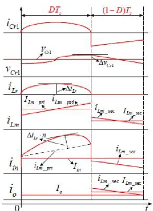
Fig.3 illustrates the five steady state topology stages of the proposed dc-dc converter for one switching cycle. Fig.4 shows the key voltage and current waveforms for specific components of the converter over the switching cycle. For the waveforms represented in Fig.4, g1 represents the driver signal for the active MOSFET switch M1; is1is the current of the MOSFET M1; iCr1is the current of the resonant capacitor Cr1; iCr2 is the current of clamped capacitor Cr2; is the primary side current of hybrid transformer HT; is the current of the output diode; vs1and vD3are the voltage waveforms of the active switch MOSFET M1and the output diode D3respectively. For simplicity of analysis, we assume that the dc input voltage is a stiff voltage source with a constant voltage and all the switch and diodes are ideal devices.
The five operation modes are briefly described as follows.
[Fig.3(a)]: [t0,t1], In this period, MOSFET M1 is on, the magnetizing inductor of the hybrid transformer is charged by input voltage, while Cr1 is charged by Cr2 and the input voltage Vin together by the resonant circuit composed of secondary side of the hybrid transformer HT, Cr1 , Cr2, Lr and D1. The energy captured by Cr2 is transferred to Cr1, which in turn is transferred to the load during the off time of the MOSFET. The current in MOSFET M1 is the sum of the resonant current and linear magnetizing inductor current as shown in fig. 4. There are two distinctive benefits that can be achieved by the linear and resonant hybrid mode operation. The first benefit is that the energy is delivered from source with the capacitive mode and inductive mode simultaneously. Compared to previous coupled-inductor high boost ratio dc-dc converters with only inductive energy delivery, the dc current bias is greatly reduced, decreasing the size of the magnetic. Second the turn-off current is decreased; this causes a reduction in the turn-off switching losses.
[Fig.3(c)]: [t2, t3], At time t2, the capacitor Cr2 is charged to the point that the output diode D3 is forwarded-biased. The energy stored in the magnetizing inductor and capacitor Cr1 is being transferred to the load and the clamp diode D2 continues to conduct while Cr2 remains charged.
[Fig.3(d)]: [t3, t4] At time t3, diode D1 is reversed-biased and as a result, the energy stored in magnetizing inductor of the hybrid transformer and in capacitor Cr1 is simultaneously transferred to the load. During the steady state operation, the charge through capacitor Cr1 must satisfy charge balance. The key waveform of the capacitor Cr1 current shows that the capacitor operates at a hybrid switching mode, i.e., charged in resonant style and discharged in linear style.
[Fig. 3(e)]: [t4, t0], The MOSFET M1 is turned on at time t4. Due to the leakage effect of the hybrid transformer, the output diode current will continue to flow for a short time and the output diode D3 will be reversed-biased at time t0 then the next switching cycle starts
: Hybrid Transformer : Active MOSFET Switch
: Resonant Capacitor : Resonant Inductor
: Resonant Diode : Clamp Diode
: Clamp Capacitor : Output Diode
The boost ratio Mbcan be obtained by three flux balance criteria for the steady state. The first flux balance on the magnetizing inductor of hybrid transformer requires that in steady state
=
(1)
Second, according to flux balance on the resonant inductor during ON time
=
+
=
+
(2)
The last flux balance that governs the circuit is voltage second balance of the magnetizing inductor in the hybrid transformer for the whole switching period
=
( )(1 + )
(3)
By substituting equation (2) into equation (3), the boost conversion ratio can be obtained=
=
(4)
The conversion ratio is similar to the conventional boost converter except that the turns ratio term n is added, so the traditional duty ratio control method that is applied for a standard boost converter can also be applied to the onverter.
B. Voltage Stresses of the Switches
Voltage stresses for all switches are determined in this section to select power devices with the proper rating and all the results are respect to the output dc voltage. From the circuit diagram of t0 to t1and t1 to t2in fig. 3 respectively, the voltage stresses for MOSFET M1 and clamped D1 are obtained
Fig.4. Key waveforms for different operation modes
From the circuit diagram of t0to t1and t2to t3in Fig. 3, one obtains the voltage stress of diode D2 and output diode D3
=
=
−
=
− 1 −
=
( )(6)
From equation (5) and equation (6), it is obvious that all the voltage stresses of the switches are independent of input voltage and load conditions. In other words, all the voltage stresses of the switches are optimized based on the output voltage and the turns ratio of the transformer. The resonant period
Tr and resonant frequency are given by
T = 2π√l c (7)
f = (8)
If the constant on time control Ton is used, choose Ton=1/2Tr so that the resonant diode can turn off at zero-current condition and conduction loss can be minimized. In the experimental implementation of the hybrid transformer, the leakage inductance of the
hybrid transformer should be considered, so the total resonant inductance is expressed as follows
L; = L + L +n L (9)
Where, L is the secondary side leakage inductance andL is the primary side inductance of the hybrid transformer. The resonant capacitance Cr is composed by Cr1 and Cr2 in series. Normally, we choose ≪ so voltage stress of the MOSFET can be clamped well. The optimal operation mode is the constant PWM on time Ton control with variable frequency, however traditional PWM control method is applicable to the proposed converter as described in [20], [21].
C. Analysis of energy transfer
The simplified waveforms for energy transfer analysis are shown in Fig. 5. In order to analyze the energy transfer feature from the low voltage dc energy source to the high voltage dc bus, it is necessary to solve the equivalent circuit in fig. 3 (a) subject to the initial conditions imposed by the previous PWM OFF- time interval given by
i (0) = 0 (10)
V (o) = −∆V (11)
where∆v is the ripple of the resonant capacitor Cr1. The resonant solution is obtained as
V (t) = ∆V cos 2πf . t (13)
∆V = R . ∆i (14)
whereR is characteristic impedance given by
R = √L c (15)
For PWM off time interval, the discharge equations of the resonant capacitor Cr1 are given by
∆V = _ (16)
I _ = = (17)
Where ILm_sec is the average linear magnetizing current referred to secondary side of the hybrid transformer, Io is the average output current, Po is the output power andVois the output voltage
From equations (14), (15), (16) and (17), the relationship between and linear magnetizing current and sinusoidal resonant current can be expressed as
∆i = π. f . T . I _ . (1 − D)
Fig.5. Waveforms for energy transfer analysis
Accordingly, the average primary side sinusoidal resonant current of hybrid transformer is given by:
I _ = n. ∆i (19)
Substituting equation (18) into equation (19) yields:
I _ = = n. f . T . I (20)
The average input current can be obtained from equation (4) by power balance
=
.
(21)
For the optimal mode operation, the relationship between the resonant frequency and the switching period is
=
. .(22)
Substituting equation (22) into equation (20) yields:
_
=
.(23)
The resonant contribution index of energy transfer by sinusoidal resonant current can be defined as the ratio between the input average resonant current
_ to the total input current
K = II_ = nI2D 1 − D In + 2
= . = . (24)
In order to optimize the operation of the proposed converter, needs to be increased, this will reduce the turn off losses of the MOSFET and decrease the size of the magnetic core used.
III. S
IMULATIONR
ESULTSIn order to verify the effectiveness of the proposed converter, a SIMULINK model is being developed in MATLAB shown in fig:6
Fig. 6: SIMULINK model of proposed system
The proposed system consists of a low voltage PV system , MPPT, high boost ratio hybrid transformer dc-dc converter as dc-dc converter can increase the efficiency up to 97%with MPPT total utilization of input power is possible .with MPPT fast adjustments of voltages is possible where the maximum power could be achieved .
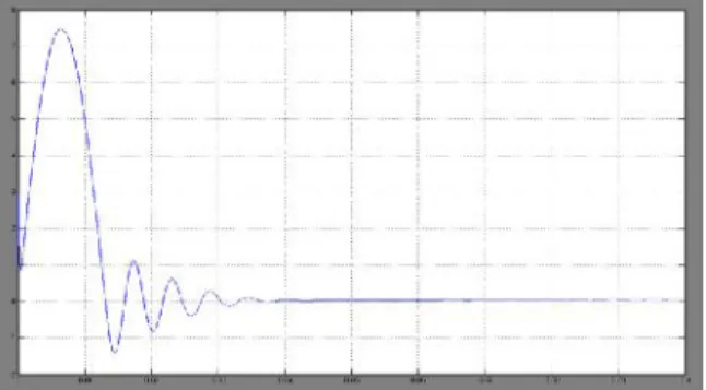
As fig 7 shows the output voltage of the system when the PV system is being connected to the dc-dc converter through the MPPT block. From the fig we can observe the reduction in voltage variation achieved through high boost ratio dc-dc converter hybrid transformer.
Figure 8 shows the output voltage of a MPPT
IV. CONCLUSIONS
In this paper dc-dc converter hybrid transformer with high boost ratio suitable for alternative dc energy sources with low dc voltage input is proposed in this paper. with the operation of dc-dc converter with coupled-inductor and switched capacitor has benefits as the converter transfers the capacitive and inductive energy simultaneously to increase the total power delivery reducing losses in the system. And the conduction loss in the transformer and MOSFET are reduced as a result of the low input RMS current and switching loss is reduced with a lower turn off current. With these improved performances the converter can maintain high efficiency under low output power and low input voltage conditions. With the proposed model an uplift in voltage with less distortion is being simulated in the paper
REFERENCES
[1] J.S. Lai, “Power conditioning circuit topologies,”
IEEE Ind. Electron. Mag., vol. 3, pp. 24-34. Jun.
2009.
[2] S. B. Kjaer, J. K. Pedersen, and F. Blaabjerg, “A review of single-phase grid-connected inverters for photovoltaic modules,”IEEE Trans. Ind. Appl., vol.
41, pp. 1292-1306, Sep./Oct. 2005.
[3] F. Blaabjerg, Z. Chen and S. B. Kjaer, “Power Electronics as Efficient Interface in Dispersed Power Generation Systems,”IEEE Trans. Power Electron.,
vol. 19, pp. 1184–1194, Sept. 2004.
[4] Y. Xue, L. Chang, S. B. Kjaer, J. Bordonau, and T.Shimizu, ‘‘Topologies of single-phase inverter for
small distributed power generators: An overview,’’
IEEE Trans. Power Electron., vol. 19, pp. 1305– 1314, Sept. 2004.
[5] B. Liu, S. Duan, “Photovoltaic DC-Building-Module- Based BIPV System-Concept and Design Considerations,”IEEE Trans. Power Electron., vol.
26, No. 5, pp. 1418–1429, May 2011.
[6] Q. Li and P. Wolfs, “A Review of the Single Phase Photovoltaic Module Integrated Converter Topologies with Three Different DC link Configurations,”IEEE 605 Trans. Ind. Electron., vol.
23, no. 23, pp. 1320-1333, Apr. 2008.
[7] W.H. Li and X. N. He, “Review of Non-isolated High Step-Up DC/DC Converters in Photovoltaic Grid- Connected Applications,” IEEE Trans. Ind. Electron., vol. 58, pp. 1239-1250, Apr. 2011.
[8] Q. Zhao and F.C. Lee, “High-efficiency, high stepup dc-dc converters,” IEEE Trans. Power Electron., vol.18, no. 1, pp.65-72, Jan. 2003.
[9] K. C. Tseng and T. J. Liang, “Novel high-efficiency step-up converter,” Proc. Inst. Elect. Eng.—Elect. Power Appl., vol. 151, no. 2, pp. 182– 190, Mar. 2004.
[10] T. J. Liang and K. C. Tseng, “Analysis of integrated boost-flyback step-up converter,” IEE Proc.-Electr. Power Appl., vol. 152, no. 2, pp.
217-225, Mar. 2005.
[11] R.J. Wai and R. Y. Duan, “High Step-Up Converter With Coupled-Inductor”, IEEE Trans. Power Electron., vol. 20, pp. 1025-1035, Sept. 2005.
RAJENDER REDDY TALLA currently pursuing his M.Tech in Electrical Power Systems from TRR Engineering College, Hyderabad, Telangana, India affiliated to JNTU University, Hyderabad. He has done his B.Tech degree from Ellenki College of Engineering and Technology, affiliated to JNT University, Hyderabad, Telangana, India and his fields of interest include Non Conventional Energy Sources and Power Systems.