UNDERSTANDING THE VAPOR-LIQUID-SOLID AND VAPOR-SOLID-SOLID MECHANISMS OF SI NANOWIRE GROWTH TO SYNTHETICALLY ENCODE
PRECISE NANOSCALE MORPHOLOGY
Christopher William Pinion
A dissertation submitted to the faculty at the University of North Carolina at Chapel Hill in partial fulfillment of the requirements for the degree of Doctor of Philosophy in the Department
of Chemistry in the College of Arts and Sciences.
Chapel Hill 2017
ã 2017
ABSTRACT
Christopher William Pinion: Understanding the Vapor-Liquid-Solid and Vapor-Solid-Solid Mechanism of Si Nanowire Growth to Synthetically Encode Precise Nanoscale Morphology
(Under the direction of James Cahoon)
Precise patterning of semiconductor materials utilizing top-down lithographic techniques is integral to the advanced electronics we use on a daily basis. However, continuing development of these lithographic technologies often results in the trade-off of either high cost or low throughput, and three-dimensional (3D) patterning can be difficult to achieve. Bottom-up, chemical methods to control the 3D nanoscale morphology of semiconductor nanostructures have received significant attention as a complementary technique. Semiconductor nanowires, nanoscale filaments of semiconductor material ~10-500 nm in diameter and ~1-50 microns in length, are an especially promising platform because the wire composition can be modulated during growth and the high aspect ratio, one-dimensional structure enables integration in a range of devices.
While investigating the vapor-liquid-solid mechanism, we noticed instances of unique catalyst behavior. Upon further study, we showed that it is possible to instantaneously and reversibly switch the phase of the catalyst between a liquid and superheated solid state under isothermal conditions above the eutectic temperature. The solid catalyst induces a vapor-solid-solid growth mechanism, which provides atomic-level control of dopant atoms in the nanowire.
TABLE OF CONTENTS
LIST OF FIGURES ... ix
LIST OF TABLES ... xi
LIST OF ABBREVIATIONS ... xii
CHAPTER 1: INTRODUCTION ... 1
1.1 Semiconductor Nanowires ... 1
1.2 Nanowire Synthesis ... 2
1.2.1 Vapor-Liquid-Solid Mechanism ... 2
1.2.2 Vapor-Solid-Solid Mechanism ... 3
1.3 Understanding Nanowire Growth Mechanisms ... 4
1.4 Characterizing and Modeling Nanowire Growth ... 5
1.5 Controlling Nanowire Composition ... 5
References ... 8
CHAPTER 2: SYNTHETICALLY ENCODING 10-NM MORPHOLOGY IN SILICON NANOWIRES ... 13
2.1 Introduction ... 13
2.2 Nanowire Synthesis and Etching ... 15
2.3 Optimization of ENGRAVE Technique ... 16
2.6 Detailed Methods ... 24
2.6.1 Nanowire Growth ... 24
2.6.2 Etching and Device Fabrication ... 25
2.6.3 Electron and Raman Microscopy ... 26
2.6.4 Finite-Element simulations ... 26
References ... 27
CHAPTER 3: IDENTIFYING CRYSTALLIZATION AND INCORPORATION LIMITED REGIMES DURING VAPOR-LIQUID-SOLID GROWTH OF SI NANOWIRES ... 32
3.1 Introduction ... 32
3.2 Experimental Design ... 36
3.3 Results ... 38
3.4 Kinetic Modeling ... 41
3.5 Analysis and Discussion ... 45
3.6 Conclusions ... 49
3.7 Detailed Methods ... 50
3.7.1 Nanowire Growth ... 50
3.7.2 Image Analysis ... 51
3.8 Derivation of Nanowire growth rate ... 51
3.9 Growth Rate Data ... 55
References ... 62
4.1 Introduction ... 66
4.2 Experimental ... 67
4.3 Analysis, Thermodynamic Modeling, and Discussion ... 74
4.4 Conclusion ... 80
4.5 Detailed Methods ... 81
4.5.1 Nanowire Growth and Etching ... 81
4.5.2 Electron Microscopy and Elemental Mapping ... 81
4.6 Thermodynamic Model of Catalyst-Nanowire System ... 82
4.7 Thermodynamic Model of Catalyst Solidification ... 83
4.8 Thermodynamic Model of Catalyst Liquefaction ... 84
References ... 85
CHAPTER 5: HORIZONTAL SILICON NANOWIRES WITH RADIAL P-N JUNCTIONS: A PLATFORM FOR UNCONVENTIONAL SOLAR CELLS ... 88
5.1 Introduction ... 88
5.2 Experimental ... 92
5.3 Analysis and Discussion ... 96
5.4 Conclusion ... 105
5.5 Detailed Methods ... 105
5.5.1 Hexagonal 2D Electrostatics Finite-Element Modeling ... 105
5.5.2 Optical Simulations ... 106
5.5.5 Device measurements ... 108
References ... 110
CHAPTER 6: CONCLUSION ... 114
6.1 Summary ... 114
6.2 Future Work ... 115
6.2.1 Morphology Control: Si-Ge Heterostructures & Dry Etchants ... 115
6.2.2 Technological Applications: Si NW Thermoelectrics ... 116
LIST OF FIGURES
Figure 1.1 Au-Si Binary Phase Diagram ... 2
Figure 2.1: Synthesis of Si NWs with encoded morphology ... 15
Figure 2.2: Characterization of NW growth, etching, and morphology ... 17
Figure 2.3: SEM images and phosphine flow profiles for the synthesis of Si NWs with complex morphology ... 19
Figure 2.4: Nanogap-encoded NWs for plasmonics ... 21
Figure 2.5: Nanorod-encoded NWs for non-volatile memory ... 23
Figure 3.1: VLS growth of Si NWs by CVD ... 34
Figure 3.2: Determination of Si NW VLS growth rates using dopant modulation ... 37
Figure 3.3: Temperature-dependent Si NW VLS growth rates ... 38
Figure 3.4: Diameter-dependent Si NW VLS growth rates ... 40
Figure 3.5: Si NW growth rates at 390 oC for various partial pressures. ... 41
Figure 3.6: The kinetics and energetics of VLS NW growth. ... 43
Figure 3.7. Identification of crystallization-limited and incorporation-limited regimes during VLS NW growth. ... 46
Figure 3.8. Catalyst morphology and contact angle at 420 oC and 480 oC. ... 48
Figure 3.9: Growth rate vs. temperature for a variety of NW diameters ... 55
Figure 3.10: Histograms of growth rate data for various synthetic conditions ... 57
Figure 4.1: Reversible switching of catalyst phase under isothermal conditions above Teu ... 69
Figure 4.2: Evidence of a solid catalyst and VSS mechanism above Teu ... 71
Figure 4.3: Mechanism of catalyst solidification and liquefaction ... 73
Figure 4.4: Absence of SLV etching under hydrogen atmosphere ... 76
Figure 5.2: Overview of the general strategy for development of NW PV devices that use radial Si p-n junctions as the charge-separating scaffold for
advanced solar cell architectures ... 92
Figure 5.3: Time-scale of carrier separation in radial p-i-n devices ... 94
Figure 5.4: Synthesis and characteristics of core/shell p-i-n junction Si NWs ... 95
Figure 5.5: Performance of single core/shell p-i-n Si NW photovoltaic devices ... 97
Figure 5.6: Optical absorption characteristics of individual Si NWs ... 99
Figure 5.7: Absorption efficiency spectra of single NWs demonstrating EQE values greater than unity as a result of the optical antennae effect and effect of cross-sectional shape on NW absorption properties. ... 100
Figure 5.8: Optical absorption characteristics of extended arrays of Si NWs ... 102
LIST OF TABLES
LIST OF ABBREVIATIONS 2DEG two–dimensional electron gas
3D three-dimensional
BHF buffered hydrofluoric acid CVD chemical–vapor–deposition EBL electron–beam lithography
EDS energy–dispersive x–ray spectroscopy
ENGRAVE Encoded Nanowire GRowth and Appearance through VLS and Etching FF fill factor
FIB focused ion beam ISCshort–circuit current
IPA isopropyl alcohol
IQE internal quantum efficiency IR infrared
JSCshort–circuit current density
LED light-emitting diode MIBK methyl isobutyl ketone MMA methyl methacrylate
NPGS Nanometer Pattern Generation System NW nanowire PML perfectly matched layer
SEM scanning electron microscope
SERS surface–enhanced Raman spectroscopy SLS solution-liquid-solid
SPP surface plasmon polariton
SRH Shockley–Read–Hall
SRV surface recombination velocity
STEM scanning transmission electron microscope TEM transmission electron microscope
Teu eutectic temperature
UV ultraviolet
VOCopen–circuit voltage
VLS vapor–liquid–solid VS vapor–solid
CHAPTER 1: INTRODUCTION 1.1 Semiconductor Nanowires
Precise patterning of semiconductor materials utilizing top-down lithographic techniques
is integral to the advanced electronics we use on a daily basis. However, continued development
of these lithographic technologies often results in the trade off of either high cost or low
throughput.1-2
Bottom-up, chemical methods to control the 3D nanoscale morphology of
semiconductor nanostructures have received significant attention as a complementary technique.
Semiconductor nanowires (NWs), nanoscale filaments of semiconductor material ~10-500 nm in
diameter and ~1-50 microns in length, are an especially promising platform because the wire
composition can be modulated during growth and the high aspect ratio, one-dimensional structure
enables integration in a range of devices.3-4
To date, many NW-based technologies have been
demonstrated, including photovoltaic devices,5-7
waveguides,8-9
sensors,10
and thermoelectrics.11-12
These devices are often limited by the “wire” morphology and inability to create the diverse range
of arbitrary structures and shapes routinely fabricated by top-down methods.
The primary focus of this thesis is to develop a deep understanding of NW synthetic
processes, then utilize that understanding to enable new NW-based technologies. To this end,
Chapter 2 introduces a new strategy to encode sub-10 nm morphology in Si NWs and presents two
applications enabled by this morphological control. Chapters 3 and 4 examine more fundamental
aspects of NW synthetic processes to further improve the resolution and quality of the technique
1.2 Nanowire Synthesis
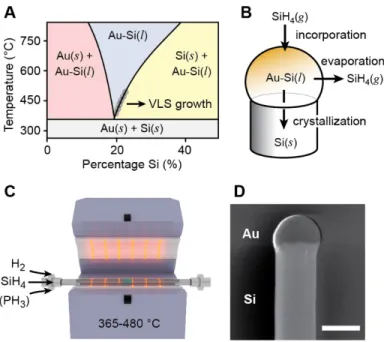
Semiconductor NWs may be synthesized by a variety of techniques, such as vapor-liquid-solid (VLS) growth, vapor-vapor-liquid-solid-vapor-liquid-solid (VSS) growth, or solution-liquid-vapor-liquid-solid (SLS) growth. These synthetic techniques typically utilize a metallic nanoparticle to facilitate growth along a particular crystallographic orientation of the semiconductor material, which produces wire-like structures with high aspect ratios. As such, metal-semiconductor binary phase diagrams, such as the Au-Si phase diagram depicted in Fig. 1.1, play an important role in choosing proper synthetic conditions. The Au-Si phase diagram was chosen because all NWs discussed in this thesis are Si with an Au catalyst. Also, the Au-Si system is a model system for semiconductor NW growth. The concepts learned from studying this system can be applied to other semiconductor-metal combinations to produce NWs of other semiconductor materials, such as Ge or GaAs.
Figure 1.1 Au-Si Binary Phase Diagram
1.2.1 Vapor-Liquid-Solid Mechanism
has become the most popular technique because it enables precise control of important nanowire properties, such as diameter14 or composition.15 Au-catalyzed VLS growth of Si NWs begins with a solid Au nanoparticle of a specified diameter. The Au nanoparticle is heated above the eutectic temperature (363 °C) in an inert atmosphere. To initiate VLS growth, a vapor phase Si precursor (e.g. SiH4, Si2H6, or SiCl4) is introduced. The Au nanoparticle catalyzes the decomposition of the
Si precursor and a AuSi liquid alloy forms. With the continued supply of the Si precursor, the Si concentration in the liquid alloy catalyst particle increases, eventually supersaturating the alloy with Si (i.e. the system is forced to the right of the liquidus line in Fig. 1.1). At this point, solid Si crystallizes from the liquid catalyst and the NW begins to grow. The duration of Si precursor flow controls the NW length, while the Au catalyst size determines the NW diameter.
1.2.2 Vapor-Solid-Solid Mechanism
While the VLS mechanism is the most widely used synthetic technique to produce NWs, it comes with a few drawbacks. Most notably, it is unable to provide atomic scale control over the NW composition. To achieve this level of control, one cannot use a liquid catalyst because it acts as a reservoir of material when changing the NW composition (see section 1.5 for a more detailed discussion of this effect).16 The VSS growth mechanism, which uses a solid catalyst instead of a
conditions. The ability to repeatedly switch between VLS and VSS mechanisms allows one utilize the advantages of each while avoiding their respective drawbacks.
1.3 Understanding Nanowire Growth Mechanisms
To produce NWs of sufficient quality for technological applications, one must precisely control the NW physical properties, such as diameter, crystallinity, uniformity, and composition. The VLS and VSS mechanisms provide the necessary synthetic control to achieve this through controlling reaction parameters such as the catalyst size, temperature, pressure, precursor flow rates, or precursor chemistry. However, this is predicated on a thorough understanding of the nuances associated with these growth mechanisms. For instance, the crystallographic direction a NW grows along depends on the temperature,19-21 pressure,22-24 catalyst composition,25-26 and NW sidewall chemistry25, 27-29 (which is controlled through precursor chemistry). A change in growth
direction, commonly referred to as kinking, is detrimental in device applications where straight NWs are needed; however, controlled kinking enables the design of more complex devices built around NWs, such as Si NW FETs that can probe individual cells.30
Much like kinking, non-catalytic deposition of semiconductor material on the NW sidewalls, often referred to as vapor-solid (VS) growth, is detrimental for some applications, but can also be leveraged to produce unique NW devices. For example, VS growth is catastrophic for the technique to control NW morphology introduced in Chapter 2, while Chapter 5 leverages controlled VS growth to produce high-efficiency NW-based photovoltaics. As the name suggests, VS growth occurs when the semiconductor precursor adds material directly to the NW sidewall, bypassing the liquid catalyst. The NW sidewall surface chemistry strongly affects the rate of VS growth.31-33 Adsorbates such as H, Cl, or CH3 can block VS growth.29, 31-34 Unintended VS growth,
properties, such as tapered sidewalls, unintentional doping, or low-resistance leakage pathways in electronic devices.
1.4 Characterizing and Modeling Nanowire Growth
To develop an understanding of NW synthetic processes one needs tools to characterize them and models to provide a framework for describing them. For NWs, techniques to quantify growth kinetics are central to understanding the underlying growth mechanisms. For example, studies centered around characterizing and interpreting NW growth kinetics have examined the rate-limiting step in the VLS mechanism,35-43 probed the importance of surface chemistry on NW growth,29, 32-33, 44-46 explored alternative catalyst materials,18 studied the role of O in NW growth,27 and provided detailed models of NW growth mechanisms.16, 43, 47-52
These studies have leveraged both in situ and ex situ techniques to measure NW growth rates. In general, in situ techniques have the advantage of ascertaining the instantaneous NW growth rate at all points along the wire. However, they require highly specialized equipment that interfaces an electron microscope with a CVD chamber. Consequently, all studies are done under UHV conditions, which do not accurately reflect synthetic conditions in standard hot-walled CVD reactors (~0.1-100 Torr). Ex situ techniques are far more common due to their practicality and are still useful for developing a deep understanding of NW growth mechanisms. For example, Chapters 3 and 4 of this thesis utilize ex situ characterization of NW growth kinetics to contribute new models for understanding the VLS and VSS growth mechanisms.
1.5 Controlling Nanowire Composition
length scales. This is largely due to the unique ability of the VLS mechanism to reliably produce structures with micron-scale dimensions but nanometer-scale control over composition across a wide variety of semiconductor materials. For example, Chapter 2 describes a technique for imparting sub-10 nm morphology to Si NWs by coupling precise control of the P concentration along the length of a NW with a selective etch.
Compositional NW heterostructures are formed by altering the supply of vapor-phase
precursors during VLS growth. In Si NWs, this has been demonstrated with dopant atoms (e.g.
NW p-n junctions53
) and a wide variety of material combinations that share a similar crystal
structure (e.g. Si/Ge54
or Si/InP55
). The ability to modulate the composition along a NW enables
the creation of unique NW devices, but the abruptness of these material transitions is central to
creating useful devices. When changing the composition of a NW, the liquid droplet can act as a
reservoir of material even after a precursor gas is removed, causing the heterojunction to be
broadened by a phenomenon termed the “reservoir effect”.17, 54, 56-62
Without taking special
precautions to mitigate this phenomenon, the broadening is comparable to the NW diameter,
which is too broad for many applications.
There are multiple strategies to mitigate the reservoir effect. For instance, the width of the
material transition is related to the amount of material in the liquid catalyst, which makes
reducing the solubility of the material in the catalyst an effective strategy. For liquid catalysts,
this has been demonstrated with AuGa alloys.63
Similarly, the VSS mechanism produces a solid
catalyst, which has minimal (<<1%) solubility for the semiconductor.17, 47
Abrupt compositional
changes in Si NWs using the VSS mechanism have been demonstrated with dopants in
Au-catalyzed NWs64 and with Ge in AuAl- and AuAg-catalyzed NWs.17-18 Alternatively, one can
shorten the transition width, opposed to limiting its solubility. For example, properly tuned VLS
growth conditions enable sub-5 nm dopant transitions in Au-catalyzed Si NWs by promoting
REFERENCES
1. Deotare, P. B.; McCutcheon, M. W.; Frank, I. W.; Khan, M.; Lončar, M., High quality factor photonic crystal nanobeam cavities. Appl. Phys. Lett. 2009, 94 (12), 121106.
2. Novotny, L.; van Hulst, N., Antennas for light. Nature Photonics 2011, 5 (2), 83-90. 3. Lieber, C. M., Nanoscale science and technology: building a big future from small things. MRS Bull. 2003, 28 (07), 486-491.
4. Yang, P.; Yan, R.; Fardy, M., Semiconductor nanowire: what's next? Nano Lett. 2010, 10 (5), 1529-36.
5. Hochbaum, A. I.; Yang, P., Semiconductor nanowires for energy conversion. Chem. Rev. 2010, 110 (1), 527-46.
6. Kempa, T. J.; Day, R. W.; Kim, S.-K.; Park, H.-G.; Lieber, C. M., Semiconductor nanowires: a platform for exploring limits and concepts for nano-enabled solar cells. Energy Environ. Sci. 2013, 6 (3), 719-733.
7. Zhang, X.; Pinion, C. W.; Christesen, J. D.; Flynn, C. J.; Celano, T. A.; Cahoon, J. F., Horizontal Silicon Nanowires with Radial p–n Junctions: A Platform for Unconventional Solar Cells. J. Phys. Chem. Lett. 2013, 4 (12), 2002-2009.
8. Qian, F.; Li, Y.; Gradečak, S.; Wang, D.; Barrelet, C. J.; Lieber, C. M., Gallium Nitride-Based Nanowire Radial Heterostructures for Nanophotonics. Nano Lett. 2004, 4 (10), 1975-1979.
9. Law, M.; Sirbuly, D. J.; Johnson, J. C.; Goldberger, J.; Saykally, R. J.; Yang, P. D., Nanoribbon waveguides for subwavelength photonics integration. Science 2004, 305 (5688), 1269-1273.
10. Cui, Y.; Wei, Q. Q.; Park, H. K.; Lieber, C. M., Nanowire nanosensors for highly sensitive and selective detection of biological and chemical species. Science 2001, 293 (5533), 1289-1292.
11. Boukai, A. I.; Bunimovich, Y.; Tahir-Kheli, J.; Yu, J. K.; Goddard, W. A., 3rd; Heath, J. R., Silicon nanowires as efficient thermoelectric materials. Nature 2008, 451 (7175), 168-71. 12. Hochbaum, A. I.; Chen, R.; Delgado, R. D.; Liang, W.; Garnett, E. C.; Najarian, M.; Majumdar, A.; Yang, P., Enhanced thermoelectric performance of rough silicon nanowires. Nature 2008, 451 (7175), 163-7.
14. Cui, Y.; Lauhon, L. J.; Gudiksen, M. S.; Wang, J. F.; Lieber, C. M., Diameter-controlled synthesis of single-crystal silicon nanowires. Applied Physics Letters 2001, 78 (15), 2214-2216. 15. Lauhon, L. J.; Gudiksen, M. S.; Lieber, C. M., Semiconductor nanowire heterostructures. Philos T Roy Soc A 2004, 362 (1819), 1247-1260.
16. Christesen, J. D.; Pinion, C. W.; Zhang, X.; McBride, J. R.; Cahoon, J. F., Encoding Abrupt and Uniform Dopant Profiles in Vapor-Liquid-Solid Nanowires by Suppressing the Reservoir Effect of the Liquid Catalyst. Acs Nano 2014, 8 (11), 11790-11798.
17. Wen, C. Y.; Reuter, M. C.; Bruley, J.; Tersoff, J.; Kodambaka, S.; Stach, E. A.; Ross, F. M., Formation of Compositionally Abrupt Axial Heterojunctions in Silicon-Germanium
Nanowires. Science 2009, 326 (5957), 1247-1250.
18. Chou, Y. C.; Wen, C. Y.; Reuter, M. C.; Su, D.; Stach, E. A.; Ross, F. M., Controlling the growth of Si/Ge nanowires and heterojunctions using silver-gold alloy catalysts. ACS Nano 2012, 6 (7), 6407-15.
19. Wagner, R. S.; Doherty, C. J., Mechanism of Branching and Kinking during Vls Crystal Growth. J Electrochem Soc 1968, 115 (1), 93-&.
20. Madras, P.; Dailey, E.; Drucker, J., Kinetically Induced Kinking of Vapor-Liquid-Solid Grown Epitaxial Si Nanowires. Nano Lett 2009, 9 (11), 3826-3830.
21. Lee, G.; Woo, Y. S.; Yang, J. E.; Lee, D.; Kim, C. J.; Jo, M. H., Directionally Integrated VLS Nanowire Growth in a Local Temperature Gradient. Angew Chem Int Edit 2009, 48 (40), 7366-7370.
22. Dailey, E.; Madras, P.; Drucker, J., Composition and growth direction control of epitaxial vapor-liquid-solid-grown SiGe nanowires. Applied Physics Letters 2010, 97 (14).
23. Lugstein, A.; Steinmair, M.; Hyun, Y. J.; Hauer, G.; Pongratz, P.; Bertagnolli, E., Pressure-induced orientation control of the growth of epitaxial silicon nanowires. Nano Lett 2008, 8 (8), 2310-2314.
24. Tian, B. Z.; Xie, P.; Kempa, T. J.; Bell, D. C.; Lieber, C. M., Single-crystalline kinked semiconductor nanowire superstructures. Nat Nanotechnol 2009, 4 (12), 824-829.
25. Kawashima, T.; Mizutani, T.; Nakagawa, T.; Torii, H.; Saitoh, T.; Komori, K.; Fujii, M., Control of surface migration of gold particles on Si nanowires. Nano Lett 2008, 8 (1), 362-368. 26. Wang, J.; Plissard, S. R.; Verheijen, M. A.; Feiner, L. F.; Cavalli, A.; Bakkers, E. P. A. M., Reversible Switching of InP Nanowire Growth Direction by Catalyst Engineering. Nano Lett 2013, 13 (8), 3802-3806.
28. Musin, I. R.; Filler, M. A., Chemical Control of Semiconductor Nanowire Kinking and Superstructure. Nano Lett 2012, 12 (7), 3363-3368.
29. Shin, N.; Filler, M. A., Controlling Silicon Nanowire Growth Direction via Surface Chemistry. Nano Lett 2012, 12 (6), 2865-2870.
30. Xu, L.; Jiang, Z.; Qing, Q.; Mai, L. Q.; Zhang, Q. J.; Lieber, C. M., Design and Synthesis of Diverse Functional Kinked Nanowire Structures for Nanoelectronic Bioprobes. Nano Lett 2013, 13 (2), 746-751.
31. Gentile, P.; Solanki, A.; Pauc, N.; Oehler, F.; Salem, B.; Rosaz, G.; Baron, T.; Den Hertog, M.; Calvo, V., Effect of HCl on the doping and shape control of silicon nanowires. Nanotechnology 2012, 23 (21).
32. Musin, I. R.; Boyuk, D. S.; Filler, M. A., Surface chemistry controlled diameter-modulated semiconductor nanowire superstructures. J Vac Sci Technol B 2013, 31 (2).
33. Musin, I. R.; Shin, N.; Filler, M. A., Diameter modulation as a route to probe the vapour-liquid-solid growth kinetics of semiconductor nanowires. Journal of Materials Chemistry C 2014, 2 (17), 3285-3291.
34. Sivaram, S. V.; Shin, N.; Chou, L. W.; Filler, M. A., Direct Observation of Transient Surface Species during Ge Nanowire Growth and Their Influence on Growth Stability. Journal of the American Chemical Society 2015, 137 (31), 9861-9869.
35. Bootsma, G. A.; Gassen, H. J., A Quantitative Study on the Growth of Silicon Whiskers from Silane and Germanium Whiskers from Germane. J. Cryst. Growth 1971, 10 (3), 223-234. 36. Givargizov, E. I., Fundamental Aspects of Vls Growth. Journal of Crystal Growth 1975, 31 (Dec), 20-30.
37. Weyher, J., Some Notes on the Growth Kinetics and Morphology of VLS Silicon Crystals Grown with Platinum and Gold as Liquid-Forming Agents. J. Cryst. Growth 1978, 43 (2), 235-244.
38. Kikkawa, J.; Ohno, Y.; Takeda, S., Growth rate of silicon nanowires. Applied Physics Letters 2005, 86 (12), 123109.
39. Kodambaka, S.; Tersoff, J.; Reuter, M. C.; Ross, F. M., Diameter-Independent Kinetics in the Vapor-Liquid-Solid Growth of Si Nanowires. Phys. Rev. Lett. 2006, 96 (9), 096105. 40. Lew, K.-K.; Redwing, J. M., Growth characteristics of silicon nanowires synthesized by vapor–liquid–solid growth in nanoporous alumina templates. Journal of Crystal Growth 2003, 254 (1-2), 14-22.
42. Dubrovskii, V.; Sibirev, N.; Cirlin, G.; Soshnikov, I.; Chen, W. H.; Larde, R.; Cadel, E.; Pareige, P.; Xu, T.; Grandidier, B.; Nys, J. P.; Stievenard, D.; Moewe, M.; Chuang, L.; Chang-Hasnain, C., Gibbs-Thomson and Diffusion-Induced Contributions to the Growth rate of Si, InP, and GaAs Nanowires. Phys. Rev. B 2009, 79 (20), 205316.
43. Dubrovskii, V. G.; Sibirev, N. V.; Cirlin, G. E., Kinetic model of the growth of nanodimensional whiskers by the vapor-liquid-crystal mechanism. Technical Physics Letters 2004, 30 (8), 682-686.
44. Musin, I. R.; Shin, N.; Filler, M. A., Diameter modulation as a route to probe the vapour– liquid–solid growth kinetics of semiconductor nanowires. Journal of Materials Chemistry C 2014.
45. Shin, N.; Filler, M. A., Controlling silicon nanowire growth direction via surface chemistry. Nano Lett 2012, 12 (6), 2865-70.
46. Kim, S.; Hill, D. J.; Pinion, C. W.; Christesen, J. D.; McBride, J. R.; Cahoon, J. F., Designing Morphology in Epitaxial Silicon Nanowires: The Role of Gold, Surface Chemistry, and Phosphorus Doping. Acs Nano 2017.
47. Wen, C. Y.; Tersoff, J.; Reuter, M. C.; Stach, E. A.; Ross, F. M., Step-Flow Kinetics in Nanowire Growth. Phys Rev Lett 2010, 105 (19).
48. Pinion, C. W.; Hill, D. J.; Christesen, J. D.; McBride, J. R.; Cahoon, J. F., Barrierless Switching between a Liquid and Superheated Solid Catalyst during Nanowire Growth. J Phys Chem Lett 2016, 7 (20), 4236-4242.
49. Pinion, C. W.; Nenon, D. P.; Christesen, J. D.; Cahoon, J. F., Identifying crystallization- and incorporation-limited regimes during vapor-liquid-solid growth of Si nanowires. ACS Nano 2014, 8 (6), 6081-8.
50. Givargizov, E. I.; Chernov, A. A., Growth-Rate of Whiskers Grown by Vapor-Liquid-Solid Mechanism, and Role of Surface-Energy. Kristallografiya 1973, 18 (1), 147-153. 51. Dubrovskii, V. G.; Sibirev, N. V.; Cirlin, G. E.; Harmand, J. C.; Ustinov, V. M.,
Theoretical analysis of the vapor-liquid-solid mechanism of nanowire growth during molecular beam epitaxy. Physical Review E 2006, 73 (2).
52. Dubrovskii, V. G.; Sibirev, N. V.; Suris, R. A.; Cirlin, G. E.; Ustinov, V. M.;
Tchernysheva, M.; Harmand, J. C., The role of surface diffusion of adatoms in the formation of nanowire crystals. Semiconductors 2006, 40 (9), 1075-1082.
55. Hocevar, M.; Immink, G.; Verheijen, M.; Akopian, N.; Zwiller, V.; Kouwenhoven, L.; Bakkers, E., Growth and optical properties of axial hybrid III-V/silicon nanowires. Nat. Commun. 2012, 3.
56. Ross, F. M., Controlling nanowire structures through real time growth studies. Rep. Prog. Phys. 2010, 73 (11).
57. Dick, K. A.; Bolinsson, J.; Borg, B. M.; Johansson, J., Controlling the Abruptness of Axial Heterojunctions in III-V Nanowires: Beyond the Reservoir Effect. Nano Lett 2012, 12 (6), 3200-3206.
58. Amit, I.; Givan, U.; Connell, J. G.; Paul, D. F.; Hammond, J. S.; Lauhon, L. J.;
Rosenwaks, Y., Spatially Resolved Correlation of Active and Total Doping Concentrations in VLS Grown Nanowires. Nano Lett 2013.
59. Hilse, M.; Ramsteiner, M.; Breuer, S.; Geelhaar, L.; Riechert, H., Incorporation of the dopants Si and Be into GaAs nanowires. Applied Physics Letters 2010, 96 (19).
60. Clark, T. E.; Nimmatoori, P.; Lew, K. K.; Pan, L.; Redwing, J. M.; Dickey, E. C.,
Diameter dependent growth rate and interfacial abruptness in vapor-liquid-solid Si/Si(1-x)Ge(x) heterostructure nanowires. Nano Lett 2008, 8 (4), 1246-1252.
61. Amato, M.; Palummo, M.; Rurali, R.; Ossicini, S., Silicon-Germanium Nanowires: Chemistry and Physics in Play, from Basic Principles to Advanced Applications. Chem. Rev. 2014, 114 (2), 1371-1412.
62. Ohlsson, B. J.; Bjork, M. T.; Persson, A. I.; Thelander, C.; Wallenberg, L. R.;
Magnusson, M. H.; Deppert, K.; Samuelson, L., Growth and characterization of GaAs and InAs nano-whiskers and InAs/GaAs heterostructures. Physica E-Low-Dimensional Systems &
Nanostructures 2002, 13 (2-4), 1126-1130.
63. Perea, D. E.; Li, N.; Dickerson, R. M.; Misra, A.; Picraux, S. T., Controlling Heterojunction Abruptness in VLS-Grown Semiconductor Nanowires via in situ Catalyst Alloying. Nano Lett 2011, 11 (8), 3117-3122.
CHAPTER 2: SYNTHETICALLY ENCODING 10-nm MORPHOLOGY IN SILICON NANOWIRES 1
2.1 Introduction
Most semiconductor technologies rely on the ability to pattern materials with nanometer-scale features using top-down lithographic tools. Over the last decade, however, bottom-up chemical methods to control the size, shape, and composition of nanoscale materials have progressed rapidly, resulting in a diverse set of well-controlled morphologies including dots, rods, ribbons, and wires.1-3 Semiconductor NWs are recognized as an especially important technological building block because the high aspect ratio can be used for longitudinal transport of electrical or optical signals.1,2 A variety of devices have been demonstrated, including sensors,4 waveguides,5 phase-change memory,6 light-emitting diodes,7 and solar cells.8-11 Nevertheless, current NW-based technology has been limited by the material’s translational symmetry and the inability to pattern arbitrary, nanometer-scale morphological features.
NWs are typically synthesized using the VLS mechanism,12 in which a metal nanoparticle catalyzes one-dimensional growth of a single-crystalline semiconductor material. Advancements in VLS-based technologies have generally involved synthesis of new materials or heterostructures.13 For instance, NW superlattices, in which the composition of a NW is modulated
along the growth axis, have been reported for Si/SiGe,14 GaAs/GaP,15 InAs/InP,16,17 Zn-doped
1 This chapter previously appeared as an article in Nano Letters. The original citation is as follows:
InP,18 CdSe/ZnSe,19 and P-doped Si.20 Modulation of NW composition often results in faceting of
the NW surface, providing some capability to control morphology during synthesis.17,18,21 In addition, NW superstructures have been reported in the form of controllably kinked NWs that break the one-dimensional shape.22,23 Nevertheless, only a handful of reports describe efforts to alter the NW geometry and encode specific morphology. For example, controlled vapor-solid over-coating on the NW surface has been used to create tapered structures24 and periodic variations in
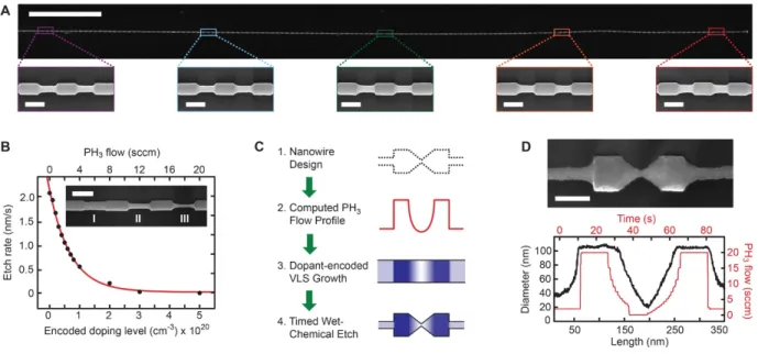
Figure 2.1: Synthesis of Si NWs with encoded morphology
(A) Schematic illustration of NW growth including rapid modulation of P dopant incorporation to form heavily-doped n-type (n) and undoped intrinsic (i) segments that are selectively etched using wet-chemical methods to form a grating. (B) SEM image of a NW grating encoded (from left to right) with sequential intrinsic segments for 200, 100, 50, 25, 10, and 5 s; scale bar, 500 nm.
2.2 Nanowire Synthesis and Etching
Si NWs were grown by a VLS mechanism in a home-built, hot-wall chemical vapor deposition (CVD) system at 420 °C using Au nanoparticles as catalysts, silane (SiH4) as the source
of Si, and hydrogen (H2) as the carrier gas (see section 2.6.1 for details). As illustrated
schematically in Fig. 2.1A, an additional flow of phosphine (PH3) was rapidly modulated during
growth20 to encode varying levels of P, an n-type substitutional dopant with high solubility in Si.
30-32 The etch rate of doped Si with aqueous KOH solution is well-known to decrease with higher
dopant concentration.33 This effect has been observed in doped Si NWs, producing changes in diameter along the axis.34,35 Here, we develop this effect as a tool to encode arbitrary,
2.3 Optimization of ENGRAVE Technique
To delineate the spatial resolution of the ENGRAVE process, we synthesized NWs with six intrinsic segments encoded along the axis for increasingly short time scales. As shown in Fig. 2.1B, wet-chemical etching of these segments yielded an abrupt and conformal reduction in the NW diameter. The largest segment, encoded for 200 s, produced a feature ~700 nm in length while the smallest segment, encoded for 5 s, produced a feature ~10 nm in length, defining the lower limit of the spatial resolution for this process. This example also demonstrates that NW growth time is directly proportional to spatial length scale. Quantitative analysis of the NW growth rate yielded a value of 213 ± 6 nm/min, which was used throughout this work to convert growth times to length scales. This rate is comparatively slow because of the low CVD temperature, 420 °C, chosen to minimize radial over-coating and doping of the NW surface, a known problem during Si NW synthesis.36,37 By minimizing the over-coating, we could encode high-fidelity nanoscale features over macroscopic length scales, as exemplified in Fig. 2.2A by the 400 nm-pitch grating encoded over 50 µm of a single NW.
dependence of the Fermi level position on the doping level, which modulates the rate of Si oxidation and dissolution at the semiconductor-solution interface.33
Figure 2.2: Characterization of NW growth, etching, and morphology
The precise calibration of the NW growth and etch rates enables rational design and synthesis of arbitrary high-resolution morphologies, as outlined schematically in Fig. 2.2C. This process involves 1) design of the morphological profile, 2) conversion of the physical profile into a dopant profile, 3) VLS growth of the dopant-encoded NW, and 4) wet-chemical etching. As an example, we used this procedure to form the bow-tie structure depicted in Fig. 2.2D. The phosphine flow profile for the bow-tie (red curve Fig. 2.2D) is complex, requiring over 25 changes in flow rate over a time scale of one minute. The diameter profile (black curve Fig. 2.2D) shows the resulting structure to be smoothly tapered with a monotonically decreasing then increasing diameter that reduces to a diameter of ~15 nm at the narrowest point. Note that the phosphine flow profile was modified to be asymmetric around the flow minimum to account for dopants retained by the Au catalyst, a phenomenon termed the reservoir effect.38
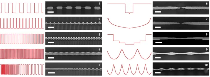
Figure 2.3: SEM images and phosphine flow profiles for the synthesis of Si NWs with complex morphology
The measured phosphine flow profile used to encode the morphology of each segment is depicted in red to the left of each SEM image; all scale bars, 200 nm. The flow rates vary from 0 to 20 sccm for each NW.
2.4 Applications of ENGRAVE
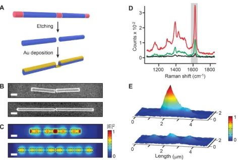
Figure 2.4: Nanogap-encoded NWs for plasmonics
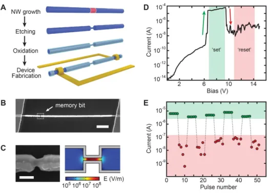
As a second application of ENGRAVE, we fabricated core/shell Si/SiO2 nanorod-encoded
devices for use as resistive switches in non-volatile memory.6,48,49 The fabrication steps are illustrated in Fig. 2.5A. First, an n-type/intrinsic/n-type NW was synthesized with a 50 nm intrinsic channel. Second, the channel was etched to a diameter of ~30 nm to produce a suspended nanorod, and third the wire was thermally oxidized to create a ~10 nm diameter Si core encased by an oxide shell. Fourth, electrical contacts were fabricated to the two n-type segments adjacent to the intrinsic channel, as shown by the SEM image in Fig. 2.5B. Device simulations50 (see Fig. 2.5C) indicate that this geometry concentrates the voltage drop and electric field within the narrow channel region, enabling a resistive switching effect as observed in a planar Si/SiO2 system.48,49 Initial
current-voltage (I-V) measurements showed an Ohmic response from the device with a resistance of 54.7 kΩ, indicating the presence of a thin Si filament encapsulated by the SiO2 shell. After an
electroforming process consisting of multiple I-V sweeps at high bias (see section 2.6.2), the device converged to the characteristic ‘switching’ I-V behavior (see Fig. 2.5D) expected from a Si/SiO2
system.48,49 The I-V curve exhibits a low voltage region that ‘sets’ the device to a low resistance state and a high voltage region that ‘resets’ the device to a high resistance state.
Figure 2.5: Nanorod-encoded NWs for non-volatile memory
(A) Schematic illustration of the sequential process used to fabricate a non-volatile memory bit. (B) SEM image of a NW device encoded with a non-volatile memory bit (dashed box) showing Ti/Pd Ohmic contacts on the far left and right; scale bar, 1 µm. (C) Left: SEM image of the encoded memory bit corresponding to the dashed white box in panel B; scale bar, 100 nm. Right: finite-element simulation of the electric field magnitude across the NW at an applied bias of +8 V plotted in a logarithmic color scale for a nanorod segment 50 nm in length and 10 nm in diameter. (D) Characteristic switching I-V curve for an ENGRAVE NW memory device. The shaded green and red regions define the ‘set’ and ‘reset’ bias ranges, respectively. (E) Resistive switching behavior over ten memory cycles. Dashed lines represent the ‘set’/’reset’ pulses between current readings, which were acquired five times at 1 V between each ‘set’ or ’reset’ pulse.
In summary, we have demonstrated a method, termed ENGRAVE, to encode high-resolution morphology along the growth axis of Si NWs. We anticipate this process will be extended to other NW materials, such as GaAs/GaP51 et al., that can be selectively etched with gas-phase or wet-chemical techniques and will represent a general route to encode new functionality in semiconductor NWs.
2.6 Detailed Methods 2.6.1 Nanowire Growth
Si NWs were grown with a home-built, hot-wall CVD system using SiH4 (Voltaix), PH3
(Voltaix; diluted to 1000 ppm in H2), and H2 (Matheson TriGas 5N semiconductor grade) gases.
The CVD system consists of a quartz tube furnace (Lindberg Blue M) with 1 inch diameter bore, fast-responding mass-flow controllers (MKS Instruments P4B), a pressure control system (MKS Instruments 250E), and vacuum system with base pressure of 1x10⁻⁴ Torr. The CVD system was computer-controlled using custom Labview software to enable rapid and reproducible modulation of the NW growth conditions and gas flow rates. Calibration runs indicated that changes in flow rate were achieved on time scales <1 s and that complete exchange of gas within the quartz tube was achieved on a time scale of ~5 s. Thus the resolution of ENGRAVE structures was primarily limited by the kinetics of the NW growth or etching process and not by the mechanics of the CVD system. For a typical NW growth run, citrate-stabilized ~100 nm Au catalysts (BBI International) were dispersed on 2 cm x 1 cm Si wafers (University Wafer; p-type Si with 600 nm thermal oxide) that had been functionalized with poly-L-lysine solution (Aldrich). These growth substrates were inserted into the center of the tube furnace, and the furnace temperature was ramped to 450 °C to nucleate NW growth for between 5 to 60 min using 2.00 sccm SiH4 and 200.0 sccm H2 at 40.0
ENGRAVE structures were encoded by introducing PH3 gas with a tightly controlled flow profile,
as discussed in the text.
2.6.2 Etching and Device Fabrication
To fabricate ENGRAVE structures, NWs were transferred from the growth substrates onto Si wafers coated with 100 nm thermal oxide and 200 nm Si nitride (Nova Electronic Materials). NWs, which were then lying flat on the substrate, were etched by immersing in concentrated buffered hydrofluoric acid (Transense BHF Improved) for 10 s, rinsing in water and isopropanol, etching in KOH solution (20.0 g KOH; 80.0 g water; 20 mL isopropanol as top surface layer) at 40 °C for variable times up to 90 s, and rinsing in water and isopropanol. To fabricate Si NWs with Noble metal structures, Si NWs were etched as described above and then placed in an electron-beam evaporator (Thermionics VE-100) for deposition of 50 nm Au at normal incidence with a rate of ~1 Å/s at a pressure <1x10⁻⁷ Torr. Thermal oxidation of NWs was performed for 3 min in a quartz tube furnace with 100 Torr O2 at 1000 °C. NW devices were fabricated by defining metal
2.6.3 Electron and Raman Microscopy
SEM imaging was performed with an FEI Helios 600 Nanolab Dual Beam system with an imaging resolution <5 nm using a typical acceleration voltage of 5 kV and imaging current of 86 pA. Raman imaging was performed with a Renishaw inVia Raman microscope using a HeNe laser source at 633 nm and 50x objective. Spectra were collected by raster scanning the sample in steps of 100 nm using an averaging time of 1.0 s. Prior to Raman image collection, the Au-coated substrates were immersed in an aqueous solution of methylene blue (Aldrich), rinsed with water, and dried with flowing N2. Three-dimensional plots of the Raman signal were generated by
summing all counts within the 1580-1650 cm-1 spectral window. 2.6.4 Finite-Element simulations
REFERENCES
1. Lieber, C. M., Semiconductor nanowires: A platform for nanoscience and nanotechnology. MRS Bulletin 2011, 36, 1052-1063.
2. Yang, P.; Yan, R.; Fardy, M., Semiconductor nanowire: what's next? Nano Lett. 2010, 10 (5), 1529-1536.
3. Choi, C. L.; Alivisatos, A. P., From artificial atoms to nanocrystal molecules: Preparation and properties of more complex nanostructures. In Annual Review of Physical Chemistry, Leone, S. R.; Cremer, P. S.; Groves, J. T.; Johnson, M. A.; Richmond, G., Eds. Annual Reviews: Palo Alto, 2010, pp 369-389.
4. Cui, Y.; Wei, Q.; Park, H.; Lieber, C. M., Nanowire nanosensors for highly sensitive and selective detection of biological and chemical species. Science. 2001, 293 (5533), 1289-1292.
5. Law, M.; Sirbuly, D. J.; Johnson, J. C.; Goldberger, J.; Saykally, R. J.; Yang, P. D., Nanoribbon waveguides for subwavelength photonics integration. Science 2004, 305 (5688), 1269-1273.
6. Lee, S.-H.; Jung, Y.; Agarwal, R., Highly scalable non-volatile and ultra-low-power phase-change nanowire memory. Nat Nano 2007, 2 (10), 626-630.
7. Qian, F.; Li, Y.; Gradečak, S.; Wang, D.; Barrelet, C. J.; Lieber, C. M., Gallium nitride-based nanowire radial heterostructures for nanophotonics. Nano Lett. 2004, 4 (10), 1975-1979.
8. Tian, B.; Kempa, T. J.; Lieber, C. M., Single nanowire photovoltaics. Chem. Soc. Rev. 2009, 38 (1), 16-24.
9. Kempa, T. J.; Day, R. W.; Kim, S.-K.; Park, H.-G.; Lieber, C. M., Semiconductor nanowires: a platform for exploring limits and concepts for nano-enabled solar cells. Energ Environ Sci 2013, 6 (3), 719-733.
10. Zhang, X.; Pinion, C. W.; Christesen, J. D.; Flynn, C. J.; Celano, T. A.; Cahoon, J. F., Horizontal silicon nanowires with radial p–n junctions: A platform for unconventional solar cells. J. Phys. Chem. Lett. 2013, 4, 2002-2009.
11. Hochbaum, A. I.; Yang, P. D., Semiconductor Nanowires for Energy Conversion. Chemical reviews 2010, 110 (1), 527-546.
12. Wagner, R. S.; Ellis, W. C., Vapor-liquid-solid mechanism of single crystal growth. Appl Phys Lett 1964, 4 (5), 89-90.
14. Wu, Y. Y.; Fan, R.; Yang, P. D., Block-by-block growth of single-crystalline Si/SiGe superlattice nanowires. Nano letters 2002, 2 (2), 83-86.
15. Gudiksen, M. S.; Lauhon, L. J.; Wang, J.; Smith, D. C.; Lieber, C. M., Growth of nanowire superlattice structures for nanoscale photonics and electronics. Nature. 2002, 415 (6872), 617-620.
16. Bjork, M. T.; Ohlsson, B. J.; Sass, T.; Persson, A. I.; Thelander, C.; Magnusson, M. H.; Deppert, K.; Wallenberg, L. R.; Samuelson, L., One-dimensional steeplechase for electrons realized. Nano letters 2002, 2 (2), 87-89.
17. Eymery, J.; Rieutord, F.; Favre-Nicolin, V.; Robach, O.; Niquet, Y. M.; Froberg, L.; Martensson, T.; Samuelson, L., Strain and shape of epitaxial InAs/InP nanowire superlattice measured by grazing incidence X-ray techniques. Nano letters 2007, 7 (9), 2596-2601.
18. Algra, R. E.; Verheijen, M. A.; Borgstrom, M. T.; Feiner, L.-F.; Immink, G.; van Enckevort, W. J. P.; Vlieg, E.; Bakkers, E. P. A. M., Twinning superlattices in indium phosphide nanowires. Nature 2008, 456 (7220), 369-372.
19. Laocharoensuk, R.; Palaniappan, K.; Smith, N. A.; Dickerson, R. M.; Werder, D. J.; Baldwin, J. K.; Hollingsworth, J. A., Flow-based solution-liquid-solid nanowire synthesis. Nat Nano 2013, 8 (9), 660-666.
20. Yang, C.; Zhong, Z.; Lieber, C. M., Encoding Electronic Properties by Synthesis of Axial Modulation-Doped Silicon Nanowires. Science 2005, 310 (5752), 1304-1307.
21. Ross, F. M.; Tersoff, J.; Reuter, M. C., Sawtooth Faceting in Silicon Nanowires. Physical Review Letters 2005, 95 (14), 146104.
22. Lilach, Y.; Zhang, J. P.; Moskovits, M.; Kolmakov, A., Encoding morphology in oxide nanostructures during their growth. Nano letters 2005, 5 (10), 2019-2022.
23. Tian, B.; Xie, P.; Kempa, T. J.; Bell, D. C.; Lieber, C. M., Single-crystalline kinked semiconductor nanowire superstructures. Nat. Nanotechnol. 2009, 4 (12), 824-829. 24. Chueh, Y. L.; Fan, Z. Y.; Takei, K.; Ko, H.; Kapadia, R.; Rathore, A. A.; Miller, N.; Yu,
K.; Wu, M.; Haller, E. E.; Javey, A., Black Ge based on crystalline/amorphous core/shell nanoneedle arrays. Nano letters 2010, 10 (2), 520-523.
25. Musin, I. R.; Boyuk, D. S.; Filler, M. A., Surface chemistry controlled
diameter-modulated semiconductor nanowire superstructures. J. Vac. Sci. Technol. B 2013, 31 (2), 020603-5.
27. Crawford, S.; Lim, S. K.; Gradečak, S., Fundamental Insights into Nanowire Diameter Modulation and the Liquid/Solid Interface. Nano letters 2013.
28. Kline, T. R.; Tian, M. L.; Wang, J. G.; Sen, A.; Chan, M. W. H.; Mallouk, T. E., Template-grown metal nanowires. Inorg. Chem. 2006, 45 (19), 7555-7565.
29. Qin, L. D.; Park, S.; Huang, L.; Mirkin, C. A., On-wire lithography. Science 2005, 309 (5731), 113-115.
30. Zheng, G. F.; Lu, W.; Jin, S.; Lieber, C. M., Synthesis and fabrication of
high-performance n-type silicon nanowire transistors. Adv. Mater. 2004, 16 (21), 1890-1893. 31. Wang, Y. F.; Lew, K. K.; Ho, T. T.; Pan, L.; Novak, S. W.; Dickey, E. C.; Redwing, J.
M.; Mayer, T. S., Use of phosphine as an n-type dopant source for vapor-liquid-solid growth of silicon nanowires. Nano letters 2005, 5 (11), 2139-2143.
32. Schmid, H.; Bjork, M. T.; Knoch, J.; Karg, S.; Riel, H.; Riess, W., Doping limits of grown in situ doped silicon nanowires using phosphine. Nano letters 2009, 9 (1), 173-177.
33. Seidel, H.; Csepregi, L.; Heuberger, A.; Baumgartel, H., Anisotropic etching of crystalline silicon in alkaline solutions. 2. Influence of dopants. Journal of the Electrochemical Society 1990, 137 (11), 3626-3632.
34. Kempa, T. J.; Tian, B.; Kim, D. R.; Hu, J.; Zheng, X.; Lieber, C. M., Single and tandem axial p-i-n nanowire photovoltaic devices. Nano Lett. 2008, 8 (10), 3456-3460.
35. Cohen-Karni, T.; Casanova, D.; Cahoon, J. F.; Qing, Q.; Bell, D. C.; Lieber, C. M., Synthetically encoded ultrashort-channel nanowire transistors for fast, pointlike cellular signal detection. Nano letters 2012, 12 (5), 2639-2644.
36. Perea, D. E.; Hemesath, E. R.; Schwalbach, E. J.; Lensch-Falk, J. L.; Voorhees, P. W.; Lauhon, L. J., Direct measurement of dopant distribution in an individual vapour-liquid-solid nanowire. Nat. Nanotechnol. 2009, 4 (5), 315-319.
37. Schmid, H.; Bjork, M. T.; Knoch, J.; Riel, H.; Riess, W.; Rice, P.; Topuria, T., Patterned epitaxial vapor-liquid-solid growth of silicon nanowires on Si(111) using silane. Journal of Applied Physics 2008, 103 (2), 024304.
38. Wen, C. Y.; Reuter, M. C.; Bruley, J.; Tersoff, J.; Kodambaka, S.; Stach, E. A.; Ross, F. M., Formation of compositionally abrupt axial heterojunctions in silicon-germanium nanowires. Science. 2009, 326 (5957), 1247-1250.
40. Lindquist, N. C.; Nagpal, P.; McPeak, K. M.; Norris, D. J.; Oh, S. H., Engineering
metallic nanostructures for plasmonics and nanophotonics. Rep. Prog. Phys. 2012, 75 (3), 036501.
41. Hochbaum, A. I.; Chen, R.; Delgado, R. D.; Liang, W.; Garnett, E. C.; Najarian, M.; Majumdar, A.; Yang, P., Enhanced thermoelectric performance of rough silicon nanowires. Nature. 2008, 451 (7175), 163-167.
42. Zianni, X., Diameter-modulated nanowires as candidates for high thermoelectric energy conversion efficiency. Appl Phys Lett 2010, 97 (23), 233106.
43. Willets, K. A.; Van Duyne, R. P., Localized surface plasmon resonance spectroscopy and sensing. In Annu. Rev. Phys. Chem., Annual Reviews: Palo Alto, 2007, pp 267-297. 44. Schuller, J. A.; Barnard, E. S.; Cai, W.; Jun, Y. C.; White, J. S.; Brongersma, M. L.,
Plasmonics for extreme light concentration and manipulation. Nature Materials 2010, 9 (3), 193-204.
45. Barnard, E. S.; White, J. S.; Chandran, A.; Brongersma, M. L., Spectral properties of plasmonic resonator antennas. Optics Express 2008, 16 (21), 16529-16537.
46. Pedano, M. L.; Li, S. Z.; Schatz, G. C.; Mirkin, C. A., Periodic electric field enhancement along gold rods with nanogaps. Angewandte Chemie-International Edition 2010, 49 (1), 78-82.
47. Li, S. Z.; Pedano, M. L.; Chang, S. H.; Mirkin, C. A.; Schatz, G. C., Gap Structure Effects on Surface-Enhanced Raman Scattering Intensities for Gold Gapped Rods. Nano letters 2010, 10 (5), 1722-1727.
48. Yao, J.; Sun, Z.; Zhong, L.; Natelson, D.; Tour, J. M., Resistive switches and memories from silicon oxide. Nano letters 2010, 10 (10), 4105-4110.
49. Yao, J.; Zhong, L.; Natelson, D.; Tour, J. M., In situ imaging of the conducting filament in a silicon oxide resistive switch. Scientific Reports 2012, 2.
50. Christesen, J. D.; Zhang, X.; Pinion, C. W.; Celano, T. A.; Flynn, C. J.; Cahoon, J. F., Design principles for photovoltaic devices based on Si nanowires with axial or radial p–n junctions. Nano letters 2012, 12 (11), 6024-6029.
51. Kallesoe, C.; Molhave, K.; Larsen, K. F.; Engstrom, D.; Hansen, T. M.; Boggild, P.; Martensson, T.; Borgstrom, M.; Samuelson, L., Integration, gap formation, and
CHAPTER 3: IDENTIFYING CRYSTALLIZATION AND INCORPORATION LIMITED REGIMES DURING VAPOR-LIQUID-SOLID GROWTH OF SI
NANOWIRES1 3.1 Introduction
Semiconductor NWs have been widely explored as a fundamental building block of nanoscale devices1-2 that can be used for optoelectronics,3-4 photovoltaics,5-8 and electronics.9-11 NWs are typically synthesized by the VLS mechanism, which was originally proposed by Wagner and Ellis fifty years ago.12-14 In the VLS process, vapor-phase semiconductor material is supplied to a metal catalyst, which forms a liquid alloy droplet because of a low eutectic temperature between the metal and semiconductor. For example, the eutectic temperature for Au and Si is ~363 °C (see the binary phase diagram in Figure 3.1A), enabling the formation of liquid droplets composed of ~20% Si above this temperature. During VLS growth, supersaturation of the liquid catalyst induces crystallization of the semiconductor material and elongation of the NW at the liquid-solid interface. These general aspects of the VLS mechanism are well known; however, the microscopic kinetic and physical processes that determine the overall NW growth rate remain poorly understood and debated in the literature.
The VLS process has been demonstrated with a range of semiconductor materials including group IV Si,12-13 Ge,15 and group III-V GaAs,16 GaN,17 InP,18 etc materials as well as a range of metal catalysts including Au,12-13 Ag,19 Pt,20-21 etc. For NW-based technologies, synthetic control
1
of the VLS process has been used to control NW size,22-23 composition,16, 24-25 and morphology11, 26-28 in order to encode specific functionality in the NW material. For group IV NWs, low-pressure
CVD with Au catalysts is often used for VLS growth in conjunction with hydride precursor gases such as silane (SiH4), disilane (Si2H6), germane (GeH4), and digermane (Ge2H6). The relatively
Figure 3.1: VLS growth of Si NWs by CVD
(A) Binary Au-Si phase diagram showing regions of solid Au, liquid Au-Si alloy, and solid Si as a function of weight percent Si. The approximate regions of the diagram accessed during the VLS growth are depicted by gray circles. (B) Illustration of the three key processes—incorporation, evaporation, and crystallization—that are used to model Si NW growth by the VLS mechanism. (C) Schematic of the hot-wall, low-pressure CVD system used for synthesis of Si NWs at temperatures of 365-480 °C. (D) SEM image of a Si NW grown using an Au catalyst ~150 nm in diameter; scale bar, 150 nm.
reaction, or associative desorption of silane gas from the Au-Si liquid surface. Finally, the crystallization process describes the nucleation of solid Si crystal planes at the liquid-solid interface, which irreversibly elongates the NW. We neglect diffusion in the Au-Si liquid catalyst because it is too rapid to be a rate-limiting step in small diameter NWs20, 30 and also neglect diffusion of adsorbed Si on the substrate or NW surface, which has been shown to be of minimal importance for Si NW growth.31 With a few exceptions,32-33 reports on the kinetics of Si NW VLS
growth generally do not include a Si evaporation or desorption process in the analysis. However, considering the principle of microscopic reversibility there is no a priori rational to exclude this reaction.
The rate-limiting step for NW growth has been debated because experimental and theoretical reports have produced conflicting results.15, 20-21, 30-31, 34-37 For instance, Bootsma and
Gassen observed a growth rate proportional to the partial pressure of silane and thus proposed an incorporation-limited mechanism.15 More recently, Lew and Redwing reported similar results, also concluding that incorporation was the rate-limiting step.30 In contradiction, Givargizov proposed a crystallization-limited mechanism because wires growing along different crystallographic directions exhibited different growth rates.20
They concluded that VLS growth proceeds by an incorporation-limited mechanism. In addition, several recent theoretical studies have shown that the NW growth process involves coupled processes and cannot necessarily be reduced to a single rate-limiting step.33, 35
3.2 Experimental Design
To help resolve the long-standing ambiguities about the VLS growth process, we performed precise experimental measurements on the growth rate of Au catalyzed Si NWs over a range of temperatures (365-480 °C), diameters (30-200 nm), and pressures (0.1-1.6 Torr SiH4).
NWs were synthesized in a hot-wall, quartz-tube CVD reactor (see schematic in Fig. 3.1C) using silane as the Si precursor, phosphine (PH3) for n-type doping with phosphorus, and hydrogen (H2)
as the carrier gas (see section 3.7.1 details of NW growth). The NW diameter was controlled by the size of the Au catalysts deposited on growth substrates. The CVD apparatus and growth conditions used for our experiments are similar to those used widely within the NW community for group IV materials.22, 39-40 All synthetic conditions used in this study produce high-quality, single-crystalline NWs, as exemplified by the scanning electron microscopy (SEM) image in Fig. 3.1D.
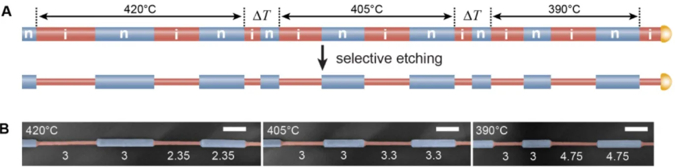
As shown in Fig. 3.2, growth rate data was generated using a modification of our recently reported method, ENGRAVE (Encoded Nanowire GRowth and Appearance using VLS and Etching),11 to sequentially encode n-type and intrinsic sections in the NWs at various temperatures and SiH4 partial pressures. Selective wet-chemical etching of the intrinsic sections (see Fig. 3.2A)
significant difference in the growth rate of n-type and intrinsic sections was observed. This method has previously been used to measure NW growth rates in both VLS11 and VSS41 mechanisms.
Figure 3.2: Determination of Si NW VLS growth rates using dopant modulation
(A) Upper: Schematic illustration of alternating n-type (n) and intrinsic (i) segments encoded sequentially during VLS NW growth at temperatures of 420, 405, and 390 °C. Sections denoted DT are not drawn to scale and correspond to regions over which the temperature was lowered at a
rate of 1 °C/min. Lower: Illustration of the NW morphology that results from etching in aqueous KOH solution, which selectively removes intrinsic sections (red) of the NW. (B) False-colored SEM images of a Si NW ~80 nm in diameter with sequential segments encoded at 420 (left), 405 (middle), and 390 °C (right). Growth times in minutes are denoted beneath each segment, and all segments were grown at a SiH4 partial pressure of 0.4 Torr and total pressure of 40 Torr; scale
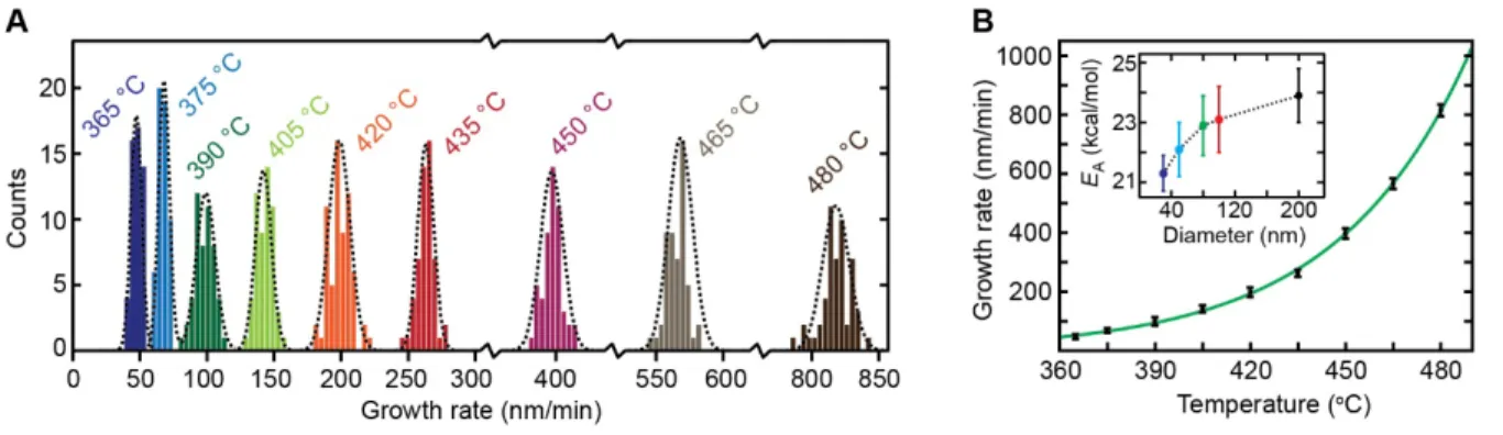
Figure 3.3: Temperature-dependent Si NW VLS growth rates
(A) Histogram of measured VLS growth rates acquired at temperatures ranging from 365 to 480 °C for NWs 80 nm in diameter at an SiH4 partial pressure of 0.4 Torr. Dashed lines represent a fit
of the data at each temperature to a Gaussian distribution. (B) Plot of growth rate vs. temperature for the data contained in panel A; error bars reflect two standard deviations (2s). The solid green line represents a fit to the Arrhenius expression. Inset: activation energy as a function of NW diameter, as determined by fits to growth rate data for NWs 30 to 200 nm in diameter.
3.3 Results
Growth rate data collected at one diameter (80 nm) and one partial pressure (0.4 Torr SiH4)
consistent with the enhanced catalytic activity observed with small-diameter Noble metal nanoparticles.44-45
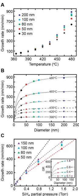
Growth rate data for diameters of 30-200 nm at a SiH4 partial pressure of 0.4 Torr are
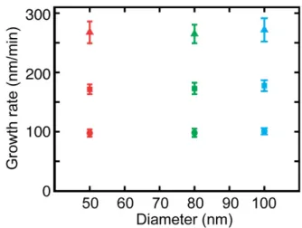
displayed as a function of temperature in Fig. 3.4A. For temperatures of 390 °C and below, we observed no statistically significant differences in the growth rates for NWs of different diameter. However, for temperatures of 435 °C and above, we observed definitively faster growth rates for larger diameter NWs. Growth rate data is plotted as a function of NW diameter in Fig. 3.4B. Low temperatures show no dependence on diameter whereas higher temperatures show a non-linear dependence, exhibiting growth rates that asymptotically increase with increasing diameter.
As shown in Fig. 3.4C, we also examined the effect of SiH4 partial pressure on the Si NW
growth rate. The pressure-dependent growth rates are not linear over the full range of synthetic conditions examined—an observation in disagreement with previous studies that reported a purely linear dependence.30-31 For the 420 °C data at low partial pressures (<0.2 Torr), the growth rate is diameter independent but at higher partial pressures (>0.2 torr) becomes diameter dependent (see inset in Fig. 3.4C). However, at 390 °C the growth rate is diameter-independent for all SiH4 partial
Figure 3.4: Diameter-dependent Si NW VLS growth rates
(A) Diameter-dependent growth rates as a function of temperature for Si NWs with diameters of 30 (black), 50 (red), 80 (green), 100 (blue), and 200 nm (indigo) at a SiH4 partial pressure of 0.4
Dashed lines represent linear fits to the data. For partial pressures <0.3 Torr, all diameters were fit simultaneously (dashed black line). For partial pressures >0.3 Torr, the 150 nm (dashed purple) and 50 nm (dashed red) data were fit separately. Inset: NW growth rate (GR; nm/min) at 420 °C as a function of diameter for SiH4 partial pressures ranging from 0.1-1.6 Torr. Dashed gray lines
represent fits to equation 9. For all panels A-C, error bars are comparable in size to the marker symbols and omitted for clarity.
Figure 3.5: Si NW growth rates at 390 oC for various partial pressures.
Diameter-independent growth kinetics at 390 oC for partial pressures of 0.4 Torr (circles), 0.8 Torr (squares), and 1.6 Torr (triangles). Plot marker color indicates NW diameter. Error bars are one standard deviation.
3.4 Kinetic Modeling
in this analysis is depicted in Fig. 3.6.
We consider a mechanism in which the incorporation step is reversible:
SiH4 𝑔 𝑘( ⇌ 𝑘*
Si(𝑙) + 4H-, (eq. 3.1)
and the crystallization step is irreversible:
Si(𝑙) 01 Si(𝑠), (eq. 3.2) where H- represents surface adsorbed hydrogen, ki the incorporation rate constant (units of s-1), ke
the evaporation rate constant (units of nm·s-1), and kc the crystallization rate constant (units of
nm·s-1). The irreversible reaction in equation 2 implicitly assumes that the supersaturation of the Au-Si droplet and the liquid-solid chemical potential, µLS, are sufficiently high to irreversibly drive
the crystallization process under all synthetic conditions. A full analysis of equations 1 and 2 under steady-state conditions, which includes the effects of surface-confined reactions at the liquid-vapor and liquid-solid interfaces (which introduces units of length to ke and kc), yields a NW growth rate,
G, of (see section 3.8 for a full derivation):
𝐺 = 01 05
06701 8 Ω 𝜌;(<*; 𝐾>/@ 𝑃 , (eq. 3.3)
where W is the volume per atom for Si, Ka/d is the silane adsorption/desorption equilibrium constant
(units of inverse pressure), rsites is the density of surface sites available for SiH4 adsorption, and P
is the partial pressure of SiH4 in the reactor. Note the quantity Ka/d·P equals the fractional
saturation, q, of SiH4 adsorption sites and would be expected to saturate (i.e. q = 1) at sufficiently
Figure 3.6: The kinetics and energetics of VLS NW growth.
Energy landscape for the VLS mechanism, depicting the barriers and rate constants associated with incorporation, evaporation, and crystallization processes that govern the kinetics leading from gaseous SiH4 to liquid AuSi to solid diamond-cubic Si.
Each rate constant in equation 3 can potentially have dependencies on temperature and diameter. In this analysis, however, we assume ki is simply described by the Arrhenius expression,
yielding the activation energies, EA, depicted in the inset of Fig. 3.3B. Although kc may have a
similar Arrhenius-type dependence on temperature that depends on the mechanism of crystallization,33 we assume that the barrier to crystallization is substantially lower than the incorporation barrier46 and thus neglect this temperature dependence for the temperature range examined in this study and treat kc as a constant value.
The Gibbs-Thomson effect, which changes the chemical potential of Si within the catalyst droplet, appears through the dependence of ke on NW diameter. The chemical potential difference
between Si in the vapor and liquid phases, µVL, is given by:33
where kB is the Boltzmann constant, T is the temperature, Po is the vapor pressure of Si in the solid
NW, CSi(l) is the concentration of Si in the supersaturated liquid droplet, Co is the equilibrium
concentration of Si in the liquid droplet, gVL is the vapor-liquid surface tension of the droplet, and
d is the diameter of the NW. The final term in equation 3.4, which scales as d-1, accounts for the decrease of µVL as a result of the curved liquid surface, which is commonly referred to as the
Gibbs-Thomson effect. As indicated by the plot in Fig. 3.6, the energetic barrier for the evaporation process is the summation of EA and µVL, yielding an Arrhenius-type expression for ke of:33
𝑘* = 𝐴 exp W XY0[7ZQR , (eq. 3.5)
where A is a pre-factor with units of nm·s-1. Substituting equation 3.4 into equation 3.5 and simplifying to first order yields:
𝑘* = 𝐴 exp WX0[Y IIJ LSi ML
J exp
N O PQR
@ 0[ ≈ 𝐴 exp
WXY 0[
IJ I
LSi M
LJ 1 +
N O PQR
@ 0[ . (eq 3.6)
Therefore, ke includes a d-1 dependence as a result of the Gibbs-Thomson effect. Note that we
assume pseudo first-order kinetics with the respect the adsorbed hydrogen concentration (i.e. we assume saturated H- coverage); thus, the pre-factor in equation 6 includes a term proportional to the hydrogen coverage (see section 3.8).
Based on this analysis, two limits of equation 3.3 can be examined. First, for kc > 2ke, the
growth rate becomes:
𝐺 ≈ 2 𝑘( Ω 𝜌;(<*; 𝐾>/@𝑃 , (eq 3.7)
and a diameter dependence is not expected as ke does not appear in the expression. This limit can
be considered an incorporation-limited regime because only ki appears in the expression. Second,
for the limit kc < 2ke , the growth rate becomes:
𝐺 ≈ 05 01Ω 𝐾
where Keq = ki·ke-1 (units of nm-1) is the equilibrium constant for incorporation/evaporation, and,
as a result, the growth rate is dependent on diameter and scales as (1+4WgVL/dkBT)-1. This limit can
be considered a crystallization-limited regime because the slower rate of crystallization relative to incorporation/evaporation induces an equilibrium between incorporation/evaporation; consequently, the growth rate scales as Keq·kc.
3.5 Analysis and Discussion
The kinetic analysis presented above yields a diameter-independent, incorporation-limited regime (equation 3.7) and a diameter-dependent, crystallization-limited regime (equation 3.8). The key mechanistic aspects of each regime are illustrated in Fig. 3.7A and 3.7B, respectively. By classifying our experimental data into these two regimes using the measured diameter dependence, we can generate the ‘phase’ diagram depicted in Fig. 3.7C, in which the incorporation-limited regime (red region) is observed at low temperatures and SiH4 partial pressures and the
Figure 3.7. Identification of crystallization-limited and incorporation-limited regimes during VLS NW growth.
(A) Illustration of the key kinetic processes for the incorporation-limited (diameter-independent) regime, which is dominated by the rate of Si incorporation from the gas phase. (B) Illustration of the key kinetic processes for the crystallization-limited (diameter-dependent) regime, which includes rapid gas-liquid equilibration and slower Si crystallization. (C) ‘Phase’ diagram depicting regions of temperature and silane partial pressure in which VLS growth is crystallization limited (shaded green), incorporation limited (shaded red), or intermediate (shaded blue). Red squares denote synthetic conditions with a independent growth rate, green circles a diameter-dependent growth rate, and blue diamonds the transition between diameter-indiameter-dependent and diameter-dependent regimes.