AUT J. Model. Simul., 50(2) (2018) 195-202 DOI: 10.22060/miscj.2018.13414.5072
Non-linear modeling, analysis, design and simulation of a solid state power amplifier
based on GaN technology for Ku band microwave application
V. Ezzati, A. Abdipour*
Department of Electrical Engineering, Amir Kabir University of Technology, Tehran, Iran
ABSTRACT: In this paper, a non-linear approach for design and analysis of solid-state power amplifiers is presented and used for AlGaN-GaN high electron-mobility transistor (HEMTs) on SiC substrate for Ku band(12.4 - 13.6 GHz) applications. With combining the output power of 8 transistors, maximum output power of 46.3 dBm (42.6 W), PAE of 43% and linear gain of 22.9 dB were achieved and good agreement has been obtained between the simulation and analysis results.
Review History:
Received: 12 September 2017 Revised: 28 April 2018 Accepted: 17 June 2018 Available Online: 27 June 2018
Keywords:
Non-linear GaN modeling power amplifier Ku band harmonic balance
1- introduction
The use of solid-state power amplifiers (SSPAs) in many radio communication systems, such as Ku band satellite communication systems, mobile cellular phone systems, etc., has significantly increased in recent years. The higher reliability of SSPAs, smaller size, and enhanced performance have resulted in an increased popularity over its traveling wave tube amplifier (TWTA) counterparts. AlGaN/GaN HEMTs have attracted much commercial interest due to the inherent advantages of their high voltage and high power density. Up to 8.1 W/mm pulsed power has been demonstrated from a 3.6-mm gate periphery device at 8 GHz [1]. 7.7 W/ mm pulsed power has also been demonstrated at 35 GHz from standard 4 × 65-μm T-gated AlGaN/GaN HEMT [2]. Two kinds of high-efficiency power amplifiers (PAs) at X (30W and 60% PAE) and Ku bands (33% PAE, 100W) utilizing 0.15 μm GaN HEMT technology are presented at [3]. 16APSK data transmission has been done for Ku band satellite broadcastings with a 100 W class SSPA with very high linearity [4].
However, for high-power operation with a large gate periphery HEMT in the Ku band and other higher frequencies, many difficulties appear. For example, with the increase of device gate periphery, the device’s impedance decreases steadily in proportion to the total gate width, which makes the external matching network design very difficult. As the chip’s width has the same order as the micro-strips in the matching circuits, it becomes difficult to feed a microwave signal uniformly to such a large transistor [5]. The parasitic effects of the connection wire and the encapsulation shell are also significant at high frequencies. In addition, the self-heating effect and the defect trapping effect in the large gate periphery devices will both be more profound [6], [7] . These problems
have prevented the easy development of large gate periphery HEMTs for high power operation with external matching circuits at high microwave frequencies. In this paper, a power amplifier with maximum output power of 46.3 dBm (42.6 W), PAE of 43% and linear gain of 22.9 dB is designed and simulated with harmonic balance analysis and a new fast algorithm instead of source pulling and load pulling. With presented design approach, power amplifiers are designed over frequency bandwidth and different input powers, which was over a single input power and single frequency in source pull and load pull algorithm. Designing for different input powers makes it possible for using in amplitude varying modulations.
In section 2, a parametric model of a GaN HEMT transistor is used for harmonic balance. Implemented harmonic balance is tested for some known scenarios and results verify parametric model, extracted parameters of model, and implemented harmonic balance algorithm. In section 3, a new design scheme is presented and a single transistor amplifier designed. Output power of 8 single transistor amplifier is combined to achieve desired output power.
2- GaN HEMT transistor
GaN HEMT transistors have higher break-down voltage, current density and electron mobility with respect to other combinations; thus, electrical current and output powers are increased [8]. Thermal resistivity is low and maximum tolerable temperature is high in GaN. This makes cooling system easier and cheaper. Maximum operating frequency in GaN transistor is high, and this makes GaN transistors suitable for generating power in microwave and mm-wave bands. These benefits are measured with some figure of merits, namely Johnson’s and Baliga’s figure of merits. As shown in [8], GaN HEMT is best choice.
2- 1- Transistor model
In this paper, a temperature-dependent large-signal model for AlGaN-GaN high electron-mobility transistors (HEMTs) is chosen [9]. This model includes thermal, RF dispersion and bias-dependent capacitance model elements, which is suitable for harmonic-balance simulator. Large-signal model topology is shown in Fig. 1. The thermal model has a current source Ith, a resistance Rth (
°
C W
/
), and a capacitance Cth. With these elements at a particular bias point, the device channel temperature T can be determined.The drain current model (Ids in Fig. 1) is based on Curtice cubic model with temperature-dependent coefficients and internal time delay of FET [9 , 10]. The current source Ith in Fig. 1 is numerically equal to the instantaneous power dissipated in FET, and the RthCth (=
τ
th) product is the thermal time constant. Package temperature T
can be determined by [9]:(1)
0
,
th ds dsT R V I
=
+
T
Where
T
0 is ambient temperature and channel temperatureT
is determined by [9]:(2)
1/1 0
0
(
)
[
]
b.
b
T b T T
T
T
−
−
−
=
With a model parameter0< <b 1.
The non-linear behavior of the bias-dependent gate-source capacitance is modeled using [11],
(3)
1 2
1
1 0 1 2 0
1 tanh[ ( )]
1
( , , ) ( )( )( ).
1 1 tanh[ ( )]
c c in fcg
v out
gs in out gs
v ds c c gs fcg
f f V v
c V
C V V T C T
c V f f V v
+ +
+ =
+ + +
Where linearized temperature-dependent capacitance between gate and source is C Tgs( )=Cgs+cgsT∆T with
0
T T T
∆ = − , the difference between the device channel and room temperature, and cgsT is the temperature coefficient, Vds0 and Vgs0 are the bias voltages used for Cgs extraction at room temperatures, and fc1, fc2, cv1, and vfcg are fitting parameters. For gate-drain capacitance, we use the following equation,
(4) 2
2 3 4
2
2 0 3 4 0
1 1 tanh( )
( , , ) ( )( )( ),
1 v in 1 c tanh( c out)
gd in out gd
v gs c c ds
c V f f V C V V T C T
c V f f V
+ −
=
+ −
with C Tgd( )=Cgd +cgdT∆T where cgdT is the temperature coefficient, and fc3, fc4, and cv2 are fitting parameters.
2- 2- Transistor model parameter extraction
The device epi-layer, fabrication, and RF testing results for AlGaN-GaN HEMTs used in this study have been previously introduced in [9], [12]. Two devices having different peripheries with a manifold gate finger arrangement were characterized, a 0.25 mm(2 125× µm) and a 1.5 mm
(12 125× µm) device, both of which had a 0.35-
µ
m gate length, a 3.0-µ
m gatedrain spacing, and a 1.0-µ
m gate-source spacing. The 1.5-mm device had substrate via-holes on the sources. The surface of the device was passivated by Si3N4. These devices had a maximum of approximately 600-mA/mm dc drain current and its pinchoff voltage was -4 V. Pulsed I-V measurements were performed in [9]. Parasitic elements in Fig. 1 were determined by using a frequency-dependent fit [13] with measured S-parameters at cold-FET conditions. The small-signal intrinsic parameters were extracted using analytical equations for the Y-parameters for an intrinsic linear device model after de-embedding the parasitic elements [9]. The bias-dependent capacitance model fitting parameters were extracted using a least mean square error fit to the S-parameter data measured at 80 bias points at various temperatures. For the extraction of the temperature-dependent coefficients Ai(T), the dc IV measured at elevated ambient temperatures, and the sets of Ai extracted using a least mean square error fit to the measured IV. The drain current parameters, i.e.λ
,β
, andγ
, were extracted by an optimized fit to the measured IV [9].2- 3- Harmonic balance analysis
For non-linear applications as power amplifier and mixer design, non-linear analysis and simulation is essential. Harmonic balance is a powerful tool in time-frequency domain. For this analysis, two constraints must be satisfied. First, device dimensions must be small relative to shortest wave length. Second, circuit must be in steady state.
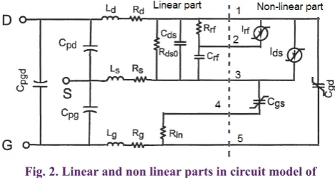
For harmonic balance analysis, first step is dividing circuit model to linear and non-linear part. In Fig. 2, this division is shown. Four non-linear elements are in non-linear part and five ports are assigned to them. Temperature circuit model is not shown in Fig. 2. After a HB analysis and calculating drain current, new temperature is calculated and iteratively they would converge. So, in each HB analysis, temperature is constant and will not change.
Linear part is represented by a 7-port network. A 7-port Y-parameter is calculated for this network at required frequencies, using Agilent ADS [2009].
Non-linear current is calculated using equations introduced in [9]. Non-linear capacitances are calculated using (3) and (4), Fig. 1. Large-signal equivalent circuit with additional RF
current source and output conductance branches are used to account for dc-RF dispersion.
and transformed to current after calculating the charge (5)
( )
( ( ))
( )
Q t
=
C V t
×
V t
and a with a differentiation, currents of capacitance are:
(6)
( )
( )
.
c
Q t
I t
t
∂
=
∂
This is easier in frequency domain as shown below: (7)
0
[ ]
[ ].
c
I k
=
jk Q k
ω
After calculating currents of current sources Ids in time domain, they are transformed to frequency domain and represented by Fourier series. Therefore, five-element current matrix of non-linear part at k’th harmonic is
(8) 0 0 0 0 [ ] [ ] [ ] [ ] [ ] [ ] [ ] [ ] [ ]
rf ds cgd
rf
ds cgs
nlp
cgs
cgd
I k I k jk Q k
I k
I k jk Q k
I k
jk Q k
jk Q k
ω ω ω ω + + − − + = − −
2- 3- 1- Solving HB equation
HB equation is a KCL at linear and non-linear junctions. So it is
(9)
I +I =0
nlp lpon any time if it is in time domain, or at any harmonic, if it is expressed in frequency domain. Non-linear currents can be calculated using (8) for a set of junction voltages. Linear currents can be calculated using Y-parameters, junction voltages and input voltages by
(10)
1 1
2 2
3 3
6 4 7 7 4
7 5 5
6 6 7 7 [ ] [ ] [ ] [ ] [ ] [ ] [ ] [ ] [ ] [ ] [ ] [ ] [ ] [ ] [ ] [ ] [ ] [ ] [ ] l l lp l l l l
I k V k
I k V k
I k I k V k
I k I k I k Y k V k
I k I k V k
I k V k
I k V k
× = = = ×
In the above relation, Il includes all linear currents, Ilp includes junction linear part currents, I6 and I7 are drain and gate (output and input) currents, respectively. Y7
×
7 is linear Y-parameters and Vi matrix represents voltages of all ports. For a given voltage, junction port currents can be written by(11)
1,6 1,7 1,1 1,5 1
6 7
5,6 5,7 5,1 5,5 5
[ ] [ ] [ ] [ ] [ ] [ ] [ ] [ ] ... [ ] [ ] [ ] ... [ ] [ ] lp
Y k Y k V k Y k Y k V k
I k V k
Y k Y k Y k Y k V k
= +
The first term is dependent on input voltage and is constant for DC term, because V6[0] and V7[0] are bias inputs and V7[1] is amplifier a constant input. Other harmonics of these two are zero. This constant matrix can be named Is[k] and (11) can be rewritten by
(12)
5 5
[ ]
[ ]
[ ]
[ ]
lp s
I k
=
I k Y
+
×k V k
×
in which V [k] includes junction port voltages at kth harmonics. Linear junction currents can be calculated using (12). Both linear and non-linear parts of current matrices are dependent on junction ports voltages. Goal of a HB analysis is to find
a suitable junction port voltages matrix, that satisfies HB equation on (9). For solving this equation, optimization can be used. Newton-Raphson can also be used, but Jacobean matrix would be complicated because of complex non-linear modeling and numerous non-non-linear elements. Another method is separating method, which is done here. In this method, a guess of voltage matrix is made, then non-linear currents (Inlp[k]) are calculated. The linear part’s currents (Ilp[k]) are calculated using equation (9), and a better voltage approximation is made with rearranged equation (12)
(13)
1 1
5 5
[ ]
[ ]
( [ ]
lp s[ ])
V k Y
k
−I k
I k
×=
×
−
This can be done until voltages matrix is converged to a stable value (VN[k]), then the analysis is finished and all voltages and currents are known.
For designing a power amplifier, a lot of bias points and matching impedances should be analysed. Changing matching impedance means changing Y-parameters matrices. In order to accelerate analysis, contribution of load and source impedances on Y-parameters are calculated and added to the equation (12) as it follows,
(14)
5 5 5 5
[ ] [ ] [ ] ( [ ] [ ]) [ ]
lp s s
I k I k I k′ Y k Y ′ k V k
× ×
= − + − ×
s
I′ and
5 5 Y ′
× are dependent on bias voltages, source, and load impedances at each harmonic. For an analysis, after selecting bias point, source, and load impedances, correcting values for
Is and Y5 5× should be calculated, and equation (14) is used instead of (12).
2- 3- 2- Verification of model and HB analysis with simulation and measurement
This harmonic balance algorithm is applied to some known problems, and results are compared to other simulators and measured data. All measured data are derived from [9]. DC operation results at some temperatures for 0.25 mm peripheries at Vgs from 0 to -3 V are shown in Fig. 3. Solid lines are harmonic balance analysis, dots are Agilent ADS harmonic balance result and dashed lines are measured data. Measurment process was performed in pulsed mode for restraining temperature at a constant value.
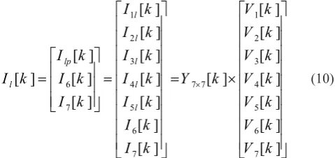
Small signal results for 1 to 26.5 GHz at 27◦ with Vds = 15V and Vgs = -2V are shown in Fig. 4. In this figure, the solid lines are harmonic balance analysis, the dashed lines are Agilent ADS simulation and the dots indicates the measured data.
Large signal results from analysis and measurement for 1.5 mm periphery AlGaN-GaN with 50-ohm load and source impedances at 27◦ are shown in Fig. 5. In this scenario, Vds = 20V , Vgs = -1.7V and input frequency was 8 GHz, which was not in Ku band, but measured data from [9] was at 8 GHz. The solid line and the dashed line are output power and gain, respectively, from analysis, and the dots represent the measured gain and the output power.
3- Non-linear GaN power amplifier design
The above results show similarity among simulation, analysis and measurement. With this model, a 40 W power amplifier at Ku band is designed. Design procedure is explained in this section. 1.5 mm periphery AlGaN-GaN HEMT transistor which will be introduced later [9] is used for this design. Output power, linearity and power added efficiency (PAE), are three important characteristics for a power amplifier (PA). For designing a PA, source and load impedances and also bias points (gate-source and drain-source voltages) must be specified. PA’s characteristics have non-linear dependency on these parameters and need a non-linear design. Firstly, a single transistor PA is non-linearly designed; then, their output power will be combined.
3- 1- Single transistor PA
Traditional PA design procedure was load pull, which was generating output power and PAE curves for a specific bias point, input power and source impedance over different load impedances and then selecting a suitable load impedance. This is done again over source impedance for selected load impedance, called source pull. These two steps are done iteratively to reach a better design.
This procedure can find suitable load and source impedances for a selected bias point and input power, but can not find suitable bias points, and can not consider linearity and neither bandwidth. New design procedure is presented here, which can consider linearity and bandwidth and also find suitable bias points.
3- 1- 1- Step 1: Linear approximation
PA is linearly designed and resulting bias point and source/ load impedances are used as start point for next step. Resulting bias points are Vds0 = 31 V, Vgs0 = -1.5 V, ZS = 5 + j50 and Zl = 50 + j20.
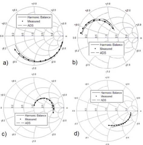
Fig. 6. Matching network for a) source. b) load. Fig. 4. S parameters results in simulation, analysis and
measurements. a) S11 b) S21/5 c) S12x5 d) S22 .
3- 1- 2- Step 2: Designing bias points, Zs and Z1 with considering PA’s linearity
Non-linear HB analysis core presented in section 2-3 , can be done for different bias points, Zs , Zl and input powers. This is done for Vds between 20 to 35 V (1 V steps), Vgs between -3 to 0 V (0.1 V steps), 20 points in a disk around 5 + j50 with radius of 0.2 in Smith chart for Zs, 200 points in a disk around 50 + j20 with radius of 0.5 in Smith chart and input power from 10 dBm to 24 dBm (1 dB intervals).
This alone can be time-consuming process, but with storing results after each analysis and use them as next successive analysis start point, this became faster and took about 30 hours to respond, because each change in states are so small that results are close in two successive analysis.
Bias point, Zs and Zl choosing criterion were output power over 37 dBm and PAE more than 40 % at 1 dB gain compression point. 1 dB gain compression point can be calculated, because of input power sweep for each condition. Zl = 50 + j18 , Zs = 5 + j49, Vds = 30 V and Vgs = -1.1 V were found to be suitable. Source/load impedances at other harmonic was considered zero in this analysis.
3- 1- 3- Step 3: Full search, considering linearity, bandwidth and other harmonics
Zl and Zs impedances at other harmonics are specified with matching networks. 8 two-element transmission line matching network were designed to generate Zl and Zs at fundamental frequency. Analysis done for each combination of these networks (64 pair) and matching network parameters was swept from 90% to 110% (with 5% intervals) of designed value, input power swept from 10 dBm to 24 dBm (with 1 dB steps), Vds from 27 to 33 V (0.5 V steps), Vgs between -1 to -1.3 V (0.05 V steps). Analysis done at different frequencies, 12.4 GHz, 13 GHz and 13.6 GHz. Best performance was seen at Vds = 30 V, Vgs = -1.05 V and matching networks which shown in Fig. 6.
Resulting output power, power gain, and PAE is shown in Fig. 7. Thin line shows analyzed PAE, thick line shows analyzed power gain, dashed line shows analyzed output power and circles shows Agilent ADS simulation results.
Resultant output power was 37.49 dBm, PAE of 47.8% and 22.9 dB power gain at 1 dB gain compression.
3- 2- Power combining
For increasing output power, a number of single transistor
amplifiers were designed to work together and their output powers are combined. Power combining can be performed at three levels. First level is performed at chip or die layer, which is increasing active elements to boost current and output power. Second level is done at circuit level, by power combiner circuits and couplers like Wilkinson, branch-line and Lange couplers. Third level can preformed at space, with some aligned radiative elements. The first and second method can be done in an amplifier design, the third one is done out side of amplifiers.
Power combining in chip is done here, by integrating 12 arms of 125
µ
m periphery device in a chip. Power combining Fig. 7. Single transistor PA design results.Fig. 8. Designed branch-line coupler a) Matching. b) Isolation. c) Amplitude imbalancy.. d) Phase response Maximum
deviation
in circuit level can be done with N-way combiners, which combine N single transistor amplifier outputs together in a single stage, or a three of two way couplers in log2 N stages. With increasing N, N-way combiners have better performance than tree combiners, like lower loss and wider bandwidth, but it is show in [14], for N
≤
8, tree combiners have better performance. For achieving 40 W of output power, 8 single transistor amplifier designed above is needed to combine, so tree combiners are selected. Each combiner has a determined loss from radiation, conductive loss, dielectric loss, dielectric loss and unmatched connections. Phase and amplitude imbalance can also reduce combiner efficiency[15]. If L was total loss for each two way coupler, which made a combiner tree with K layer, total combiner efficiency is [16](15)
2
(1
K)
K
T
L
L
G
η
=
−−
with amplifier block gain G. Eq. (15) shows lower loss, lower layers and higher amplifier gain, result higher efficiency. An effective technique for combining two elements is balanced structure, which may widen amplifier bandwidth to combine bandwidth, improve VSWR, and also combine output powers[17]. This technique needs 90-degree phase shift that is taken form branch-line couplers. After designing balanced amplifier, four balanced amplifiers are combined by a power combiner tree to produce desired output power. Branch-line couplers have flat architecture, suitable for microstripe circuits, and produce 90-degree phase difference at output branches, suitable for balanced amplifier. A branch-line coupler is designed on RT5880 at 13 GHz and simulated using a full wave simulator, namely CST. RT5880 has low loss tangent (0.0009), which would increase efficiency, and low
r (2.2), which will increase circuit dimensions and microstripe accuracy in fabrication process, and results in better phase balance and better efficiency.Designed branch-line results are shown in Fig. 8. Designed coupler has 0.15dB loss, 0.4dB amplitude imbalancy and 3
°
phase imbalancy over desired frequency range, which would be sufficient for this design.form 90 is 3.Two single transistor amplifiers are connected with two similar branch-line couplers and yield a balanced amplifier as shown in Fig. 9. For analysis, CST S-parameters output file for designed branch-line coupler was added to passive linear part in linear-nonlinear separation of elements in Agilent ADS, and new 12
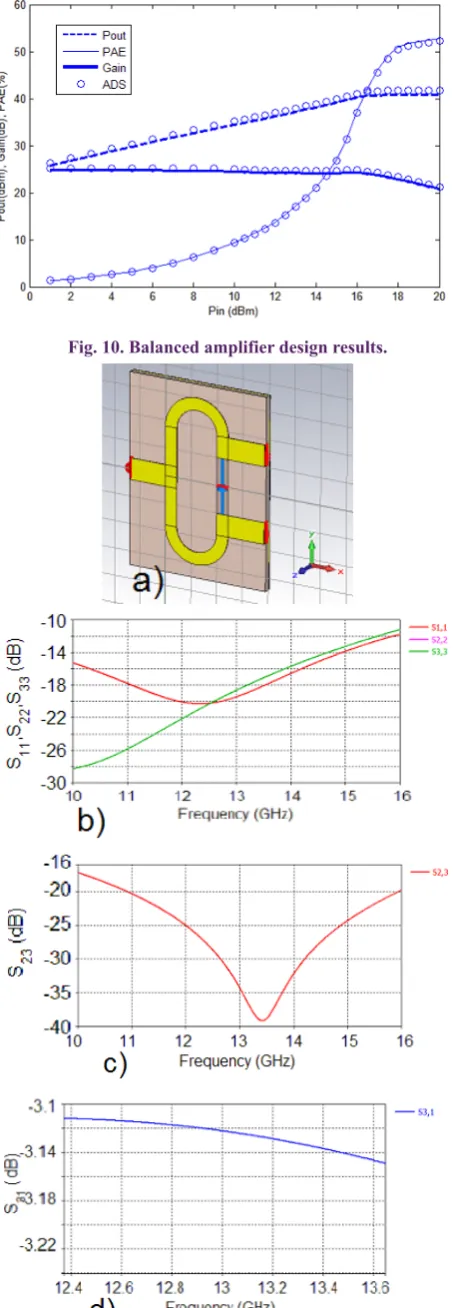
×
12 Y-parameters for linear part was calculated. Harmonic balance analysis, done for structure as shown in Fig. 9, and HB results are shown in Fig. 10. Thin line shows analyzed PAE; thick line shows analyzed power gain, dashed line shows analyzed output power and circles show Agilent ADS simulation results. Maximum output power was 40.63 dBm, PAE was 46.7%, and 23.13 dB power gain was at 1 dB gain compression.For reaching 40 W, at least four balanced amplifier needs to be combined. Maximum combiner loss due to output power would be
(16)
2
(1
K)
K
T
L
L
G
η
=
−−
(17)
10log(
) 0.63
4
desiredbalancedout combiner
out
P
L
dB
P
= −
=
×
Fig. 10. Balanced amplifier design results.Fig. 11. a) Designed Wilkinson power combiner in CST. b) Matching. c) Isolationd) Loss.. 0.15 dB is maximum loss in
Maximum combiner loss due to PAE is
(18) 10log( combiner) 10log( desired ) 0.67
combiner min
balanced PAE
L dB
PAE
η
= − = − =
whichPAEdesired =PAEbalanced×ηcombiner. Combiner loss have to be under 0.63 dB, i.e. the minimum result of equations (16) and (17).
A Wilkinson power combiner is designed and simulated over RT5880 in CST, and output S-parameters file is used in Agilent ADS to generate power combiner tree and, thus, calculate 42
×
42 elements of Y-parameters for this structure. Wilkinson power combiner S-parameters are shown in Fig. 11. As shown in Fig. 11, maximum loss is 0.15 dB, so power combiner tree with two stages is sufficient for producing desired output power and PAE.With using 42
×
42 Y-parameters matrix, total amplifier structure is analyzed. Fig. 12 shows total amplifier results. Thin line shows analyzed PAE, thick line shows analyzed power gain, dashed line shows analyzed output power and circles show Agilent ADS simulation results. Maximum output power was 46.3 dBm, PAE was 43.3% and 21.9 dB power gain at 1 dB gain compression. Fig. 13 a) and b) illustrate Ids for main harmonic and total harmonics, respectively. Fig. 14 a) and b) shows Vds and Vgs for transistors.4- Conclusion
In the presented paper, total designed power amplifier schematics was shown in Fig. 14. Output powers of each
transistor amplifiers and balanced amplifiers are 37.7 dBm and 40.63 dBm, respectively. Output power of first stage Wilkinson’s power combiner reaches at 43.45 dBm and 46.3 dBm at second power combiner stage. With new presented design procedure,a high power (46.3 dBm) and high power added- efficiency (up to 43%) solid state power amplifier at Ku band is designed.
References
[1] M.-S. Lee, D. Kim, S. Eom, H.-Y. Cha, K.-S. Seo, A compact 30-W AlGaN/GaN HEMTs on silicon substrate with output power density of 8.1 W/mm at 8 GHz, IEEE Electron Device Letters, 35(10) (2014) 995-997.
[2] R.C. Fitch, D.E. Walker, A.J. Green, S.E. Tetlak, J.K. Gillespie, R.D. Gilbert, K.A. Sutherlin, W.D. Gouty, J.P. Theimer, G.D. Via, Implementation of High-Power-Density $ X $-Band AlGaN/GaN High Electron Mobility Transistors in a Millimeter-Wave Monolithic Microwave Integrated Circuit Process, IEEE electron device letters, 36(10) (2015) 1004-1007.
[3] T. Torii, S. Imai, H. Maehara, M. Miyashita, T. Kunii, T. Morimoto, A. Inoue, A. Ohta, H. Katayama, N. Yunoue, 60% PAE, 30W X-band and 33% PAE, 100W Ku-band PAs utilizing 0.15 μm GaN HEMT technology, in: 2016 46th European Microwave Conference (EuMC), IEEE, 2016, pp. 568-571.
Fig. 14 a) Vds b) Vgs of transistors over a two-cycle in time domain.
Pin
3 dB
Wilkinson’s power divider
Branch-line
coupler Branch-linecoupler GaN
Amplifier
3 dB
Wilkinson’s power combiner 3 dB
Wilkinson’s power divider
Riso
Riso Riso
Riso
3 dB
Wilkinson’s power combiner
3 dB
Wilkinson’s power divider
Riso
Riso Riso
Riso
3 dB
Wilkinson’s power combiner Rin
RL
Power divider Power combiner
Balanced amplifiers 37.7 dBm
40.63 dBm
43.45 dBm
46.3 dBm
Fig. 15. Total designed power amplifier schematics. Power dividers, balanced amplifiers and power combiners blocks are specified. Fig. 13. Load cycle of transistors. a) main harmonic. b) total
harmonics.
[4] M. Kojima, M. Nagasaka, S. Nakazawa, K. Saito, S. Tanaka, T. Torii, H. Utsumi, K. Yamanaka, 16APSK transmission experiments over 12GHz-band satellite with 100W class GaN power amplifier, in: 2016 Asia-Pacific Microwave Conference (APMC), IEEE, 2016, pp. 1-3.
[5] J.i. Sone, Y. Takayama, Y. Aono, 14-GHz band 1 watt GaAs fet amplifier, Electronics Letters, 15(7) (1979) 212-213.
[6] S.C. Binari, P. Klein, T.E. Kazior, Trapping effects in GaN and SiC microwave FETs, Proceedings of the IEEE, 90(6) (2002) 1048-1058.
[7] A. Zhang, L. Rowland, E. Kaminsky, J. Kretchmer, V. Tilak, A. Allen, B. Edward, Performance of AlGaN/ GaN HEMTs for 2.8 GHz and 10 GHz power amplifier applications, in: IEEE MTT-S International Microwave Symposium Digest, 2003, IEEE, 2003, pp. 251-254. [8] A.H. Jarndal, Large signal modeling of gan device for
high power amplifier design, kassel university press GmbH, 2006.
[9] J.-W. Lee, K.J. Webb, A temperature-dependent nonlinear analytic model for AlGaN-GaN HEMTs on SiC, IEEE Transactions on Microwave Theory and Techniques, 52(1) (2004) 2-9.
[10] W.R. Curtice, M. Ettenberg, A nonlinear GaAs FET model for use in the design of output circuits for power amplifiers, IEEE Transactions on Microwave Theory and Techniques, 33(12) (1985) 1383-1394.
[11] P. Jansen, D. Schreurs, W. De Raedt, B. Nauwelaers, M. Van Rossum, Consistent small-signal and large-signal extraction techniques for heterojunction FET’s, IEEE transactions on microwave theory and techniques, 43(1) (1995) 87-93.
[12] S. Sheppard, K. Doverspike, W. Pribble, S. Allen, J. Palmour, L. Kehias, T. Jenkins, High-power microwave GaN/AlGaN HEMTs on semi-insulating silicon carbide substrates, IEEE Electron Device Letters, 20(4) (1999) 161-163.
[13] J. Wood, D.E. Root, Bias-dependent linear scalable millimeter-wave FET model, IEEE Transactions on Microwave Theory and Techniques, 48(12) (2000) 2352-2360.
[14] A.E. Fathy, S.-W. Lee, D. Kalokitis, A simplified design approach for radial power combiners, IEEE Transactions on Microwave Theory and Techniques, 54(1) (2006) 247-255.
[15] J. Nevarez, G. Herskowitz, Output Power and Loss Analysis of 2/sup n/Injection-Locked Oscillators Combined through an Ideal and Symmetric Hybrid Combiner, IEEE Transactions on Microwave Theory and Techniques, 17(1) (1969) 2-10.
[16] H. Kuno, D.L. English, Millimeter-wave IMPATT power amplifier/combiner, IEEE Transactions on Microwave Theory and Techniques, 24(11) (1976) 758-767.
[17] G. Gonzalez, Microwave transistor amplifiers: analysis and design, Prentice hall New Jersey, 1997.
Pleasecitethisarticleusing:
V. Ezzati and A. Abdipour, Non-linear modeling, analysis, design and simulation of a solid state power amplifier based on GaN technology for Ku band microwave application, AUT J. Model. Simul., 50(2) (2018) 195-202.