Int. J. Adv. Res. Sci. Technol. Volum e 3, Issue 4, 2014, pp.213-218
International Journal of Advanced Research in
Science and Technology
journal homepage: w w w .ijarst.com
IS S N 2319 – 1783 (Print)
IS S N 2320 – 1126 (Online)
Design Of Low Power SRAM Cell Using Area Efficient Leakage Control Technique
J. Harini Nayana*and U. Jyothsna
Department Of ECE, Vizag Institute of Technology, Visakhapatnam, Andhra Pradesh, India.
*Corresponding Author’s Email: [email protected]
A R T I C L E I N F O A B S T R A C T
Article history:
Received Accepted Available online
20 Nov. 2014 19 Dec. 2014 25 Dec. 2014
In deep submicron technologies, leakage power becomes a key for a low power design due to its ever increasing proportion in chip’s total power consumption. Power dissipation is an important consideration in the design of CM OS VLSI circuits. High power consumption leads to reduction in battery life in case of battery powered applications and affects reliability packaging and cooling costs. We propose a technique called LCPM OS for designing CM OS gates which significantly cuts down the leakage current without increasing the dynamic power dissipation. LCPM OS, a technique to tackle the leakage problem in CM OS circuits, uses single additional leakage control transistor, driven by the output from the pull up and pull down networks, which is placed in a path from pull down network to ground which provides the additional resistance thereby reducing the leakage current in the path from supply to ground. The main advantage as compared to other techniques is that LCPM OS technique does not require any additional control and monitoring circuitry, thereby limits the area and also decreases the power dissipation in active state. Along with this, the other advantage with LCPM OS technique is that it reduces the leakage power to an extent of 91.54%, which is more efficient in aspects of area and power dissipation compared to other leakage power reduction techniques.
© 2014 International Journal of Advanced Research in Science and Technology (IJARST). All rights reserved.
Keywords:
Sub threshold leakage current, LCPM OS,
Voltage scaling, LCT,
Self-controlled LCT, Deep-submicron.
Introduction:
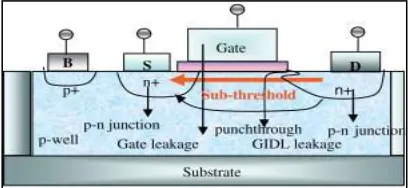
The main sources for power dissipation are: 1) capacitive power dissipation due to the charging and discharging of the load capacitance; 2) s hort-circuit currents due to the existence of a conducting path between the voltage supply and ground for the brief period during which a logic gate makes a transition; and 3) leakage current. The leakage current consists of reverse-bias diode currents and sub threshold currents. The former is due to the stored charge between the drain and bulk of active transistors while the latter is due to the carrier diffusion between the source and drain of the OFF transistors as shown in fig.1.
Digital integrated circuits are found everywhere in modern life and many of them are embedded in mobile devices where limited power resource is available (e.g. mobile phones, watches, mobile computers…). To permit a usable battery runtime, such devices must be designed to consume the lowest possible power. Furthermore, low power is also very important for non -portable devices, too. Indeed reduced power consumption can highly decrease the packaging costs and highly increase the circuit reliability, which is tightly related to the circuit working temperature. Hence, low power consumption is a zero -order
constraint for most ICs manufactured today. In fact, higher performance-per-watt is the new mantra for micro-processor chip manufacturers today. In order to achieve high density and high performance, CMOS technology feature size and threshold voltage have been scaling down for decades. Because of this trend, transistor leakage power has increased exponentially. The reduction of the supply voltage is dictated by the need to maintain the electric field constant on the ever shrinking gate oxide. Unfortunately, to keep transistor speed (proportional to the transistor “on” current) acceptable, the threshold voltage must be reduced too, which results in an exponential increase of the “off” transistor current, i.e. the current constantly flowing through the transistor even when it should be “non-conducting”.
Int. J. Adv. Res. Sci. Technol. Volum e 3, Issue 4, 2014, pp.213-218 As the feature size becomes smaller, shorter
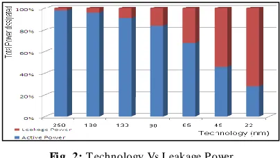
channel lengths result in increased sub -threshold leakage current through a transistor increases when it is off as shown in fig2. Low threshold voltage also results in increased sub-threshold leakage current because transistors cannot be turned off completely. For these reasons, static power consumption, i.e. leakage power dissipation has become a significant portion of total power consumption for current and future silicon technologies .To solve the power dissipation problem, many researchers have proposed different ideas from the device level to the architectural level and above.
Fig. 2: T echnology Vs Leakage Power
In this paper, we describe a new leakage power reduction technique called LCPMOS (Leakage Control PMOS) for designing CMOS circuits. The rest of the paper is organized as follows. Section II describes briefly the prior works on leakage power reduction and their limitations. Section III introduces the transistor models used for estimating the leakage power. Our design strategy and an approach for minimizing the area overhead are described in Sections IV. Results are presented in Section V, followed by conclusions in Section VI respectively.
Limitations with related work:
A. MTCMOS
A high-threshold NMOS gating transistor is connected between the pull-down network and the ground, and low-threshold voltage transistors are used in the gate. The reverse conduction paths exist, which tends the noise margin to reduce or may result in complete failure of the gate. There also exists a performance penalty due to the high-threshold transistors in series with all the switching current paths.
Dual VT technique is a variation in MTCMOS, in which the gates in the critical path use low-threshold transistors and high-threshold transistors for gates in non-critical path [3], [7]. Both the methods requires additional mask layers for each value of VT in fabrication, which is a complicated task depositing two different oxides thickness, hence making the fabrication process complex. The techniques also suffer from turning-on latency i.e., the idle subsections of circuit cannot be used immediately after reactivated since some time is needed to return to normal operating condition. The latency is typically a few cycles for former
method, and for Dual technology, is much higher. When the circuit is active, these techniques are not effective in controlling the leakage power.
B. SLEEP Transistor Technique:
This is a State-destructive technique which cuts off either pull-up or pull-down or both the networks from supply voltage or ground or both using sleep transistors. This technique is MTCMOS, which adds high-Vth sleep transistors between pull-up networks and Vdd and pull-down networks and gnd. while for fast switching speeds, low-Vth transistors are used in logic circuits [8]. Isolating the logic networks, this technique dramatically reduces leakage power during sleep mode. However, the area and delay are increased due to additional sleep transistors. During the sleep mode, the state will be lost as the pull-up and pull-down networks will have floating values. These values impact the wakeup time and energy significantly due to the requirement to recharge transistors which lost state during sleep.
C. Forced Stack:
In this technique, every transistor in the network is duplicated with both the transistors bearing half the original transistor width [6]. Duplicated transistors cause a slight reverse bias between the gate and source when both transistors are turned off. Because sub-threshold current is exponentially dependent on gate bias, it obtains substantial current reduction. It overcomes the limitation with sleep technique by retaining state but it takes more wakeup time
D. ZIGZAG Technique:
Wake-up cost can be reduced in zigzag technique but still state losing is a limitation. Thus, any particular state which is needed upon wakeup must be regenerated somehow. For this, the technique may need extra circuitry to generate a specific input vector.
E. SLEEPY STACK Technique:
This technique combines the structure of the forced stack technique and the sleep transistor technique. In the sleepy stack technique, one sleep transistor and two half sized transistors replaces each existing transistor [10]. Although using of W0/2 for the width of the sleep transistor, changing the sleep transistor width may provide additional tradeoffs between delay, power and area. It also requires additional control and monitory circuit, for the sleep transistors.
F. LEAKAGE Feedback Technique:
Int. J. Adv. Res. Sci. Technol. Volum e 3, Issue 4, 2014, pp.213-218 degradation and increase in area are the limitations
along with the limitation of sleep technique.
G. SLEEPY KEEPER Technique:
This technique consists of sleep transistors connected to the circuit with NMOS connected to Vdd and PMOS to Gnd. This creates virtual power and ground rails in the circuit, which affects the switching speed when the circuit is active [9]. The identification of the idle regions of the circuit and the generation of the sleep signal need additional hardware capable of predicting the circuit states accurately, increasing the area requirement of the circuit. This additional circuit consumes power throughout the circuit operation to continuously monitor the circuit state and control the sleep transistors even though the circuit is in an idle state.
H. LECTOR Technique
This technique consists of two self-controlled transistors which increases the resistance in the path from source to ground, which increases the area of the circuit, one of the most important constraint in the design of vlsi circuits.
LCPMOS:
In this proposed technique, we introduce a single leakage control transistor within the logic gate for which the gate terminal of leakage control transistor (LCT) is controlled by the output of the circuit itself. Which increases the resistance of the path from pull down network to ground thereby increasing the resistance from Vdd to ground, leading to significant decrease in leakage currents. The main advantage as compared to other techniques is that LCPMOS technique does not require any additional control and monitoring circuitry, thereby limits the area and also the power dissipation in active state.
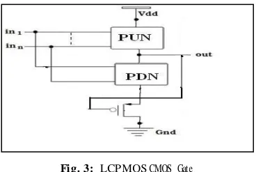
Fig. 3: LCPMOS CMOS Gate
The topology of a LCPMOS CMOS gate is shown in Figure 5. One LCTs are introduced between nodes N1 and Gnd. The gate terminal of LCT is controlled by the output of the circuit itself. As LCT is controlled by output, no external circuit is needed; thereby the limitation with the sleep transistor technique has been overcome. The introduction of LCT increases the resistance of the path from Vdd to Gnd, thus reducing the leakage current.
Fig. 4: LPCMOS based CMOS Inverter
Leakage Control PMOS (LCPMOS) technique is illustrated in detail with the case of an inverter. A LCPMOS INVERTER is shown in Figure 6. A PMOS is introduced as LCT between N1 and Gnd nodes of inverter.
When Vdd = 1V, input A = 0, the output is high. As the output drives the LCT the LCT goes to OFF state hence provides high resistance path between Vdd and Gnd. When A = 1, the output is low; hence LCT will be in ON state hence output is low. LCPMOS inverterfor all possible inputs are tabulated in Table I.
Table: 1. State matrix of LCPMOS inverter
Transistor Reference
Input Vector (A)
0 1
M1 ON State OFF State
M2 OFF State ON State
LCT Near Cut-OFF
State ON State
In the sleep related technique, the sleep transistors have to be able to isolate the power supply and/or ground from the rest of the transistors of the gate. Hence, they need to be made bulkier dissipating more dynamic power. This offsets the savings yielded when the circuit is idle. Sleep transistor technique depends on input vector and it needs additional circuitry to monitor and control the switching of sleep transistors, consuming power in both active and idle states. In comparison, LCPMOS generates the required control signals within the gate and is also vector independent.
Single transistor is added in LCPMOS technique in every path from Vdd to Gnd irrespective of number of transistors in pull-up and pull-down network. Whereas, forced stacks have 100% area overhead. The loading requirement with LCT is a constant which is much lower.
Applying LCPMOS to CMOS Circuits:
Int. J. Adv. Res. Sci. Technol. Volum e 3, Issue 4, 2014, pp.213-218
A. LCPMOS based NOT gate:
Fig. 5: 2-input LCPMOS NOT
Fig. 6: Simulation waveforms of LCPMOS NOT
The CMOS INVERTER is shown in Figure5 with the one LCT added between pull-down networkand gnd. The simulation waveforms of LCPMOS NOT from Figure 8 show that the basic characteristics of NOT are retained by LCPMOS NOT.
B. LCPMOS based NAND gate:
Fig. 7: 2-input LCPMOS NAN D
Fig. 8: Simulation waveforms of LCPMOS NAND
The 2-input CMOS NAND gate is shown in Figure 7 with the one LCT added between pull-down network and gnd. The simulation waveforms of LCPMOS NAND from Figure 8 show that the basic characteristics of NAND are retained by LCPMOS NAND.
C. LCPMOS based NOR gate:
Fig. 9: 2-input LCPMOS NOR
Fig. 10: Simulation waveforms of LCPMOS NOR
The 2-input CMOS NOR gate is shown in Figure 8 with the one LCT added between pull-down network and gnd. The simulation waveformsof LCPMOS NOR from Figure 8 show that the basic characteristics of NOR are retained by LCPMOS NOR.
D. LCPMOS based AOI gate:
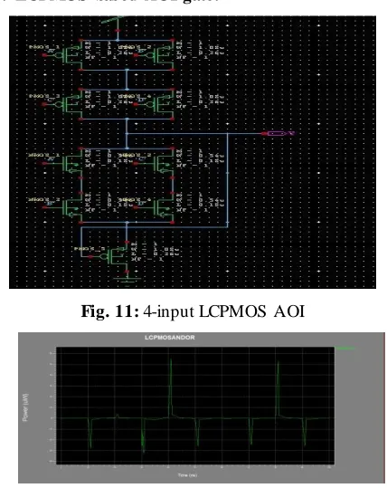
Fig. 11: 4-input LCPMOS AOI
Fig. 12: Simulation waveforms of LCPMOS AOI
Int. J. Adv. Res. Sci. Technol. Volum e 3, Issue 4, 2014, pp.213-218
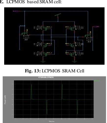
E. LCPMOS based SRAM cell:
Fig. 13: LCPMOS SRAM Cell
Fig. 14: Simulation waveforms of LCPMOS NOR
The CMOS SRAM cell gate is shown in Figure.13 with the one LCT added between pull-down network and gnd. The simulation waveforms of LCPMOS SRAM Cell from Figure.14 show that the basic characteristics of SRAM Cell are retained by SRAM Cell.
Experimental Results:
The leakage power is measured using the S-EDIT simulator. The results obtained through the technique for NOT gate is shown in Table III. Simulation for the 2-input NOT is performed by taking three different process parameters Viz. 180nm, 90nm.
Table: 2. NOT results for various technologies
Technology Leakage Power (uW)
CMOS LECTOR LCPMOS
180nm 100 90 30
90nm 660 60 51
Table: 3. NAND Results for Various Technologies
Technology Leakage Power (uW)
CMOS LECTOR LCPMOS
180nm 105 80 30
90nm 600 64 50
Table: 4. NOR results for various technologies
Technology Leakage Power (uW)
CMOS LECTOR LCPMOS
180nm 56 29 13
90nm 490 110 100
Table: 5. AOI Results for Various Technologies
Technology Leakage Power (uW)
CMOS LECTOR LCPMOS
180nm 140 120 55
90nm 720 110 80
Table: 6. SRAM Results for Various Technologies
Technology Leakage Power (uW)
CMOS LECTOR LCPMOS
180nm 8.5 2 1.5
90nm 1.2 41 3.6
Leakage power dissipation is taken as the average of power dissipations obtained at all the possible input vectors of the CMOS circuit. There are 4 possible combinations for 2-input NAND, hence the average of the four power dissipations gives the leakage power. In each case, the leakage power is measured by exciting the circuits f o r 3 c a s e s (Conventional and LECTOR and LCPMOS) with same set of input vectors.
Conclusion:
The increase in leakage power because of the scaling down of device dimensions, supply and threshold voltages in order to achieve high performance and low dynamic power dissipation, becomes more with the deep-submicron and nanometer technologies and thus it becomes a great challenge to tackle the problem of leakage power. LCPMOS uses one LCT which is controlled by the output of circuit itself. LCPMOS achieves the reduction in leakage power compared to other leakage reduction techniques, such as LECTOR, sleepy stack, sleepy keeper, etc, along with the advantage of not affecting the dynamic power, since this technique does not require any additional control and monitor circuitry and also in this technique, the exact logic state is maintained. The LCPMOS technique when applied to generic logic circuits achieves up to 80-92% leakage reduction over the respective conventional circuits without affecting the dynamic power. A tradeoff between Propagation delay and area overhead exists here.
References:
1.P. Verma, R. A. M ishra, “Leakage power and delay analysis of LECTOR based CM OS circuits”, Int’l conf. on computer & communication technology ICCCT 2011.
2.H. Narender and R. Nagarajan, “LECTOR: A technique for leakage reduction in CM OS circuits”, IEEE trans. on VLSI systems, vol. 12, no. 2, Feb. 2004.
3.L. Wei, Z. Chen, M . Johnson, and K. Roy, “Design and optmization of low voltage high performance dual threshold CM OS circuits,” in Proc. 35th DAC, 1998, pp.489–492.
4.John F. Wakerly, “Digital Design- Principles and Practices”, fourth edition.
Int. J. Adv. Res. Sci. Technol. Volum e 3, Issue 4, 2014, pp.213-218
Roy, “Leakage control with efficient use of transistor stacks in single threshold CM OS,” IEEE Trans. VLSI Syst., vol. 10, pp. 1–5, Feb. 2002.
6.B. S. Deepak subramanyan, A. Nunez, “Analysis of sub threshold leakage reduction in CM OS digital circuits,” in Proc. 13th NASA VLSI Symp.,June 2007.
7.Q. Wang and S. Vrudhula, “Static power optimization of deep sub-micron CM OS circuits for dual VT technology,” in Proc. ICCAD, Apr. 1998, pp.
490–496.
8.M . D. Powell, S. H. Yang, B. Falsafi, K. Roy, and T. N. Vijaykumar, “Gated-Vdd: A ciruit technique to reduce leakage in deep submicron cache memo ri es ,” in Proc. IEEE ISLPED, 2000, pp. 90-95. 9.S. H. Kim and V. J. M ooney, “Sleepy Keeper: a
new approach to low-leakage power VLSI design,” IFIP, pp.367-372, 2006.