Guideline on Quantitatively Analyzing Analog
Nano-Scale CMOS Circuits Using Ultra-Compact Model
Haoran Yu*, Kamal El-Sankary, Ezz El-Masry
Department of Electrical and Computer Engineering, Dalhousie University, Halifax, Canada
Abstract
This paper presents a tutorial about analyzing analog nano-scale CMOS circuits quantitatively. A ultra-compact model which is numerically accurate is essential in the analysis. Besides, the characteristics of nano-scale MOSFET must be considered. The nonlinear output conductance and the cross-terms among the controlling voltage cannot be ignored in nano-scale circuits. Distortion analysis of nano-scale gate-driven and bulk-driven amplifier is performed as a demonstration of this guideline.Keywords
CMOS, Bulk-driven, Distortion, Model1. Introduction
Owing to the reducing channel length of metal – oxide – semiconductor field-effect transistor (MOSFET), the performance of complementary metal-oxide-semiconductor (CMOS) integrated circuits (IC) has been improved greatly, such as power consumption, speed and noise [1-3]. Meanwhile, bulk-driven (BD) technique has been proposed to tackle the harsh voltage-swing challenge in modern low voltage design [4]. BD MOSFET works in a depletion mode which allows negative, zero and small positive bias voltage at the bulk terminal. This technique increases the input common mode range as well as the signal swing, which cannot be realized by gate-driven (GD) technique at low VDD
[4].
To design high performance nano-scale GD/BD circuits, quantitative analysis is necessary. In order to analyze nano-scale circuits quantitatively, firstly, a current model which characterizes transistor accurately is demanded. Especially for BD circuits, the model must be also accurate when the signal is applied at the bulk-terminal.
To describe the characteristics of nanometer MOSFET, several physic effects have to be included into model, such as the short-channel (SCE) and the narrow width effect (NWE), the mobility degradation (MD), the velocity saturation (VS), the channel-length modulation (CLM), the drain-induced barrier lowering (DIBL) and the source-drain parasitic r es is tan ce ( S /D - P R) [ 5 ]. Ber k el e y sh o r t - ch an ne l insulated-gate model (BSIM) [6] provides the highest accuracy; however, it has a large number of parameters and
* Corresponding author: [email protected] (Haoran Yu)
Published online at http://journal.sapub.org/msse
Copyright © 2014 Scientific & Academic Publishing. All Rights Reserved
is the most complex model which is simulation-oriented, not suitable for circuit analysis. Comparing with simulation-oriented model, ultra-compact model is more ideal to be applied to analyze circuit [5].
Models can be also selected according to the type of analysis, i.e. qualitative or quantitative analysis. For qualitative analysis, simple model can be used as long as it shows the characteristics of MOSFET in the targeting operational region qualitatively accurately. For example, the model from [7] that covers the subthreshold and moderate inversion regions was successfully applied to analyze the mixing mechanism of BD mixer and new application of BD mixer has been found based on the analysis [8].
For quantitative analysis, such as the numerical calculation of distortion of nanometer GD/BD circuits, ultra-compact model which is numerically accurate for nano-scale MOSFET must be chosen. Reference [5] provides such a model which has ten parameters and is accurate for nanometer MOSFET; however, it was originally proposed to digital applications, not optimized for bulk-driven applications. In this work, the model is modified to be adapted to the characteristics of nano-scale BD transistor. Hence it can be applied to quantitatively analyze BD circuits.
Besides the model selection/adaption, the characteristic of nano-scale MOSFET must be also considered in the analysis. In this research, it is found that the nonlinear output conductance and the cross-terms play important roles in the analysis, although they are often ignored in the analysis of mirco-scale CMOS circuits.
Section 3 shows the importance of the inclusion of the nonlinear output conductance and the cross-terms. The distortion analysis of GD/BD RF amplifier is demonstrated as an example of this guideline. Finally there is a brief conclusion in Section 4.
2. Accurate Current Model for
Nano-Scale MOSFET and Its
Modification for BD Applications
2.1. Original Current Model
By combining the merits of the previous ultra-compact models [9-12], and by including DIBL, NWE, and S/D-PR, a 10-parameter model was proposed for nano-scale CMOS transistor in [5]:
𝑖𝑑𝑠 = 𝑖𝐷0 1+𝑅𝐷𝑆 0∙𝑖𝐷0
𝜛 ∙𝑣𝐷𝑆
(1) where
𝑖𝐷0= 𝜛𝐶𝐼 𝑣𝐺𝑆− 𝑉𝑡 𝑛 1 + 𝜆 𝑣𝐷𝑆− 𝑉𝐷𝑆𝐴𝑇 , (2)
𝑉𝐷𝑆𝐴𝑇 = 𝐶𝑉 𝑣𝐺𝑆− 𝑉𝑡 𝑎, (3)
𝑉𝑡= 𝑉𝑡0+𝜂𝑁𝑊𝐸𝜛 − 𝜂𝐷𝐼𝐵𝐿𝑣𝐷𝑆+ 𝜂𝐵𝐵𝑣𝑆𝐵. (4)
𝐶𝐼 and 𝐶𝑉 are used to linearly proportionally scale
current and saturation voltage; n and a are used to describe the fractional power dependence of the current and the saturation voltage on the overdrive voltage 𝑣𝐺𝑆− 𝑉𝑡 ;
body biasing (BB), DIBL, and NWE are described by adding corrective terms 𝜂𝐵𝐵, 𝜂𝐷𝐼𝐵𝐿 𝑎𝑛𝑑 𝜂𝑁𝑊𝐸 into 𝑉𝑡 ; the
transistor width is referred as is the multiple, 𝜛, of the minimal allowed width; 𝑅𝐷𝑆0 is used to describe the impact
of S/D-PR; 𝜆 is the coefficient of CLM.
This model describes the I-V characteristics accurately in superthreshold region [5]. However, it was originally proposed to digital applications, not optimized for BD applications. In order to perform the quantitative analysis of BD circuits, it is modified in this work to adapt to BD MOSFET and the parameters are fitted to a commercial 65 nm technology used in this research.
2.2. Modified Model for BD Applications
To investigate if the model can describe the characteristics of nano-scale MOSFET accurately, I-V characteristic needs to be examined. Furthermore, up-to-three order of derivatives 𝐾𝑙𝑚𝑛 of 𝑖𝑑𝑠 over bias voltages have to be fitted.
𝐾𝑙𝑚𝑛 is defined as:
𝐾𝑙𝑚𝑛 =
𝑙!1𝑚!1 𝑛!1𝜕𝑣𝜕 𝑙+𝑚 +𝑛 𝑔𝑠𝑙 𝜕𝑣 𝑖𝑑𝑠 𝑠𝑏 𝑚𝜕𝑣
𝑑𝑠𝑛 𝑣𝑣𝑔𝑠=𝑉𝐺𝑆 𝑠𝑏=−𝑉𝐵𝑆 𝑣𝑑𝑠=𝑉𝐷𝑆
when 𝑙 ≠ 0 or 𝑛 ≠ 0
−1 ∙ 1 𝑚!
𝜕𝑚𝑖𝑑𝑠 𝜕𝑣𝑠𝑏𝑚
𝑣𝑠𝑏=−𝑉𝐵𝑆
when 𝑙 = 𝑛 = 0
(5) 𝑙 + 𝑚 + 𝑛 ∈ 1,2,3 , and 𝑙, 𝑚, 𝑛 ∈ 𝑁.
Obviously, 𝐾100= 𝑔𝑚 𝐾010= 𝑔𝑚𝑏, and 𝐾001= 𝑔𝑜 ,
which are the first-order coefficients of the nonlinear (bulk-) transconductance and the nonlinear output conductance,
respectively. 𝐾200, 𝐾300 , 𝐾020, 𝐾030 , and 𝐾002, 𝐾003
are second- and third-order nonlinear coefficient only related to 𝑣𝑔𝑠 , 𝑣𝑠𝑏 , and 𝑣𝑑𝑠 , respectively. Others are the
coefficients of the cross-terms among 𝑣𝑔𝑠, 𝑣𝑠𝑏, and 𝑣𝑑𝑠.
In strong inversion region, 𝐶𝐼, 𝑛, 𝐶𝑉 and 𝑎 are the most
effective parameters to adjust 𝐼𝐷 and (𝐾100, 𝐾200 and 𝐾300)
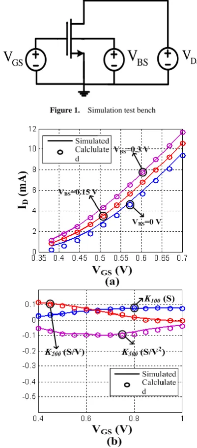
versus 𝑉𝐺𝑆. Figure 2 shows the results of parameter fitting.
Figure 2 (a) shows the drain current 𝐼𝐷 versus 𝑉𝐺𝑆 when
𝑉𝐷𝑆= 0.5 V . Figure 2 (b) shows 𝐾100, 𝐾200 and 𝐾300
versus 𝑉𝐺𝑆 when 𝑉𝐷𝑆= 1 V and 𝑉𝐵𝑆 = 0 V . The
simulation data are obtained from a transistor of 𝑊 𝐿 = 60𝜇𝑚 80𝑛𝑚, using BSIM 4 model; The simulation test bench is shown in Figure 1.
GS
V
V
BSV
DSFigure 1. Simulation test bench
Figure 2. Comparison between the simulated and calculated 𝐼𝐷 and
(𝐾100, 𝐾200 and 𝐾300) versus 𝑉𝐺𝑆
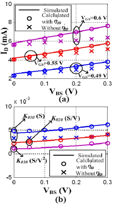
𝐼𝐷 and (𝐾001, 𝐾002 and 𝐾003) versus 𝑉𝐷𝑆 are mainly
saturation region. Figure 3 demonstrates the comparison of 𝐼𝐷 and (𝐾001, 𝐾002 and 𝐾003) versus 𝑉𝐷𝑆. In Figure 3 (a),
𝑉𝐵𝑆 = 0 V. In Figure 3 (b) 𝑉𝐺𝑆 = 0.5 V and 𝑉𝐵𝑆 = 0 V.
From Figure 2 and Figure 3 show that good fitting of 𝑖𝑑𝑠 and
its derivatives over 𝑉𝐺𝑆 and 𝑉𝐷𝑆 are achieved.
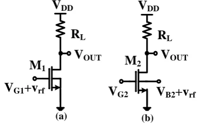
In the original model, 𝐼𝐷 and (𝐾010, 𝐾020 and 𝐾030) are
basically adjusted by 𝑛 and 𝜂𝐷𝐼𝐵𝐿. It is found for the
original model in [5] that even if the calculated 𝐾020 and 𝐾030 are close to the simulated values, 𝐼𝐷 and
𝐾010 are still underestimated. And if 𝐼𝐷 and 𝐾010 are
adjusted to be close to the simulated ones, 𝐾020 and 𝐾030
are apart from the simulated values. It is proposed that −𝜂𝐵𝐵′ 𝑣𝑆𝐵 is added to the current model to adjust 𝐼𝐷 and
𝐾010 without affecting 𝐾020 and 𝐾030:
𝑖𝑑𝑠 = 𝑓 𝑣𝑔𝑠, 𝑣𝑠𝑏, 𝑣𝑑𝑠 𝑜𝑟𝑖𝑔𝑖𝑛𝑎𝑙𝑖𝑛 [12]− 𝜂𝐵𝐵′ 𝑣𝑠𝑏. (5)
Figure 4 illustrates the result of the parameter-fitting by comparing 𝐼𝐷 and (𝐾010, 𝐾020 and 𝐾030) versus 𝑉𝐵𝑆. In
Figure 4 (a), 𝑉𝐷𝑆= 0.5 V. In Figure 2 (b), 𝑉𝐷𝑆= 0.4 V and
𝑉𝐺𝑆 = 0.5 V. It is clear that without this added parameter, 𝐼𝐷
and 𝐾010 are underestimated. This added parameter gives
us one more degree of freedom to achieve accurate fitting of both linear and nonlinear terms.
Figure 3. Comparison between the simulated and calculated 𝐼𝐷 and (𝐾100, 𝐾200 and 𝐾300) versus 𝑉𝐺𝑆
Figure 4. Comparison between the simulated and calculated 𝐼𝐷 and
(𝐾010, 𝐾020 and 𝐾030) versus 𝑉𝐵𝑆
Although in the range of 𝑉𝐵𝑆 = 0 to 0.1 V, 𝐼𝐷 is still
underestimated (as shown in Figure 2 (a), Figure 3 (a), and Figure 4 (a)) and 𝐾010 is a little overestimated (as shown in
Figure 4 (4)), the fitting parameters can give us reasonable accuracy in quantitative analyses. A current model which is fitted to the used technology accurately is the prerequisite of numerically analyzing nano-scale CMOS circuits.
3. Quantitative Analysis of Nano-Scale
Circuits
distortions, and the distortions can be acquired as the outputs [13-15].
Figure 5. Schematic of GD amplifier (a), and BD amplifier (b)
It is imperative to acknowledge that the output conductance and the cross-terms among the controlling voltages must be included in the quantitative analysis of nano-scale CMOS circuits, although for the distortion analysis of GD CMOS circuits in micrometer scale, their effects were often ignored [13, 16, 17]. It is found that this exclusion would cause serious distortion calculation error in the analysis of deca-nano scale CMOS circuits and the failure to predict the effect of the increasing of the overdrive voltage and the source degeneration resistance, even if this accurate model is used in the analytical calculation. This can be demonstrated in Figure 6 to Figure 9, showing the value of harmonic distortion (HD) of GD and BD RF amplifier in a 65 nm technology, respectively. The GD/BD amplifier is shown in Figure 5, both of which have the size of 𝑊 𝐿 = 60 μm 80 nm, 𝑅𝐿= 400 Ω and 𝑣𝑟𝑓 = 1 𝑚V@2 GHz.
The the expression of HD2 and HD3 of the GD and BD
amplifier can be found in [14, 15], respectively.
From Figure 6, it is clear that there is significant error between the simulated and the calculated second-order and third-order harmonic distortion (HD2 and HD3) if only the
nonlinearity of the transconductance is considered in the analytical calculation. The calculation cannot even predict the trend of behavior of HD. It is also found that the effect of the source degeneration resistance (RS) depends on the bias
point in this study. Under certain bias condition, the increase of RS cannot reduce HD monotonically, as shown in Figure 7,
where the bias current is 3.2 mA. However, if the contribution from the nonlinear output conductance and the cross-terms is excluded, the nonlinear term only from the transconductance is reducing continuously with RS, i.e. the
value of 𝑔 𝐾200
𝑚(1+𝑔𝑚𝑅𝑆)2 (𝑉
−1) and 𝐾300
𝑔𝑚(1+𝑔𝑚𝑅𝑆)−
2𝐾2002 𝑅𝑆
𝑔𝑚 1+𝑔𝑚𝑅𝑆 4 (𝑉
−2)
.
Similar finding is made in nano-scale BD amplifier as shown in Figure 8 and Figure 9. Figure 8 shows substantial error exits if the nonlinearity of the output conductance and the cross-terms are excluded. In Figure 9 (a), taking only the nonlinearity from the body-transconductance into consideration will overestimate the effect of RS on HD2.
Nearly 20 dB reduction of HD2=12𝑉𝑖𝑛 𝐾020𝐺𝑆 2
𝐺𝑆+𝑔𝑚𝑏 2𝑔𝑚𝑏 is
expected if only the nonlinearity from the body-transconductance is considered; however, only about 6 dB reduction is obtained by simulation. For HD3, simulation
shows that at this bias condition (the bias current is 2.5 mA), RS cannot be used to reduce HD3; however, calculation of the
term that only includes the nonlinearity of the body - transconductance, i.e. 𝐾030 𝐺𝑆+𝑔𝑚𝑏 𝐺𝑆
3−2𝐾 0202 𝐺𝑆3
𝐺𝑆+𝑔𝑚𝑏 4 𝑉
−2
shows an opposite change of HD3 with RS, as shown in
Figure 9 (b). Here, 𝐺𝑆= 𝑅𝑆 −1.
Figure 6. Comparison of the simulated HD2 (a) and HD3 (b) versus VGS of the nano-scale GD amplifier with the calculated HD which only includes the
nonlinearity of the transconductance
V
B2+v
rfR
LV
OUTV
G2V
DDM
2V
G1+v
rfR
LV
OUTV
DDM
1Figure 7. Comparison of the simulated HD2 (a) and HD3 (b) versus the source degeneration resistance of a nano-scale GD amplifier with the calculated HD
which only includes the nonlinearity of the transconductance
Figure 8. Comparison of the simulated HD2 (a) and HD3 (b) versus VGS of thenano-scale GD amplifier with the calculated HD which only includes the
nonlinearity of the transconductance
Figure 9. Comparison of the simulated HD2 (a) and HD3 (b) versus the source degeneration resistance of a nano-scale GD amplifier with the calculated HD
Therefore, for nano-scale CMOS circuit, the effect of the nonlinear output conductance and the cross-terms must be included; otherwise the distortion analysis is far from being accurate, based on which the linearization techniques are not practical.
On contrast, by including the output conductance and the cross-terms, using this modified ultra-compact model, calculation gives good agreement with the simulation result.Moreover, the distortion behavior can beinterpreted quantitatively owing to the accurate ultra-compact model. Next, HD3 of the GD amplifier and HD2 of the BD amplifier
are analyzed as demonstrations [14, 15].
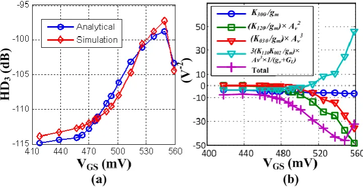
Figure 10 (a) and Figure 11 (a) shows that by using the modified model, the analytical calculation which includes the effects of the output conductance and the cross-terms provides satisfactory accuracy, comparing with the simulation. Furthermore, by analyzing the dominant terms in
the HD3expression, the trend of HD3 can be interpreted in
Figure 10 (b). It is found that 𝐾300/𝑔𝑚 increases
continuously. Besides, when 𝑉𝐺𝑆 > 480 𝑚𝑉, 𝐴𝑣2(𝐾120/
𝑔𝑚) , 𝐴𝑣3(𝐾003/𝑔𝑚) , and 3𝐴𝑣2(𝐾002𝐾110/𝑔𝑚)(1/𝑔𝑜+
𝐺𝐿) increase substantially and become the major parts of
HD3; also, the last one has opposite sign against the first two,
thus the total of them, i.e. HD3, shows the characteristic
shown in Figure 10. Here, 𝐴𝑣= 𝑔𝑚/(𝑔𝑜+ 𝐺𝐿), 𝑔𝑜is the
output conductance and 𝐺𝐿 is the load. From Figure 11 (b),
it is realized that although the amplitude of the 𝐾300- and
𝐾200-related term is monotonically reduced by 𝑅𝑆, the
amplitude of the 𝐾210-, 𝐾120-, and 𝐾003- related terms is
parabola, especially the 𝐾120-related term becomes the major
part when 𝑅𝑆> 60 Ω. Thus, the total of all the terms in
HD3 behaves as parabola and starts increasing when 𝑅𝑆>
60 Ω.
Figure 10. (a) Analytical and simulated HD3, and (b) 𝐾030/𝑔𝑚𝑏, three other major contributions, and the sum of all the terms in HD3
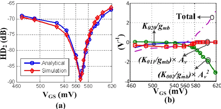
Figure 12. (a) Analytical and simulated HD2 when 𝑉𝐵𝑆= 0 V, and (b) the contribution of each term and the sum of all the terms in HD2
Figure 13. 𝐾020 and 𝐾110-related terms in HD2 and the total of all the terms in HD2 versus 𝑅𝑆 under 2.5mA bias current and 𝑉𝐵𝑆= 0 V
Similarly, for the BD amplifier, after taking into account the output conductance and the cross-terms, good accuracy is achieved in the calculation using this model, as shown in Figure 12 (a) and Figure 13 (a). Figure 12 (b) explains the behavior of HD2 of the BD amplifier: 𝐾020/𝑔𝑚𝑏 contributes
less as VGS increases; however, −𝐴𝑣2(𝐾002/𝑔𝑚𝑏) increases
significantly when 𝑉𝐺𝑆≥ 560 mV, thus 𝐻𝐷2 is increased.
Moreover, the contribution of −𝐴𝑣2(𝐾002/𝑔𝑚𝑏) cancels that
of 𝐴𝑣(𝐾011/𝑔𝑚𝑏) since they have the same sign and
subtract each other. The values of the two terms are equal around 𝑉𝐺𝑆 = 566 mV, hence there is an optimal region of
HD2. Figure 13 (b) demonstrates the contribution of
𝐾020 and 𝐾110 -related terms in HD2 . Although 𝐾020
contributes less as well known in long channel technology, the contribution of 𝐾110-related term increase significantly
and counteract against the reduction of 𝐾020-related term.
Thus HD2 reduces slower as 𝑅𝑆 increases.
By following this guideline, i.e. using an quantitatively accurate model and including the nonlinear output conductance and the cross-terms, HD2 of the GD amplifier
and HD3 of the BD amplifier can be calculated correctly and
each term in the expressions of HD2/HD3 can be analyzed to
interpret the characteristic.
4. Conclusions
The guideline of quantitatively analysing nano-scale CMOS circuits can be summarized as:
First, anultra-compact model which is numerically accurate for nano-scale MOSFET is required. The parameters in the model have to be fitted the used technology. One of these kinds of models is introduced in this paper, which is modified here to be adapted to BD applications by introducing one new parameter to achieve accurate fitting of both linear and nonlinear terms. This modified model can be applied for analysing nano-scale GD/BD circuits.
Second, for nano-scale CMOS circuits, the nonlinear output conductance and the cross-terms among the controlling voltages, i.e. 𝑣𝑔𝑠 , 𝑣𝑠𝑏, and 𝑣𝑑𝑠, must be
included; otherwise there would be significant error between the calculated and simulated results.
BD amplifier is demonstrated as an example to show the importance of the nonlinear output conductance and the cross-terms, as well as the effectiveness of the accurate ultra-compact model.
REFERENCES
[1] B. Razavi, Design of Analog CMOS Integrated Circuits, 1st ed. Boston, MA: McGraw-Hill, 2000.
[2] T.H. Ning, "Directions for silicon technology as we approach the end of CMOS scaling," in Proc. IEEE Conf. Solid-State Inte. Circuit Tech. (ICSICT), Shanghai, China, Nov. 2010, pp. 3-3.
[3] I.A. Young, "Analog mixed-signal circuits in advanced nano-scale CMOS technology for microprocessors and SoCs," in Proc. IEEE European Solid-State Circuits Conf. (ESSCIRC)<br />, Seville, Spain, Sep. 2010, pp. 61-70. [4] B.J. Blalock, P.E. Allen and G. Rincon-Mora, "Designing
1-V op amps using standard digital CMOS technology," IEEE Trans. Circuits Syst. II, Analog Digit. Signal Process., vol. 45, no. 7, pp. 769-780, 1998.
[5] E. Consoli, G. Giustolisi and G. Palumbo, "An accurate ultra-compact I–V model for nanometer MOS transistors with applications on digital circuits," IEEE Trans. Circuits Syst. I, Reg. Papers, vol. 59, no. 1, pp. 159-169, 2012.
[6] T. Morshed , W. Yang , M. Dunga , X. Xi , J. He , W. Liu , Kanyu , M. Cao , X. Jin , J. Ou , M. Chan , A. Niknejad and C. Hu. BSIM4.6.4 MOSFET model [Online]. available: http://www-device.eecs.berkeley.edu/~bsim3/BSIM4/BSIM 464/BSIM464_Manual.pdf.
[7] B. Toole, C. Plett and M. Cloutier, "RF circuit implications of moderate inversion enhanced linear region in MOSFETs," IEEE Trans. Circuits Syst. I, Reg. Papers, vol. 51, no. 2, pp. 319-328, 2004.
[8] Haoran Yu, K. El-Sankary, and E. El-Masry, "A methodology to design bulk-driven mixer with harmonic mixing rejection," Analog Integrated Circuits and Signal Processing, vol. 77, no. 3, pp. 503-511, 2013.
[9] T. Sakurai and A.R. Newton, "Alpha-power law MOSFET model and its applications to CMOS inverter delay and other formulas," IEEE J. Solid-State Circuits, vol. 25, no. 2, pp. 584-594, 1990.
[10] T. Sakurai and A.R. Newton, "A simple MOSFET model for circuit analysis," IEEE Trans. Electron Devices, vol. 38, no. 4, pp. 887-894, Apr. 1991.
[11] M.M. Mansour, M.M. Mansour and A. Mehrotra, "Modified Sakurai-Newton current model and its applications to CMOS digital circuit design," in Proc. IEEE Comput. Society Annu. Symp. VLSI, Tampa, Florida, Feb. 2003, pp. 62-69.
[12] N. Chandra, A. Kumar Yati and A.B. Bhattacharyya, "Extended-Sakurai-Newton MOSFET model for ultra-deep- submicrometer CMOS digital design," in Proc. Int. Conf. VLSI Design, New Delhi, India, Jan. 2009, pp. 247-252.
[13] R.A. Baki, T.K.K. Tsang and M.N. El-Gamal, "Distortion in RF CMOS short-channel low-noise amplifiers," IEEE Trans. Microw. Theory Tech., vol. 54, no. 1, pp. 46-56, Jan. 2006.
[14] Haoran Yu, K. El-Sankary, and E. El-Masry, "Distortion analysis of nano-scale CMOS RF amplifier using Volterra series," in Proc. of Canadian Conf. Electrical and Computer Engineering (CCECE), Toronto, Canada, May, 2014, pp. 1-4.
[15] Haoran Yu, K. El-Sankary, and E. El-Masry, "Distortion analysis using volterra series and linearization technique of nano-scale bulk-driven CMOS RF amplifier," IEEE Trans. Circuits Sys. I: Reg. Papers, accepted.
[16] R.A. Baki, T.K.K. Tsang and M.N. El-Gamal, "Distortion in RF CMOS short channel low noise amplifiers," in Proc. IEEE Int. NEWCAS Conf., Jun. 2005, pp. 369-372.