Metallurgy and Kinetics of Liquid–Solid Interfacial Reaction
during Lead-Free Soldering
Jin Liang
1;*, Nader Dariavach
1, Paul Callahan
1and Dongkai Shangguan
21
EMC, Hopkinton, Massachusetts, 01748 USA
2Flextronics, San Jose, California, 95131 USA
The wetting of a molten solder on metallic surfaces is a rather complex phenomenon. In addition to physical spreading due to surface tension reduction, there are interfacial metallurgical and flux chemical reactions with the metallic substrate surface. Substrate dissolution and intermetallic formation take place rapidly during soldering. Since lead-free soldering requires substantially higher soldering temperatures (around 250C), the rates of intermetallic growth and substrate dissolution for lead-free solders are expected to be significantly greater than those
for the current Sn–Pb eutectic solder. This study systematically investigates the metallurgy of the solid–liquid interface reactions and intermetallic growth kinetics for three lead-free solders: Sn–Ag eutectic (96.5%Sn–3.5%Ag), Sn–Cu eutectic (99.3%Sn–0.7%Cu) and Sn–Ag– Cu eutectic (Sn–3.8Ag–0.7Cu, SAC 387) with three metallic substrates: Cu, Ni, and Alloy 42 (42%Ni–52%Fe) over temperatures ranging from 225 to 280C for reaction time from 10 s to 16 h. Wetting behavior of these three alloys on PCBs with OSP, immersion Sn, and Ni/Au finishes,
was also examined from 220C up to 260C. A thorough understanding of lead-free solder/substrate interfacial reactions should give guidance
to the optimum lead-free soldering processes and to the optimum lead-free coating thicknesses for component and PCB terminal finishes, as well as for under-chip metallurgical coatings for flip-chip and BGA applications.
(Received June 27, 2005; Accepted November 15, 2005; Published February 15, 2006)
Keywords: lead-free, wettability, intermetallic kinetics, PCB board finish
1. Introduction
Understanding wettability, metallurgy, and intermetallic growth kinetics at the solid–liquid interface is essential for a robust soldering process and for long term reliability of electronic products. Factors, such as the conditions of the metallic surfaces (i.e., the nature of any oxides or other coating or films, surface roughness), temperature distribution during the soldering, as well as the fundamental interfacial metallurgical and flux chemical reactions with the metallic surface, all play important roles in determining the final solder spreading/wetting. The degree of solder spread and wetting determine the final shape/geometry of solder joint interconnect, and the mechanical strength and reliability of the joints and assemblies in general.
Compared with the Sn–Pb eutectic solder, lead-free soldering with Sn–Ag–Cu alloys requires a relatively narrow process window due to the higher processing temperatures and generally poor wettability. The melting point of Sn–Pb eutectic solder is around 183C, with a typically reflow temperatures of 210 to 220C. The most common solder candidates for lead free processes are based on the Sn–Ag– Cu system, such as Sn–3.8%Ag–0.7%Cu, Sn–3.5%Ag, and Sn–0.7%Cu. These lead-free solders have melting points in the range of 217 to 227C. A 30C higher temperature above
the melting points is usually required for an optimum reflow soldering process. Such high temperatures can result in excessive intermetallic growth. While unsuccessful or non-uniform formation of intermetallic compounds (IMC) can cause solder defects and weak/unreliable solder joints, excessive IMC growth can cause embrittlement of solder joints and decrease fatigue strength, resulting in unfavorable reliability for lead-free PCB assemblies.
2. Materials and Experimental Procedures
Wettability of three lead-free solders, Sn–Ag eutectic (96.5%Sn–3.5%Ag), Sn–Cu eutectic (99.3%Sn–0.7%Cu) and Sn–Ag–Cu eutectic (Sn–3.8Ag–0.7Cu, SAC 387), were evaluated with the wetting balance testing to determine wetting times and wetting forces. This method uses immer-sion of metallic test samples or PCB coupons with different metallic finishes into a solder bath. The vertical force, which is the sum of buoyancy and surface tension forces, is recorded over time. The wetting behavior of these three lead-free alloys was investigated on three different printed circuit board finishes, organic solderability preservative (OSP), immersion Sn, and Ni/Au, in addition to mechanically polished pure copper samples.
The intermetallic study was performed using a Multicore MUST-II solderability tester with specially designed sam-ples, which were made from oxygen-free electronic grade pure copper, nickel, and alloy 42. The samples have a 2.54 mm deep round cavity, which serves to hold molten solder during intermetallic growth. The three lead-free solder alloys were studied at five different temperatures (225, 235, 245, 260 and 280C) and seven different times (10 s, 30 s,
3 min, 10 min, 30 min, 2 and 16 h). A small amount of Actiec-2 flux (Class ROL with 0.Actiec-2% halides) was applied to the inner surface of each sample before the test. After fluxing, each sample was placed on the mounting clip of the tester and then dipped into the molten lead-free solder bath. When the test was complete, the solder bath was lowered and the sample was quenched into a water bath. This unique IMC growth environment is ideal for isothermal IMC kinetic study since it eliminates the contribution of heating-up and cooling-down to the total intermetallic growth due to an extreme rapid heating and cooling rate. The time required for the sample to reach the 250C testing temperature is less than 1.2 s and the cooling time to room temperature is about 1.6 s.
A standardized procedure was used to guarantee repeat-ability in determining the average intermetallic thickness on the samples using optical microscopy and SEM/EDX. Due to the non-uniform thickness and shape, in the form of scallops or peninsulas, of the intermetallic layer along the metallic substrate/solder interface, a direct thickness measurement is not accurate. As such, the average intermetallic thickness was calculated by integrating the intermetallic area obtained from SEM images and dividing by the length of the area of the interest.
In order to understand the metallurgic reactions across the interfacial boundary during the initial and stable stages of intermetallic growth, a Dephi Electron Diffraction Phase Identification System and orientation imaging microscopy OIM were used to investigate the intermetallic phase formations and grain orientation relations in these metallic systems.
3. Experimental Results and Analyses
3.1 Wettability
3.1.1 Temperature effects on wettability
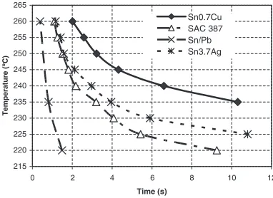
Wettability evaluation under dynamic conditions can be measured with the wetting balance testing, which involves investigation of both wetting times and wetting forces.1)A typical wetting curve is shown in Fig. 1. Commonly measured wetting balance characteristics are the initial wetting time tw, the time for the wetting curve to re-cross the buoyancy force linetb, the maximum wetting force Fmax and the time required to rich the 2/3 of the maximum force
t2=3. The wetting curve comparison for Sn–Pb and three
lead-free alloys, Sn–0.7Cu, Sn–3.5Ag, and Sn–3.8Ag–0.7Cu (SAC387), on cupper substrate is shown in Figs. 2 (235C)
and 3 (260C). Figure 4 shows the measurement results for
initial wetting time at different testing temperatures for all these alloys. Measurements were taken using12:525:0 0:5mm copper test coupons. It can be clearly seen that the wetting times tw, tb and t2=3 for the Sn–Pb alloy are
significantly shorter than those for the lead-free alloys. The best wetting performance for the tested lead-free alloys is from the Sn–3.8Ag–0.7Cu alloy. Increasing the test temper-ature up to 260C decreases the wetting times significantly
for these alloys, Fig. 3. The buoyancy time tb of Sn–3.5Ag and SAC387 alloys is equal to that of the Sn–Pb alloy at higher temperatures (>250C). However, the wetting timetb of the Sn–0.7Cu alloy is still significantly longer as compared
with Sn–Pb eutectic, Sn–3.5Ag and SAC387 at temperatures above 250C. From these wetting balance test results, it is
clear that the lead-free soldering process requires an increase in the process temperature up to 245–250C for Sn–3.5Ag
and Sn–3.8Ag–0.7Cu alloys, and up to 260C for the Sn–
0.7Cu alloy, which has been a candidate lead-free alloy for wave soldering.
Classic wetting theory has been established on simple systems like water or oil on a non-reaction surface, such as glass, at relatively low temperatures. The physico-absorp-tion-dominated wetting driving force is the capillary reaction to reduce the total surface energy in the liquid–solid–vapor system of interest. The restraining force for the wetting or
-30 -20 -10 0 10 20 30
0 2 4 6 8 10
Time (s)
Force (mN)
F 2/3 max
Buoyancy force
tw
tb
t2/3
F
Fig. 1 Wetting balance test interpretation.
-30 -20 -10 0 10 20 30
0 2 4 6 8 10 12 14
Time (s) Force (mN) Sn/Pb Sn0.7Cu Sn3.7Ag SAC 387 Buoyancy force
Fig. 2 Wetting balance curves for Sn–Pb eutectic and lead-free solders at 235C.
-30 -20 -10 0 10 20 30
0 2 4 6
Time (s) Force, (mN) Sn/Pb Sn0.7Cu Sn3.7Ag SAC387 Buoyaoncy Force
Fig. 3 Comparison of wetting curves at 260C for Sn–Pb eutectic and
lead-free solders. 215 220 225 230 235 240 245 250 255 260 265
0 2 4 6 8 10 12
Time (s) Temperature ( ° C) Sn0.7Cu SAC 387 Sn/Pb Sn3.7Ag
[image:2.595.326.525.255.380.2] [image:2.595.329.525.432.564.2] [image:2.595.330.521.619.758.2] [image:2.595.75.266.651.767.2]spreading is viscosity. At balance, the three surface tensions between the liquid/solid substrate (LS), the liquid/vapor (LV), and the solid substrate/vapor (SV), together determine the final wetting angle, which can be expressed as follows:
cos¼SVLS
LV
ð1Þ
Perfect wetting means that the wetting angle approaches zero. For physical wetting, the efficient way to decrease the wetting angle is to increase the surface energy of solid substrate/vapor (SV) by cleaning the solid surface with removal of absorbed species which tend to reduce the surface energy of the solid surface. The surface energy between the liquid/solid substrate (LS), is constant for a given non-reactive solid–liquid system, but very much temperature dependent. As temperature rises,LSdecreases rapidly, thus promoting wetting and spreading of the liquid phase. Small wetting angle indicates a greater spreading, and thus a higher maximum wetting balance force.
The pure physical wetting phenomenon takes place rather quickly (from 100 ns to 10 ms), while wetting or spreading of molten solder takes a much longer time (usually from 0.5 s to up to a few of minutes) as shown in Figs. 2 and 3. This indicates the spreading rate and wetting angle in the soldering process are very much dependent on the complex local metallurgical and chemical reaction kinetics and thermody-namics, not a purely physical wetting process.
The surface tension energies between the liquid/solid substrate (LS) in a solderable system may be significantly different before and after interfacial reactions. The formation of an intermetallic layer reduces the total energy balance at the liquid–solid interface. Assuming the Gibbs free energy per unit area for forming an intermetallic layer between the molten solder and the metallic substrate isGr (which is a negative number), the surface energy between the liquid/ solid substrate can be expressed as:
LS¼LS0 þGr ð2Þ
where0
LS is the surface tension energy between liquid and solid before any interfacial reaction takes place. SinceGris a negative number, the liquid/solid surface tension energy
LS is reduced by the formation of the intermetallic layer, thus reducing the wetting angle according to eq. (1). Furthermore, it has been found that the absolute Gr value is much larger (by two orders of magnitude) than the initial surface energy for molten solders between the liquid/solid substrate, as reported by Yost and Roming2)and Wang and Conrad.3) Therefore, it is clear that anything that affects proper intermetallic formation will cause significant change to the wetting rate and wetting angle, thus the wetting time and maximum wetting balance force.
3.1.2 PCB metallization finishes and aging effects
As stated above, the wetting of a molten solder on metallic surfaces is a rather complex phenomenon. Factors, such as the conditions of the metallic surfaces (i.e., the nature of oxides or other films, surface roughness), temperature distribution during the soldering, as well as the interfacial metallurgical and flux chemical reaction with the metallic surface, all play important roles in determining the final solder wetting and spreading. The soldering process almost
invariably involves many physical-chemical reactions at the interfacial and liquid–solid–vapor junction area. The surface tension energies between the liquid/solid substrate (LS) and between the solid/vapor substrate (SV) are changed rapidly by metallurgical (intermetallic formation) and flux chemical reactions with PCB metallization finishes and/or metallic substrates.
There are many commercially available PCB soldering metallic finishes for lead-free soldering, such as lead-free HASL, using lead-free alloys (such as Sn–Cu, Sn–Ag, or Sn– Ag–Cu alloys) in place of Sn–Pb, electroless nickel and immersion gold (ENIG), immersion Ag and Tin, as well as organic solderability preservative (OSP).4–7) Since metallic finishes or OSP change the chemical affinity with molten solders, the wetting behavior can be significantly different.
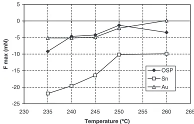
For lead-free soldering, immersion Ni/Au surface finish provides the best wetting results on fresh boards, followed by immersion Sn and OSP, see Fig. 5. However, in a humid condition, the wetting of the immersion Sn finish degrades the fastest, whereas the wetting of the Ni/Au remains excellent as evidenced in Figs. 5 to 6, which show the relative maximum wetting force on 1 inch by 0.5 inch wetting PCB coupons with Sn, OSP and Ni/Au finishes before and after a one-week ageing at 85C/85%RH. The Ni/Au finish
[image:3.595.330.523.457.577.2]remains excellent with variety of pre-conditioning treatments and heat exposures, while OSP loses wettability rapidly with exposure to a high temperature environment, as shown in Fig. 7. Un-aged Ni/Au boards can withstand up to four lead-free reflow cycles before the final reflow soldering process, and at least two reflow cycles before wave soldering process.
-12 -10 -8 -6 -4 -2 0
230 235 240 245 250 255 260 265
Temperature (°C)
Fmax (mN)
OSP Sn Ni/Au
Fig. 5 Relative maximum wetting balance force for virgin coupons with OSP, Sn and Ni/Au finishes (coupons size 1 inch by 0.5 inch).
-25 -20 -15 -10 -5 0 5
230 235 240 245 250 255 260 265
Temperature (°C)
F max (mN) OSP
Sn Au
[image:3.595.328.522.632.756.2]On the other hand, neither fresh nor aged immersion Sn finished boards can withstand multiple lead-free reflow cycles or a reflow cycle prior to wave soldering process without significant degradation in wettability.
3.2 Interfacial intermetallic formation and growth at
liquid–solid interfaces
3.2.1 Intermetallic growth kinetics on Cu substrate
(1) Intermetallic thickness measurement
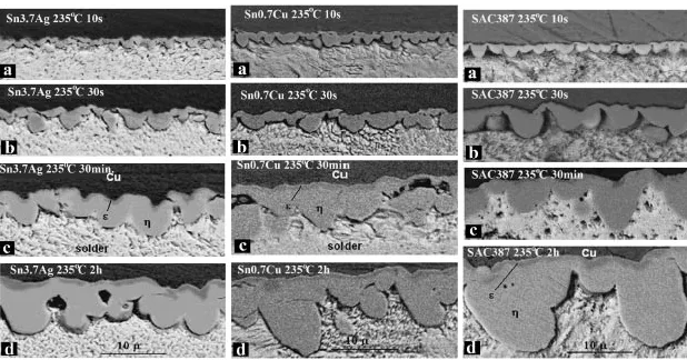
Interfacial reactions between the copper substrate and the three molten lead-free solders, Sn–3.5Ag, Sn–0.9Cu, and Sn– 3.8Ag–0.7Cu, produced a bilayer of Cu6Sn5 adjacent to the
solder and Cu3Sn adjacent to the copper.8)Figure 8 presents
SEM images of IMC layers formed at 235C for 10 s, 3 min, 30 min and 2 h holding times for these three solders. After holding for 10 s, thin Cu6Sn5intermetallic layers of average
thicknesses of 1.18, 1.33 and 1.24mm, were observed respectively for the three alloys. The presence of the Cu3Sn
phase for these samples was not detected at this temperature for such a short time. Cu3Sn phase, however, appears with
[image:4.595.311.541.355.542.2]increased holding time. The final average thicknesses of the IMCs after holding for 2 h were 6.97, 7.65 and 9.44mmfor the three solders on cupper substrate. The maximum thicknesses for the three alloys were determined to be 8.42, 10.37 and 16.5mm. The similarity of the scalloped interme-tallic microstructures for all three alloys indicates that the mechanism of growth is the same for all three. It is clear from
Fig. 8 that the intermetallic grows faster in the Sn–Ag–Cu (SAC387) alloy than in the other two alloys.
Figure 9 illustrates effects of temperature on IMC growth for Sn–3.5Ag alloy at 225 and 280C. The sample held for
30 s does not show the presence of Cu3Sn at 225C.
Increasing the temperature up to 280C promotes Cu 3Sn
layer formation with a thickness of 0.36mm. The total average thickness of the IMC increases by 89% from 1.14mm
up to 2.16mmwith an increase in temperature from 225 to 280C for 2 h holding time.
The IMC layer growth varies depending on the diffusion rates of Cu and Sn through the Cu6Sn5and Cu3Sn layers and
the reactions at the layer interfaces. It is further complicated by the fact that the Cu6Sn5layer is scalloped.9,10)As such, the
thickening or growth kinetics of the total IMC layer has been evaluated by simply assuming parabolic growth. That is, it is assumed that the total layer thickness is given by
w¼w0þkt
1
2 ð3Þ
wherewis the intermetallic layer thickness,tis the holding time,kis the IMC growth rate constant, andw0is the initial
thickness of the IMC layer formed on immersion of the
-14 -12 -10 -8 -6 -4 -2 0
230 235 240 245 250 255 260 265
Temperature (°C)
F max ( mN)
OSP Sn Au
Fig. 7 Relative maximum wetting balance force for coupons after ageing at 130C for 24 h.
Fig. 8 Comparison of SEM images of the intermetallic layers for three lead-free solders: SnAg (left), SnCu (middle) and SnAgCu (right), at 235C and held for 10 s (a), 3 min (b), 30 min (c), 2 h (d).
Fig. 9 The IMC thickness comparison for the SnAg alloy cast at 225C
[image:4.595.74.264.422.542.2] [image:4.595.142.451.595.757.2]copper sample in the solder bath. As such, the measured average layer thicknesses are plotted as a function of the square root of holding time for each temperature studied and fitted with a linear least squares curve to determine the values of k and w0 for each temperature. The k values are
subsequently analyzed to determine the apparent activation energy (Q) for IMC growth using the Arrhenius equation,
k¼k0e
Q
RT ð4Þ
where k0 is the proportionality constant, Q is the apparent
activation energy for IMC layer growth,Ris the Boltzmann constant, and T is the absolute temperature. The apparent activation energyQwas obtained from plots oflnðkÞversus
1=T.
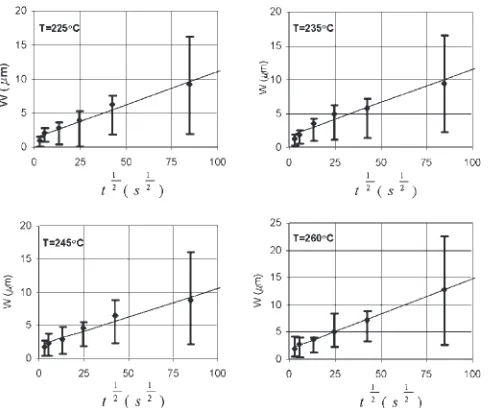
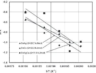
Figure 10 shows the experimental data for IMC layer growth for the SnAgCu (SAC387) alloy as a function of the square root of the holding time for four different temper-atures. The upper and lower limits of the error bars for the thickness measurements for each time represents the thick-ness of the biggest scallop and the deepest cusp between scallops, respectively. As can be seen, the minimum and maximum IMC thickness can deviate up to75% from the average IMC thickness values calculated from the integration of IMC areas. This difference in IMC thickness can clearly be seen in the SEM images (Figs. 8–9).
Comparison of IMC growth for the SnAg (Sn–3.5Ag), SnCu (Sn–0.9Cu) and SnAgCu (SAC387) lead-free solder alloys at five different temperatures are presented in Fig. 11. IMC growth rate constants for the SnAg and SnCu solder alloys are very similar for all test temperatures, while those for the SnAgCu alloy are about 30% greater. This is consistent with the growth rates being greater for the SnAgCu alloy. Comparisons of intermetallic growth for the SnAg, SnCu and SnAgCu alloys at different temperatures are presented in Fig. 12. As can be seen in Fig. 12, the IMC for the SnAg alloy is thinner than that for the SnAgCu alloy for all exposures. This may result from the SnAgCu alloy being
closer to copper saturation at the start of intermetallic growth. It has previously been shown that Cu6Sn5/Cu3Sn
interme-tallic layer growth for eutectic SnPb solders on copper substrates is slower for growth into solder initially containing no copper than for growth into solder initially saturated with copper. Based on previous studies of copper dissolution into molten eutectic SnAg solder, it is expected that saturation of the copper free solder in this study should require about 60 min saturating at 225C.10)
As can be seen in Fig. 12 with soldering at 235C the IMC
layers for the SnAgCu alloy again grows faster than the IMC layer for the SnAg alloy. Further, the SnCu alloy, which is molten at this temperature, grows IMC at about the same rate as the SnAg alloy. Figure 12(b) show a continuation of this trend at 260C, with the difference between the IMC growth
rates for the SnAgCu solders and the SnAg and SnCu solders being the smallest at 280C. One reason for this latter effect
[image:5.595.49.293.70.274.2]may be that, as the temperature increases, the solubility of copper in the molten solders increases. Thus, the presence of copper in the SnAgCu alloy is further from the saturation level and IMC growth in all of the solders is characteristic of growth into a solder with relatively low copper content. Following this reasoning, the IMC growth rates for all three Fig. 10 IMC thicknesswas function of the square root of timetfor the
SnAgCu solder at 225, 235, 245, and 260C. The straight lines represent
mean least square fits of the data.
a)
b)
[image:5.595.330.524.71.434.2]c)
solders studied should approach each other as the soldering temperature increases. Arrhenius plots of the IMC growth are presented in Fig. 13 with apparent activation energies between 22 to 32 KJ/Mole. The values for the SnAg and SnCu alloys are consistent with those reported previously for IMC layer growth for eutectic Sn–Ag solder.11,12)
(2) Initial stage of intermetallic growth on Cu substrate As shown above, some IMC thickness values, notably those for short and long holding times, deviate from the least square fitted average growth line. The deviations are indeed the greatest on a percentage basis at short and long times and they are the greatest for the lower temperatures. The deviation at short times is probably the result of several factors. During the early stage of IMC formation, the IMC
layer is in most cases growing into solder not saturated with copper. Also, the early stage of layer formation may be reaction controlled instead of diffusion controlled. Diffusion models13) of steady state intermetallic growth of Cu6Sn5
between Cu and pure Sn and Sn containing solders also predict power law dependency rather than parabolic depend-ency.
The thickness (w) can also be fit by regression analysis with an equation of the form,
w¼ktnðTÞ ð5Þ
wherekandnðTÞare constants resulting from the fits.nðTÞis found to be from 0.25 to 0.32. The values are consistent with those predicted by diffusion models.14,15) Figure 14 shows calculated best fit curves based on both eqs. (3) and (5) for IMC growth for the SnAgCu alloy at 225C. As can be seen,
the parabolic (n¼0:5) curve fits the data best at time interval of 30 s up to 2 h, while the power law equation works best for short times below 30 s and again at longer times. Similar results were observed at other temperatures for the SnAg and SnCu alloys.
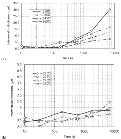
3.2.2 Intermetallic growth on Nickel and Alloy 42
substrates
Unlike extensive study on intermetallic growth of lead-free solders on Cu substrate, there is relatively littlie study on other substrates. SEM images of the intermetallic layers for the Nickel and Alloy 42 (Fe–42Ni) are presented in Fig. 15. It can be seen that intermetallic thickness of Alloy 42 samples is significantly thinner compared with those on both copper and nickel substrates. The comparison of the intermetallic thickness as function of time at different temperatures is presented in Fig. 16. Kinetic parameters of the intermetallic formation were calculated for the Nickel substrate. The value of parameternðTÞin eq. (5) for temperature interval of 225 to
(a)
[image:6.595.71.265.70.374.2](b)
Fig. 12 IMC thickness as function of the square root time for 235C
(a) and 260C (b). Solid lines represent a calculated fit through the
experimental data.
Fig. 13 Arrhenius plot of IMC growth constants (k).
a)
0.0 5.0 10.0 15.0 20.0 25.0
0 10000 20000 30000 40000 50000 60000 70000
t (s)
W (
µ
m)
Experimental data
calculated using Equation 3
calculated using Equation 5
b)
0.0 1.0 2.0 3.0 4.0 5.0 6.0
0 200 400 600 800 1000
t (s)
W (
µ
m)
Experimental data
calculated using Equation 3
[image:6.595.327.522.72.311.2]calculated using Equation 5
Fig. 14 Comparison of two calculated lines (w¼woþkt0:5andw¼ktn)
with experimental data for IMC growth for the SnAgCu alloy at 225C.
[image:6.595.74.263.437.580.2]260C is about 0.475. The calculated activation energyQfor
IMC growth for SAC387 alloy on the Nickel substrate is equal to 86 kJ/mol, which is much higher than with copper substrates. Due to the large scattering for thin intermetallic layer measurement on the Alloy 42 substrate, statistically meaningful growth kinetic equation is not available.
Sn–Ni binary systems have three stable intermetallic compounds, Ni3Sn (at Ni-rich side), Ni3Sn4(at Sn-rich side),
and Ni3Sn2 in the between.16)The additions of Ag and Cu
further complicate the metallurgy at the interface for Sn–Ag– Cu solder alloys. EDAX analysis for the IMC in SAC387 on
the Ni substrate indicates a phase composition close to (NiCu)3Sn4 compound. No Ni-rich IMC was detected in the
samples tested.
For Alloy 42 substrate, the alloy itself is a mixture of-Fe plus Fe3Ni compound. Since atomic Ni is not available, the
intermetallic phase at the interface of SAC387 and Alloy 42 would be mainly Sn–Fe intermetallic compounds. The Fe–Sn binary system has two stable intermetallic phases: FeSn at the Fe-rich side and FeSn2 at the SN-rich side. The EDAX
analysis shows a FeSn2 intermetallic compound is the
[image:7.595.49.290.70.318.2]predominant IMC for SAC387 on Alloy 42 substrate. Figure 17 presents the growth behavior of the IMC layers formed between molten SnAgCu solder and Ni, Cu, and Fe– 42Ni substrates at 260C. It is clear that the (Cu,Ni)6Sn5
forming between Ni substrate and the solder grows the fastest. This is not surprising considering the different mechanisms involved in their formation.
3.2.3 Orientation imaging microscopy analysis on
in-termetallic compounds
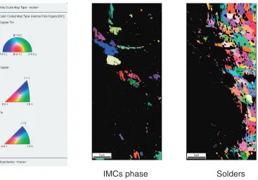
OIM is a methodology that uses electron backscatter diffraction (EBSD) patterns data to analyze crystallographic orientations and phase identification. Once the backscattered electron diffraction data is collected, OIM analysis is then conducted for analyzing orientation and related aspects of crystalline microstructures, such as orientation distributions of the grain microstructure or orientation relationship between two different phases. It is found from this study that IMC (mostly Cu6Sn5) exists not only in the interface
region, but also in the solder matrix at early stage of IMC growth (see Fig. 18), indicating intermetallic growth and dissolution take place at the same time. The IMC was identified with a hexagonal structure. An attempt was also made to gain information on the orientation relationships. The interface as well as solder matrix and Cu substrates were scanned and mapped with OIM (see the color coded orientation maps in Fig. 19). The technique shows if any definitive preferred orientation relationship exists between the IMC phase and the Cu substrates or solders. For the sample examined (3 min at 280 C), it is clear from the IOM scans that the IMC scatters cross a wide—range interfacial area than the measured IMC thickness. However, conclusive orientation preferences of IMCs with respect to substrate and solder will require detailed analysis of many more samples, which is still in progress at the time of this publication. Fig. 15 Comparison of SEM images of the intermetallic layers for the Ni
samples cast at 235C (a–e) and 245C (f–j) held for 10 s, 3 min, 10 min,
and 2 h.
(a)
(b)
Fig. 16 Thickness of intermetallic as function of time for SAC387 on (a) Nickel, (b) Alloy 42.
0 5 10 15 20 25 30 35
0 2000 4000 6000 8000
Time (s)
W (
µ
m)
[image:7.595.333.523.74.196.2]Cu Ni Alloy 42
Fig. 17 Comparison of the plots of intermetallic (IMC) layer thickness (w)
[image:7.595.70.268.378.605.2]4. Conclusions
The study of wettability and intermetallic growth kinetics for three lead-free solders: Sn–Ag eutectic (96.5%Sn– 3.5%Ag), Sn–Cu eutectic (99.3%Sn–0.7%Cu) and Sn–Ag– Cu eutectic (Sn–3.8Ag–0.7Cu, SAC 387), illustrated signifi-cantly different characteristics on different PCBs with OSP, immersion Sn, and Ni/Au finishes, and with metallic substrate Cu, Ni, and Alloy 42 (42%Ni–52%Fe):
(1) The wetting timetband wetting force of Sn–3.5Ag and SAC387 approach to those of Sn–Pb eutectic at temperatures above 250C on Cu substrate. Sn–0.7Cu
alloy, which has been a candidate lead-free alloy for wave soldering, shows a lagging wetting performance even above 250C.
(2) Among Ni/Au, Sn and OSP finishes, Ni/Au maintains its good wettability after exposure to humidity and high
temperature, while humidity degrades wettability sig-nificantly for immersion Sn finish, and OSP loses wettability rapidly with exposure to a high temperature environment.
(3) Morphologically, the formation and growth of IMC layers between all three lead-free alloys and copper substrate are identical, with formation of a thin layer of Cu3Sn adjacent to the copper substrate and a scalloped
layer of Cu6Sn5between Cu3Sn and the molten solders.
[image:8.595.113.484.74.251.2](4) The IMC layer formed with the SnAgCu alloy grows faster than those formed with the SnAg and SnCu alloys on Cu substrates. The faster growth of the IMC layers for the SnAgCu alloy may be the result of the layers growing into a solder initially containing more copper for the SnAgCu alloy. Among Cu, Ni and Alloy 42 metallic substrates, Cu grow intermetallic layers fastest, followed by Ni, and Alloy 42 at lower temperatures, Fig. 18 Electron backscatter diffraction (EBSD) patterns on sample 280C, 3 min. Indicating IMC in the matrix (area marketed).
IMCs phase
Solders
[image:8.595.117.484.289.546.2]while at higher temperatures (above 260C) Ni grows intermetallic faster than Cu and Alloy 42 due to a much higher activation energy for Ni intermetallic growth kinetics.
REFERENCES
1) ANSI/J-STD-003, ‘‘Solderability Tests for Printed Boards’’, (1992). 2) F. G. Yost and A. D. Romig: Mater. Res. Soc. Symp. Proc.108(1988)
385–390.
3) H. Wang and H. Conrad: Metall. Mater. Trans.26A(1995) 495–469. 4) R. Gordon, S. Marr and D. Shangguan: Proceedings of SMTA
International Conference, Chicago, September (2000) pp. 583–591. 5) M. Arra, D. Shangguan and D. Xie: Proceedings of APEX 2003,
Anaheim, CA (2003) pp. S209-2-1/5.
6) M. Arra, D. Shangguan, J. Sundelin, T. Lepisto¨ and E. Ristolainen:
Proceedings of the 3rd IPC/JEDEC Annual Conference on Lead-Free Electronic Assemblies and Components, (2003) pp. 170–179.
7) M. Arra, D. Shangguan, D. Xie, J. Sundelin, T. Lepisto¨ and E. Ristolainen: Proceedings of Soldertec/IPC International Lead-free Conference, Brussels, Belgium (2003) pp. 423–446.
8) N. Dariavach, P. Callahan1, J. Liang and R. Fournelle: to be published inJ. Electron. Mater.34(2005).
9) K. Suganuma and G. Nakamura: J. Jpn. Inst. Met.C59(1995) 1299. 10) M. Schaefer, W. Laub, R. A. Fournelle and J. Liang: Design and
Reliability of Solders and Solder Interconnects, ed. by R. K. Mahidhara
et al.(Warrendale, PA: TMS, 1997) pp. 247.
11) S. Chada, R. A. Fournelle, W. Laub and D. Shangguan: J. Electron. Mater.29(2000) 1214.
12) S. Chada, W. Laub, R. A. Fournelle and D. Shangguan: J. Electron. Mater.28(1999) 1194.
13) H. K. Kim and K. N. Tu: Phys. Rev. B53(1996) 16027.
14) M. Schaefer, R. A. Fournelle and J. Liang: J. Electron. Mater.27(1998) 1167.
15) R. A. Gagliano and M. E. Fine: J. Electron. Mater.32(2003) 1441. 16) ASM Handbook, Vol. 8 Metallography, Structures and Phase Diagrams,