Self-Correcting Power Generation in
mm-Wave Circuits and Systems
Thesis by
Steven M. Bowers
In Partial Fulfillment of the Requirements
for the Degree of
Doctor of Philosophy
California Institute of Technology
Pasadena, California
2014
Acknowledgments
“Success is not a random act. It arises out of a predictable and powerful set of circumstances and opportunities.”
-Malcolm Gladwell
This is a quote from one of my favorite books,Outliers: The Story of Success, by Malcolm Gladwell. The basic theme of the book is that great things are done by intelligent people who are presented with great opportunities. To be sure, people need to take those opportunities, but in almost all cases, there are great people supporting those that end up getting the credit. I believe that often success stories are as much about the people achieving success as about those that support them, and in educational success stories, it is the teachers who may not always get the credit they deserve. For me personally, the multitude of teachers in my life have shaped my intellect, my ideologies and my personality, and I am grateful for everything they have done for me. I have worked hard to achieve what I have, but an equal amount of credit goes out to those that gave me the opportunity to do something great. There are more of them than I can possibly hope to thank personally here, but I hope to acknowledge those that had the greatest impact on my life in the paragraphs to follow.
It may seem trite, but the person who had the single biggest contribution to my personal ideologies, what I consider to be the core of who I am, outside of my immediate family was my kindergarten teacher Mrs. Munemo. She taught me the value of true empathy; taking a moment to stop and consider exactly what it might be like to be in the position of someone else. This ability to empathize with those I disagree with has been invaluable to me on many occasions, and has enabled me to identify mistakes in judgement I have made early, and to appreciate all of the opportunities that I have been lucky enough to receive. She may have given me an unsatisfactory mark in skipping (I have practiced, and truly excel at skipping now), but I remember her for her firm insistence that if a judgement that is to be made about a person, it must be based upon their merits and not the circumstances of their upbringing, cultural background, or socioeconomic status.
normal course of whatever the experiment was, would ask what else I could do with the components from the kit. If there was a beginning to my research career, this was it. They helped foster a curiosity that would not accept any answer “because that’s the way it is,” but rather required a logical explanation for anything in my world that didn’t fit the reality my mind expected. There were many other teachers and mentors in my personal life growing up, but I would like to personally thank: Ann Blanton and Gary Maxwell, Colleen Kegg and Bob Simon, Karen Kegg and Tim Johnson, and my best friends in grade school, Andrew Maxwell, Jeff Simon, and Andy Johnson.
Since I was little, I knew I wanted to be an electrical engineer like my Dad (more on that later), but I first knew I wanted to be a teacher my junior year in High School in my AP physics class with Mr. Abo-Shaer. It was his first year at Dos Pueblos High School, and I have never seen such a passion for teaching others before or since then. We had the usual discussion about the curriculum of the class, but I will remember him most for our discussions about the way he taught the first year physics course. AP physics was the first class I took where the teacher also taught a lower level class. Being in the AP class, I was able to discuss with Mr. Abo-Shaer the challenges of being a first-year teacher, and teaching the lower-level class for the first time. It was the first time that I was able to see the impact that a teacher could have on his students from the perspective of someone who had already taken the class. A great teacher will always find a way of showing their students their full potential, and motivating them to achieve it, rather than focusing on their shortcomings and failures.
Between my junior and senior year of High School, I had the privilege of being part of the apprentice researcher’s program at UCSB run by Wendy Ibson, a program where local high school students worked with graduate students on cutting edge research. I worked in the Physics Department on onset voltages of chaotic patterns in nematic liquid crystals. Wendy provided the necessary glue that enabled the inexperienced high school students to interact with the generous graduate students. I had the opportunity to present my research at the 2002 Southern California Conference for Undergraduate Research at Caltech, so in the end the program introduced me to three things: academic research, conference publications and presentations, and Caltech, which years later would become my home.
convinced me that pursuing a Ph.D. in graduate school was the path I wanted to pursue. One might take notice that the first two of my undergraduate mentors are in the field of photonics, but my graduate research has mainly focused on mm-wave circuit design. While I loved the work I was doing in photonics, a microwave circuit class I took with Dr. Rebeiz my junior year at UCSD peaked my interest, and changed my research trajectory. Dr. Rebeiz cared passionately for his students, and would always make time for those interested to ask questions or learn about subjects from the class or from his group’s research.
After college I started my graduate studies at Caltech, and was fortunate enough to step into a lab with an amazing group of students. My sincerest gratitude goes out to all of the students of the CHIC and MICS lab including Aydin, Yu-Jiu, Hua, Ed, Jay, Jenny, Joe, Amir, Alex, Behrooz, Firooz, Costis, Matt, Meisam, Manuel, Saman, Mayank, and Krishna, who early on helped me get up to speed on the state of the art in IC design, and later on who helped me reach deadlines that often seemed impossible. I need to thank both Kaushik (K1) and Kaushik (K2) for always being willing to grab a cup of coffee on the balcony, and Juhwan and Florian for always having words of encouragement if research wasn’t going quite as planned. I was also lucky enough to work with both Kaushiks, Amir, Alex, Behrooz and Firooz as collaborators on parts of the research presented in this thesis, and thank them for all the long hours we put in to get results. I was able to TA for Dr. Behnam Analui when he was a guest lecturer at Caltech, and learned a great deal from our discussions about lecturing at the college and graduate levels.
When I first was talking to my advisor, Prof. Ali Hajimiri, about coming to Caltech, and also deciding about pursuing microwave circuits verses optical electronics, I remember asking what I was worried would be a dangerous question. There is a large amount of iterative work being done in circuits, where increased performance is gained by redesigning an old well-known architecture in a new advance process. I asked Ali if he thought there was still room for truly innovative circuit design, and after some careful consideration, he replied that he had no interest in iterative designs, and that in order to succeed in the group, novel designs were going to be critical. He would be willing to take on the risks of a student learning an entirely new area of research that the group was not an expert on in order to produce truly innovative work, but had no time for porting old designs to new processes. This is a mentality that I really agree with, though it is also very risky. In a field where world-record performance specifications are what get noticed (sometimes even above innovative design), passing up a sure thing that is less interesting to swing for the fences on new designs can backfire, but graduate school is exactly the time to take large risks, especially in your research, and to strive to achieve lasting contributions to the field. I also owe a large debt of gratitude to him for giving me the freedom to pursue the path of research that interested me the most, and to allow me to take projects I was working on in new and interesting directions, rather than sticking to a prearranged project plan set out early on.
Weinreb’s passion for research is inspiring, and his measurement expertise has been beneficial on several occasions. I thank Prof. Choo for his friendly encouragement and advice, and Prof. Vahala for his invaluable discussions as I took on a new field of research in silicon photonics toward the end of my studies. I would also like to thank Prof. Volnei Pedroni, who has always showed great interest and enthusiasm in my research. A portion of this work was done as part of a project with IBM T.J. Watson laboratory, and I want to thank everyone there that we worked with, including Jos´e Tierno, Dan Friedman, Ben Parker, and Herschel Ainspain for their efforts throughout the project.
There are a great many people who are required to keep a research lab operating, many of whom likely don’t get nearly the credit they deserve, but many many thanks go out to everyone who enabled me to do the research presented in this thesis, including Carol, Tanya, Estella and Michelle. I think that our lab would have imploded several times over in the time I have been there if not for Michelle’s efforts to keep everything up and running.
Finally, I need to thank my family for all the support they have given me, which has always been unwa-vering. I am incredibly fortunate to have grown up with two excellent role models as my parents. They’ve always done the perfect job of striking the balance of encouraging me to succeed while letting me learn and even fail on my own. My Dad stoked my interest in technology at a young age. We always were building something, whether it was a train set, or a robotics kit or a go kart or a club house. Building things was some-thing that I took somewhat for granted, as it had always been a part of my life, but after coming to Caltech, I have realized what a valuable skill set it is to be able to look at an object, figure out its functionality, and if broken, be able to fix it. My Dad is an engineer, and from early on I knew that I wanted to be one as well. Now that I have seen the inner workings of academia, I marvel that he was able to spend so much time with us as kids, but I am incredibly grateful for every moment of it. More than anything else though, I am grateful that he has taught me what it means to be a great father, and I hope to do at least half as good a job in that role as he did for me.
and my late Grandpa Durbahn also deserve thanks for helping me grow and mature as a person. Though not strictly family by blood, Jason Wiese has been like a brother to me since college, and his support has been instrumental to my ability to complete this degree, and for that I am grateful.
My wife Christine has kept me sane throughout my studies at Caltech. If there is anyone who truly knows the hours that were put in to produce this work it is her. There were endless long nights, early mornings, and weekend plans that were canceled to meet the dreaded tapeout deadlines, and yet she was always there supporting me regardless of the hour of the night or the wrenches I threw into her plans. One of my single lab mates once asked me how I could still get all my work done while being married, and to this day I wonder how any of them can get all of their work done without the support I have gotten every night when I come home. Her understanding seems to know no bounds, though I always seem to find ways of pushing it further. She has taught me that it is ok to fail, if you learn from that failure and use that knowledge to help you succeed in the future. She is now carrying our first child, and I cannot think of anyone I would rather be the mother of my children than her.
There are many more people who have enabled me to succeed in this endeavor, and though there is not room to thank every one of them individually, I am deeply thankful to everyone who has helped me along the way.
Abstract
This thesis presents novel design methodologies for integrated radiators and power generation at mm-wave frequencies that are enabled by the continued integration of various electronic and electromagnetic (EM) structures onto the same substrate. Beginning with the observation that transistors and their connections to EM radiating structures on an integrated substrate are essentially free, the concept of multi-port driven (MPD) radiators is introduced, which opens a vast design space that has been generally ignored due to the cost structure associated with discrete components that favors fewer transistors connected to antennas through a single port.
From Maxwell’s equations, a new antenna architecture, the radial MPD antennas based on the concept of MPD radiators, is analyzed to gain intuition as to the important design parameters that explain the wide-band nature of the antenna itself. The radiator is then designed and implemented at 160 GHz in a 0.13µm SiGe BiCMOS process, and the single element design has a measured effective isotropic radiated power (EIRP) of +4.6 dBm with a total radiated power of 0.63 mW.
Next, the radial MPD radiator is adapted to enable dynamic polarization control (DPC). A DPC antenna is capable of controlling its radiated polarization dynamically, and entirely electronically, with no mechani-cal reconfiguration required. This can be done by having multiple antennas with different polarizations, or within a single antenna that has multiple drive points, as in the case of the MPD radiator with DPC. This radiator changes its polarization by adjusting the relative phase and amplitude of its multiple ports to produce polarizations with any polarization angle, and a wide range of axial ratios. A 2x1 MPD radiator array with DPC at 105 GHz is presented whose measurements show control of the polarization angle throughout the entire 0◦through 180◦range while in the linear polarization mode and maintaining axial ratios above 10 dB in all cases. Control of the axial ratio is also demonstrated with a measured range from 2.4 dB through 14 dB, while maintaining a fixed polarization angle. The radiator itself has a measured maximum EIRP of +7.8 dBm, with a total radiated power of 0.9 mW, and is capable of beam steering.
two-dimensional beam steering. Finally, a third design incorporates multi-antenna DPC by combining the outputs of both left and right handed circularly polarized MPD antennas to produce a linear polarization with controllable polarization angle, and has a simulated gain of 11.9 dBi and EIRP of -3 dBm. In simulation, it can tune the polarization from 0◦ through 180◦ while maintaining a radiated power that has a 0.35 dB maximum deviation from the mean.
The reliability of mm-wave radiators and power amplifiers was also investigated, and two self-healing systems have been proposed. Self-healing is a global feedback method where integrated sensors detect the performance of the circuit after fabrication and report that data to a digital control algorithm. The algorithm then is capable of setting actuators that can control the performance of the mm-wave circuit and counteract any performance degradation that is observed by the sensors. The first system is for a MPD radiator array with a partially integrated self-healing system. The self-healing MPD radiator senses substrate modes through substrate mode pickup sensors and infers the far-field radiated pattern from those sensors. DC current sensors are also included to determine the DC power consumption of the system. Actuators are implemented in the form of phase and amplitude control of the multiple drive points.
Contents
Acknowledgments iv
Abstract ix
1 Introduction 1
1.1 Contributions . . . 2
1.2 Organization . . . 3
2 On-Chip Radiation and Power Generation from mm-Wave Integrated Circuits 5 2.1 Efficient Radiation from an On-Chip Antenna . . . 5
2.2 State of the Art in On-Chip Integrated Radiators . . . 9
2.3 Performance Degradation due to Process and Environmental Variation . . . 12
2.4 Current Technology in Adaptive and Self-Healing Circuits . . . 14
3 Multi-Port Driven Radiators 17 3.1 Introduction . . . 17
3.2 Multi-Port Driven Antenna Architecture and Analysis . . . 19
3.2.1 Broadside, Far-Field Radiation From Currents on a Plane . . . 20
3.2.2 Multi-Port Driven Antenna Architectures . . . 21
3.2.3 Solution to Currents on the Ring . . . 24
3.2.4 Solution to Current on the Spokes . . . 26
3.2.5 Summing up the E-fields From All Ports . . . 28
3.2.6 Summation of Fields of a Multi-Port Driven Antenna . . . 28
3.2.7 Poynting Vector and Effective Isotropic Radiated Power . . . 30
3.3 Design and Simulation of a Multi-Port Driven Antenna . . . 31
3.4 Driver Circuitry of a Multi-Port Driven Radiator . . . 34
3.4.1 Oscillator Design . . . 35
3.4.2 Amplifier Design . . . 37
3.6 Multi-Port Driven Radiator Measurements . . . 41
3.7 Slot-Based Radial Multi-Port Driven Radiator . . . 46
3.7.1 DC Coupled Slot Multi-Port Driven Antenna . . . 48
3.7.2 2x2 AC Coupled Slot Multi-Port Driven Radiator Array . . . 48
3.8 Differential Drive Multi-Port Driven Antennas . . . 52
3.8.1 Virtual Shorts to Lower Input Impedance in Multi-Port Driven Radiators . . . 52
3.8.2 Linear Differential Multi-Port Driven Radiator . . . 53
3.8.3 Passive 2 GHz Differential Multi-Port Driven Test Structure on FR4 PCB . . . 55
3.9 Conclusions . . . 58
4 Dynamic Polarization Control and Modulation 59 4.1 Electromagnetic Polarization . . . 60
4.2 Dynamic Polarization Control . . . 63
4.2.1 Dynamic Polarization Control with Multiple Antennas . . . 63
4.2.2 Dynamic Polarization Control Through a Single Multi-Port Driven Radiator . . . 66
4.3 Proof of Concept of a 2x1 Multi-Port Driven Radiator Array with Dynamic Polarization Control 66 4.3.1 Measurements of the 2x1 Multi-Port Driven Radiator Array . . . 70
4.4 Polarization Modulation . . . 75
4.5 Conclusions . . . 76
5 Optically Generated mm-Wave Power 78 5.1 Integrated Silicon Processes . . . 78
5.1.1 Waveguides . . . 79
5.1.2 Photodiodes . . . 80
5.1.3 Optical Phase Modulators . . . 80
5.1.4 Metal Stack . . . 82
5.2 Producing THz Signals from Two Lasers . . . 83
5.2.1 Radio Frequency Phase Shifting Using Optical Phase Modulators . . . 84
5.3 Optical Multi-Port Driven Radiators on Silicon Photonics Process . . . 85
5.3.1 Measurements from Optical Multi-Port Driven Antennas . . . 92
5.3.2 Improvements for Second Fabrication Run . . . 92
5.4 Conclusion . . . 92
6 Self-Healing of an Integrated Multi-Port Driven Radiator Array 94 6.1 Mode Pickup Sensor Simulations . . . 95
6.1.1 Sensing Changes In Substrate Thickness . . . 96
6.2 Mode Pickup Test Structures in 2x1 Multi-Port Driven Radiators . . . 101
6.3 Self-Healing a 2x2 Radiator Array . . . 104
7 Self-Healing Power Amplifier 107 7.1 Motivation for Self-Healing . . . 107
7.2 Introduction to Self-Healing . . . 108
7.2.1 Self-Healing Blocks . . . 110
7.2.2 Block Level Versus Global Healing . . . 112
7.2.3 Design Considerations and Architecture for an Example Self-Healing Power Amplifier 112 7.3 Actuation: Countering Performance Degradation . . . 115
7.3.1 Gate Bias Actuators . . . 116
7.3.2 Passive Matching Network Tuning Actuators . . . 117
7.3.3 Supply Voltage Actuators . . . 120
7.3.4 Transistor Architecture Actuators . . . 122
7.4 Sensors, Data Converters, and Digital Algorithm . . . 122
7.4.1 Sensors . . . 122
7.4.2 Data Converters . . . 124
7.4.3 Digital Algorithm . . . 124
7.5 System Measurements . . . 127
7.5.1 Self-Healing Measurements with 50ΩLoad . . . 127
7.5.2 Self-Healing Under Load Mismatch . . . 130
7.5.3 Power Amplifier Linearity Measurement . . . 132
7.5.4 Self-Healing Laser-Induced Transistor Failure . . . 132
7.5.5 Yield Improvement and Performance Summary . . . 133
7.6 Conclusion . . . 133
8 Conclusion 138 A Mapping Current on a Plane to Broadside Far-Field Electric Field 140 A.1 General Mapping of Currents to Electric Fields in the Far Field . . . 140
A.2 Solution for Point Sources . . . 142
A.3 Far-Field Approximation . . . 144
A.4 Solving the broadside, far-field radiation from currents on a plane. . . 146
C.2 Capacitance Tuning of Transmission Lines . . . 151 C.3 Tunable Transmission Line Test Structures . . . 152
List of Figures
2.1 Depiction of electromagnetic rays reflecting and refracting within a substrate, and the surface modes excited by a dipole for different substrate thicknesses. . . 6 2.2 Operation of a silicon lens to minimize substrate waves and to radiate the highest power down
through the bottom of the substrate. . . 7 2.3 3-dimensional depiction of the use of a dielectric superstrate (quartz in this case) to couple
electromagnetic power up from the metal stack to antennas printed on top of the superstrate. . 7 2.4 Radiation scheme showing silicon lens, block diagram and die photo. . . 8 2.5 3-dimensional rendering of the patch antenna, and the die photo. . . 8 2.6 Conceptual depiction of a single distributed active radiator (DAR), and the block diagram of
the 4x4 DAR phased array. . . 10 2.7 Block diagram of the transmitter and receiver, and the die photo of the transmitter showing the
radiator array. . . 11 2.8 3-dimensional depiction of the four leaky wave transmission line antennas, their use for both
transmitter and receiver, and a die photo showing the transceiver. . . 11 2.9 Block diagram of the transceiver and die photo showing transmit and receive antennas. . . 12 2.10 (a) Two main sources of variation in a MOSFET, and (b) threshold voltage variation over
technology node. . . 13 2.11 (a) Output power variation with voltage standing wave ratio (VSWR) magnitude for a fixed
phase, and (b) variation with phase variation for a fixed VSWR magnitude for one design of a mm-wave power amplifier (PA). . . 14 2.12 Block diagram of the self-healing synthesizer to suppress spurious tones, and the die photo of
its implementation. . . 15 2.13 Block diagram of the transmitter half of the self-healing system, and the die photo of the entire
self-healing transceiver. . . 15
3.2 Instantaneous current distribution for the traveling current wave around the ring for four phases: (a) 0o, (b) 90o, (c) 180o, and (d) 270o, where the integrated current vector depicted as the
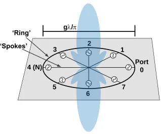
dashed arrow shows maximum currents on ring pointing in the same direction for all phases. . 22 3.3 Proposed MPD antenna architecture showing ring and ground spokes with an overlay of the
expected radiated beam, as well as design variablesgandN. For this design there are 4 spokes soN = 4. . . 23 3.4 (a) Shows the ring portion of the MPD antenna being driven by only ports 0 and N as part of
the overall superposition analysis, while (b) depicts the location of the virtual shorts observed under these driving conditions and (c) shows the counterclockwise oriented standing wave current along the ring, where the sign of the maximum current changes sign betweeng < 1
andg >1at 0 phase for the first two quadrants. . . 24 3.5 (a) Shows the spoke portion of the MPD antenna being driven by only ports 0 andNas part of
the overall superposition analysis, noting that the phase of the current driven into the ground spokes is opposite of that for the ring, and (b) depicts the location of the virtual short circuit observed at the origin and (c) shows the standing wave current along the driven spoke at 0 phase. 27 3.6 Simulated instantaneous current at phase 0 on a ring (a) and spokes (b) driven by ports 0 and
N, wheng= 0.7. . . 31 3.7 Simulated instantaneous current at phase 0 on a ring (a) and spokes (b) driven by ports 0 and
N, wheng= 1.3. . . 32 3.8 MPD antenna with substrate mounted on a PCB ground plane, with traveling wave currents
on the ring marked as solid red arrows, and standing wave ground spoke currents marked with dashed blue arrows, and an overlay of the radiated beam. . . 33 3.9 Simulated radiation pattern of the gain in dBi of the MPD antenna of Figure 3.8 with lossy 10
Ωcm substrate and lossless conductors shows a maximum 4.4 dBi gain. . . 34 3.10 Block diagram of the MPD radiator showing driver circuitry blocks as well as ring of MPD
antenna (ground spokes omitted for clarity). . . 35 3.11 Schematic of the 8-phase ring oscillator that uses AC coupling capacitors to allow a cascode
architecture as well as to create capacitive dividers that enable single stage voltage gains greater than 1 even at steady state. Bias circuitry omitted for clarity. . . 36 3.12 Plot of the power gainGmof a single cascode stage with voltage amplitude gains (A) of 1.0,
2.0 and 5.5, with voltage phase shifts of 45o. At 160 GHz, withA= 2.0,Gm= 16.1mS. . . 36
3.13 3-dimensional rendering of the oscillator inductors implemented as differential transmission lines that have trimmable short circuits that can be cut to enable 3 different frequency bands. . 37 3.14 Schematic of the class A cascode power amplifier stages that each produce -7.0 dBm at 160
3.15 Layout for the driver core feed lines electromagnetic simulation. All 8 feed lines, as well as the 4 differential oscillator inductors and all ground lines were simulated to ensure amplitude and phase matching for the feed lines, and isolation between feed lines and oscillator inductors. 39 3.16 The feed line simulation was coupled with an antenna simulation that included the effects of
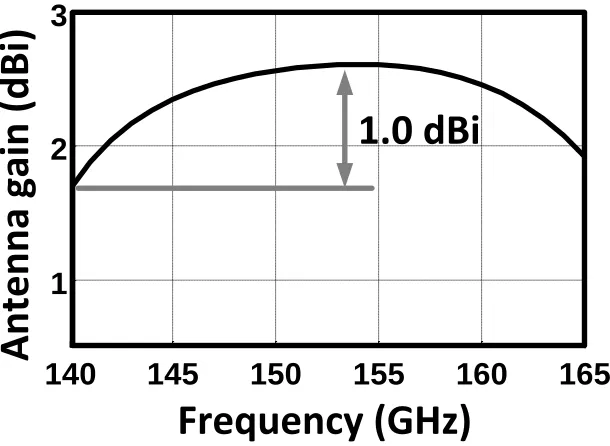
the driver core ground and the PA biasing line (a), with the resulting radiation pattern of the gain in dBi in (b) showing a maximum gain of 2.4 dBi. . . 40 3.17 Simulated gain of the MPD antenna including feed lines from 140 to 165 GHz shows a
max-imum gain deviation of 1 dBi across that band and demonstrates the expected wide band per-formance of the MPD antenna. . . 40 3.18 Photo of the measurement setup with EM dampers removed and the harmonic mixer attached
to the receive antenna (a), and diagram of the measurement setup where received power goes either to a harmonic mixer for frequency measurements or to an Erikson power meter for absolute power measurements (b). . . 42 3.19 Measured spectrum of the single element MPD antenna shows -25.6 dBm captured power at
161.45 GHz which corresponds to 4.6 dBm EIRP. . . 43 3.20 Normalized power captured in dB by a linearly polarized antenna as the chip is rotated in the
X-Y plane. Ratio of maximum to minimum powers of 1.315 imply a polarization ratio of 14.6, which means that the radiation is almost entirely in the CW circular polarization. . . 43 3.21 Simulated and measured radiation patterns of EIRP in dBm in the elevation (a) and azimuth
(b) planes show a single beam radiating broadside to the chip that matches well with simulation. 44 3.22 Measurements from the three frequency bands at 145, 154 and 161 GHz show radiated EIRPs
above 0 dBm for all 3 bands. . . 45 3.23 Die photo of the single element MPD radiator with area of 1 mm2. . . 46 3.24 Comparison between the line version of the MPD radiator (left), and its dual, the slot MPD
radiator (right). Each of the four drive points drive the outer metal plane against the inner metal plane and are phased evenly (0◦,90◦,180◦ and270◦) to create a circularly polarized radiated field. . . 47 3.25 Block diagram of the DC coupled slot radiator, where the outer metal plane is biased at VDD,
and the inner plane is biased at 0 V. . . 48 3.26 Antenna pattern of the DC coupled slot MPD radiator showing a maximum gain of 3 dBi with
downward radiation. . . 49 3.27 Cross section of the tri-level transmission line that maintains an RF open circuit between the
3.29 Radiation pattern of the 2x2 slot MPD array showing downward radiation with a maximum gain of 5.4 dBi . . . 51
3.30 Small loops have currents that cancel in the far field (left). What is needed is a current sink that creates a short circuit without needing to loop back (center). The use of multiple drive points with virtual short circuits between them provides this current sink (right) . . . 53
3.31 Block diagram of the differential linear MPD radiator showing differential drivers that are fed perpendicular to the antenna, and VDD lines that are connected in parallel to the virtual short circuits on the antenna. . . 53
3.32 Simulated current distribution of the differential linear MPD radiator showing instantaneous current all pointed in the same direction, leading to effective radiation. . . 54
3.33 Block diagram of the differential linear MPD radiator showing on chip oscillator, and division and amplification stages is shown on the left. A 3D depiction of the metal structures of the radiator is shown on the right. . . 55
3.34 Simulated antenna pattern of the differential linear MPD radiator shows a maximum gain of 4.5 dBi. . . 55
3.35 Layout of the differential linear MPD radiator in a 65nm bulk CMOS process. . . 56
3.36 Photo of the fabricated passive differential linear MPD antenna scaled to operate at 2 GHz . . 56
3.37 Simulated antenna pattern of the PCB differential linear MPD antenna shows a maximum gain of 5 dBi. . . 57
3.38 Simulated and measured antenna patterns in the elevation (left) and azimuth (right) planes match closely with electromagnetic simulations. . . 57
4.1 Examples of electromagentic polarization, with linear polarization having polarization angle
φ(upper left), elliptical polarization having polarization angle φand axial ratiom/n(upper right), left-hand circular polarization (lower left) and right-hand circular polarization (lower right). . . 61
4.2 2 dipoles in same orientation that are polarization matched and thus have maximum coupling (a), and 2 dipoles that are orthogonal and thus no signal will be picked up by the receive antenna (b). . . 62
4.3 Dynamic Polarization Control (DPC) radiator can switch between various electromagnetic po-larizations to match different receivers regardless of their polarization or spacial orientation. . 63
4.5 The superposition of two linearly polarized fields that are in phase will also result in a linearly polarized field, where the polarization angle is determined by the relative amplitudes of the original two linearly polarized fields. . . 65 4.6 Breaking up the MPD radiator into two using superposition shows how it can be considered as
two linearly polarized radiating elements that are overlapping in space and which are somewhat isolated from each other due to being driven at the axis of symmetry of the other set of drives. This enables the DPC radiator to change its polarization by changing the amplitude and phase of the two radiating subparts. Below each subpart is a depiction of the two current distributions for each subpart showing the nodes on the rings that cause the currents to line up in the same direction and create effective radiation. . . 67 4.7 Block diagram of 2x1 DPC radiator array showing individual radiators, the locking network,
and control of frequency, phase and gain to enable dynamic polarization control. . . 68 4.8 Schematics of Circuits used in the 2x1 DPC radiator array, with the VCO with first amplifier
stage on top, the cascode amplifier used for the second two stages in the lower left, and the phase rotators in the lower right. . . 69 4.9 Simulated antenna pattern of the 2x1 radiator array in linear polarization mode showing a
maximum 1.37 dBi gain. . . 70 4.10 Simulated antenna pattern of the 2x1 radiator array in circular polarization mode showing a
maximum 0.76 dBi gain. . . 71 4.11 Simulated antenna pattern of the 2x1 radiator array with each radiator in an opposite circular
polarization mode to produce a linear polarization, and again showing a maximum 0.76 dBi gain. 71 4.12 Measurement setup for the 2x1 DPC radiator array. . . 72 4.13 Measurements showing a full tuning range from 0◦through 180◦while maintaining axial ratios
above 10 dB the entire time for 3 directions of radiation: broadside, with the beam aimed broadside, 20◦off axis in the axis of the array, with the beam aimed toward the direction of the receiver, and 30◦off axis perpendicular to the the axis of the array, with the beam aimed broadside. . . 72 4.14 Measurements showing control over the axial ratio while maintaining a fixed polarization angle
for 3 directions of radiation: broadside, with the beam aimed broadside, 20◦ off axis in the axis of the array, with the beam aimed toward the direction of the receiver, and 30◦ off axis perpendicular to the the axis of the array, with the beam aimed broadside. . . 73 4.15 Measured antenna patterns of the 2x1 DPC radiator array along the axis of the array and
per-pendicular to that axis showing the ability to steer the beam in one dimension.. . . 74 4.16 Measured spectrum of the 2x1 DPC radiator array shows a captured power of -27 which equates
4.18 Constellation of a 16 QAM signal that uses both phase and amplitude to send 4 bits per symbol (a), and a possible four-dimensional 256 QAM that utilizes 16 QAM in two polarizations to send 8 bits per symbol (b). . . 76 4.19 Example of a polarization modulation encoding scheme, where the two bits of data are coded
into the angle of the polarization. . . 76
5.1 Cross section cartoon of the silicon photonics wafer showing silicon-on-insulator arrangement and the three levels of silicon etching, as well as the two metal layers (Note: not to scale) . . . 78 5.2 Cross section cartoon of a strip waveguide, where the light would be going into or coming out
of the page, and is contained completely within the rectangular strip waveguide. . . 79 5.3 Cross section of the rib waveguide, where the light would be going into or coming out of the
page, and is contained both within the waveguide as well as in the pedestal surrounding it. . . 79 5.4 Load pull of the saturated photodiode at 30 GHz shows with an optimal load of 300Ω, the
photodiode can produce a maximum of -4 dBm. . . 81 5.5 Load pull of the saturated photodiode at 350 GHz shows with an optimal load of 200Ω, the
photodiode can produce a maximum of -25 dBm. . . 81 5.6 Layout of the optical modulator that has two contacts on each doping region to enable phase
modulation in either a thermal or carrier injection mode. . . 82 5.7 THz signal production scheme using two lasers with slightly different frequencies in the optical
domain to produce a THz beat frequency at the output of the photodiode in the electrical domain. 83 5.8 Overhead view of the metal structures of the optical MPD antenna, with the VDD lines
high-lighted in pink, and the ground lines in blue. The four photodiode locations that drive the signal ring against the ground spokes are marked as well. . . 86 5.9 Distribution of the optical signal for a single MPD radiator shows phase shifting by using
meandered delay lines. . . 87 5.10 The layout of an optically driven MPD radiator, with the optical and THz sections both shown
on top of each other. The optical waveguides are in black, the photodiodes are in white, the ground lines are in light orange, and the VDD lines are in brown. . . 88 5.11 Layout of the first chip, a 2x2 optically driven MPD radiator array that does beam forming, but
that does not have any optical phase modulators. . . 89 5.12 Layout of the second chip, a 2x2 optically driven MPD radiator array that has optical phase
modulators for each of the radiators that enables beam steering. . . 89 5.13 Layout of the third chip, a 2x2 optically driven MPD radiator array where two of the radiators
5.14 Antenna pattern of the beam forming and beem steering (Chips 1 and 2) 2x2 optically driven
MPD radiator arrays showing a maximum gain of 12.1 dBi radiated upward. . . 90
5.15 Antenna pattern of the 2x2 optically driven MPD radiator array with dynamic polarization control (Chip 3) showing a maximum gain of 10.9 dBi radiated upward. . . 91
5.16 Simulation showing the full 0◦through 180◦control of the polarization angle of the optically driven MPD radiator array with DPC (upper left). The maximum fluctuation in the polarization ratio is -0.045 dB (upper right), with a maximum deviation of the antenna gain is 0.35 dB from its mean at 10.9 dBi (bottom). . . 91
6.1 The simulation setup showing a 2x2 MPD radiator array and four sets of slot dipole mode pickup sensors, each with two sensors in each polarization. . . 95
6.2 A simplified diagram of the simulation, showing each of the 16 driver input ports as well as the 16 sensor outputs. . . 96
6.3 Antenna pattern for 2x2 MPD radiator array under nominal conditions showing gain (left) and directivity (right) and downward radiation . . . 97
6.4 Nominal output from the 16 sensors. Each sensor location (A,B,C, or D) is plotted as a trace, with each axis being assigned a value on the independent axis, as denoted in the figure. . . 97
6.5 The antenna patterns for gain (upper left) and directivity (upper right) as well as the sensor output voltages when the substrate thickness is 225µm. . . 98
6.6 The antenna patterns for gain (upper left) and directivity (upper right) as well as the sensor output voltages when the substrate thickness is 275µm.. . . 99
6.7 Sensor outputs when a single radiator is 30◦ahead in phase. . . 100
6.8 Sensor outputs when a single radiator is 30◦behind in phase. . . 100
6.9 Sensor outputs when a single port of each radiator is 30◦ahead or behind in phase. . . 102
6.10 Topcell layout of the 2x1 MPD radiator array with self-healing substrate mode pickup sensors. 103 6.11 Diagram of an individual slot ring substrate mode pickup sensor, with four sense ports, two for each polarization. . . 103
6.12 Schematic of the sensor rectifying circuitry. . . 104
6.13 Block diagram of the fully integrated self-healing 2x2 MPD radiator array, with substrate mode pickup sensors and DC current sensors, as well as phase actuation for all four radiators and DC operating point bias actuators on the four radiators and the locking network, all controlled by an integrated micro-controller. . . 105
7.2 Block level architecture of the example integrated self-healing PA. Data from three types of sensors is fed through analog to digital converters (ADCs) to an integrated digital core. Dur-ing self-healDur-ing, the digital core closes the self-healDur-ing loop by settDur-ing two different types of actuators to improve the performance of the power amplifier. . . 112 7.3 Schematic of a single cascode amplifying stage showing connections to matching networks,
gate bias actuators, DC sensor and temperature sensor. . . 113 7.4 Schematic of the output power combining matching network. . . 114 7.5 Mapping impedance transformation throughout the output matching network. . . 115 7.6 Tunable transmission line stub has switches placed at various points along the line to short out
the signal line to the ground, changing the effective length of the stub. . . 118 7.7 Measurement of a single tunable transmission line stub and its effective inductance at each state. 119 7.8 Actuation space of impedances that can be matched to a load impedance of 50Ω. . . 121 7.9 Actuation space of load impedances that can be transformed to the typical optimal impedance
of (7+7j)Ω. . . 121 7.10 Summary of self-healing sensors, with schematics and measurements of the DC current sensor
(upper left), the thermal sensor (upper right) and the RF power sensor (bottom) . . . 123 7.11 Summary of self-healing data converters, with the block diagram of the SAR ADC (upper left),
ADC response to sensor voltage and DNL measuremetns (upper right), DAC schematic (lower left) and measured DAC output voltages (lower right) . . . 125 7.12 Flowchart showing details of optimization component. . . 126 7.13 Measurement setup: PA chip is mounted on a printed circuit board (PCB) and probed.
Cali-brated mm-wave load tuner can set load impedances up to the 4-1 VSWR circle at the tips of the probe. . . 127 7.14 (a) Self-healing for maximum output power at small signal and near 1 dB compression point.
Histograms of 20 chips in (b) back-off and (c) near 1 dB compression show improvement in output power as well as decrease in variation between chips with healing. . . 128 7.15 (a) Self-healing to minimize DC power while maintaining specified output power for 20 chips,
with (b) a histogram when POU T=12.5 dBm. . . 129
7.16 Contours before and after self-healing for maximum output power under load impedance mis-match. . . 130 7.17 Histograms of 10 chips verify self-healing across multiple devices. One is near the optimum
load (a) and the other is on the edge of the 4-1 VSWR circle (b). . . 131 7.18 Contours before and after self-healing for minimum DC power while maintaining a specified
7.19 Histogram showing linearity improvement measuring the error vector magnitude (EVM) for 10 chips at 12.5 dBm output power and 100 ksps 16 quadrature amplitude modulation (QAM) before and after self-healing. . . 132 7.20 Schematic and layout location of laser trim points, and measurements before and after
self-healing for maximum output power at various stages of transistor failure due to laser blasting show more than 5 dB improvement when self-healing is used in the worst case scenario of an entire output stage failing. . . 134 7.21 Chip photograph showing functional blocks, and closeup of the output stage before and after
laser cutting. . . 135
B.0.1 Polarization diagram of a general electric field showing the change of coordinates fromXand
Y toX’ andY’ aligned on the major and minor axes respectively. . . 148
C.1.1 3D cartoon of the tunable slow wave transmission line, where slots in the ground plane force the return current to run through the side grounds unless switches within the slots are shorted, enabling the return current to flow directly below the signal line. . . 150 C.2.1 3-D rendering of the tunable capacitance transmission line, where islands of floating metal
within the transmission line can be switched in to modify the distributed capacitance on the line. 151 C.3.1 Layout of the tunable transmission line test structure block, with calibration structures at the
top, and the tunable transmission lines in the middle, and digital shift registers to control the transmission lines at the bottom. . . 152 C.3.2 Layout of the 1.1 mm tunable capacitance transmission line test structure. The digital switches
are controlled by 8 address blocks that are located next to the transmission line. . . 153 C.3.3 Measured transmission line impedance as a function of the number of switches turned on for
the three tunable transmission line test structures. . . 154 C.3.4 Measured effective dielectric constant as a function of the number of switches turned on for
List of Tables
3.1 Comparison of integrated radiating sources in silicon above 110 GHz without external lenses. 45
4.1 Comparison of integrated radiating sources in silicon without external modification. . . 75
Chapter 1
Introduction
Wireless electromagnetic (EM) radiation affects almost all aspects of human life. From low frequency radio waves used to broadcast content to remote locations, to optical light that allows us to see the word around us, to the high end of the spectrum and waves like X-rays that can be used to see through biological tissue and help diagnose injuries, EM radiation is used in innumerable applications. At low radio wave frequencies, large passive antennas are used to radiate EM energy. The size of these antennas is proportional to the wavelength of the radiated wave, so as the frequency of the radiation increases, the size of the antenna decreases. In the high mm-wave and THz frequency range, the size of these antennas become on the order of millimeters, and even microns, and the integration of these antennas onto an integrated circuit substrate becomes feasible. As the dimensions of the antenna became lower than that of the substrate, the tendency has been to take existing antenna designs that were optimized under the constraints of discreet design and to implement them on-chip. However, integration of antennas on chip is not trivial, as the affect of having a lossy substrate with high dielectric constant forces design tradeoffs that until recently resulted in antenna efficiencies that were too low to be widely utilized, and many of the assumptions used to optimize discreet antennas are no longer valid in an integrated setting.
Our main research interest lies in increasing the level of integration of antennas and developing new architectures and design methodologies that take advantage of the new possibilities that arise when an antenna is integrated onto the same substrate as its driver circuitry. However, as the frequency increases toward the
fmaxof the transistor, or the maximum frequency where small signal power gain can occur, the ability of the
driver circuitry to create power, and the ability of the antennas to radiate that power diminishes. These two limitations, efficient antennas and power generation, limit the upper frequency that can be produced by mm-wave devices. This thesis advances the state of the art in both categories, by utilizing available integration techniques with a holistic design strategy that considers antenna, electromagnetic and circuit designs together in a single design space, rather than isolating them and designing their components separately.
comes from an examination of the cost structure of an integrated circuit, and how it differs from a discreet de-sign. In discreet designs, every single component, and especially the transistors, are expensive. Connections between components are likewise expensive, both in terms of monetary cost as well as performance cost, and thus, the total number of transistors and connections between those transistors should be kept to a minimum to keep performance high and costs low. However, in an integrated environment, this entire design paradigm is completely false, as the cost of the chip is determined solely by its area, and because for mm-wave circuits, the passive structures dominate the area, so the incremental cost of a transistor is, for all intents and purposes, free. Connections between the transistors are also free, so a single connection between the driver circuits and the radiating antennas is no longer necessary or optimal. This realization opens up an entirely new design space that is largely unexplored. Much of the design intuition about antenna design inherently relies on the antenna having a single port, so an examination of this new design space from basic principles is required.
Another benefit of having essentially free transistors available on-chip is the vast digital computational power that can be utilized. As the industry moves to smaller and smaller device nodes, the minimum dimen-sions approach atomic levels, and thus a few atoms of variation can cause severe performance degradation to the analog circuit. By using this digital computational power, process variations that cause the performance of different transistors to act differently can be combated by implementing a type of immune system on the chip. This system, known as self-healing, creates a feedback path that first senses the performance on the analog circuit, converts it to the digital domain, calculates a better state for the circuit to operate in, and then sends that state to actuators that are capable of adjusting the variables of importance after the chip has been fabricated. While this method can be used for any analog circuits in any process capable of digital computa-tion, it really begins to become necessary for designs high in the mm-wave range on small feature size CMOS processes.
This thesis explores several designs that take advantage of both of these observations to increase the performance and reliability of integrated radiators and power generation blocks.
1.1
Contributions
• Dynamic Polarization Control (DPC) as a technique to control the polarization of the field radiated from an antenna or an array of antennas entirely electronically, with an exemplary DPC radiator offered as a proof-of-concept.
• Self-healing mm-wave circuits for increased reliability and performance, with examples shown both as a means to improve the radiation of an MPD radiator, and as a means to improve the performance and yield of a mm-wave power amplifier.
• Specifically, some of the highlights that resulted from designs created and demonstrated while research-ing these three concepts include:
– A 160 GHz radial MPD radiator with a measured 4.6 dBm effective isotropic radiated power (EIRP) and -2 dBm total radiated power,
– The first integrated radiator with dynamic polarization control, a 105.5 GHz 2x1 MPD radiator array with dynamic polarization control, that in linear polarization mode achieves a measured polarization angle tuning from 0◦ through 180◦while maintaining an axial ratio of greater than 10 dB, and when tuning the axial ratio, can maintain a specified polarization angle while tuning the axial ratio from 2.4 dB to 14dB with beam steering while supplying a measured 7.8 dBm EIRP and a total radiated power of 0.9 mW, the highest demonstrated total radiated power and EIRP per element of any integrated radiator in silicon without external modifications,
– The design and simulation of a self-healing MPD radiator that is capable of detecting its perfor-mance on chip, and controlling actuators to correct for any perforperfor-mance degradation,
– The design and simulation of an optically driven MPD radiator array at 350 GHz capable of beam steering or dynamic polarization control with a simulated EIRP of -2 dBm,
– A fully integrated self-healing power amplifier at 28 GHz that is capable of healing for process variation, transistor mismatch, load impedance mismatch, and even partial and total transistor failure, with measurements from 20 chips showing the robustness of the system, and a yield improvement from 0% to 80%.
1.2
Organization
control (DPC) and modulation into the MPD radiator. With DPC, the polarization of the MPD antenna is dynamically controlled, which means that it can change its polarization to deliver a polarization matched wave to any receive antenna, regardless of its own polarization or orientation in space.
A version of the MPD radiator that utilizes self-healing as a way to improve the robustness of the radiator is discussed in Chapter 6. The self-healing system uses substrate mode pickup sensors to infer the far field radiation, and DC current sensors to sense the DC power consumption to determine the performance of the radiator after it has been fabricated. This data is sent to an integrated micro-processor that in turn can control amplitude and phase actuators to correct for any performance degradation caused by process or environmental variations that is within the actuation space of the radiator. Next, Chapter 5 takes the idea of the MPD antenna, and replaces its driver circuitry with photonics components, using the beat frequency of two lasers to produce THz power that is then radiated from the MPD antenna on an integrated photonics process.
Chapter 2
On-Chip Radiation and Power
Generation from mm-Wave Integrated
Circuits
2.1
Efficient Radiation from an On-Chip Antenna
Efficient radiation is a key component of an effective wireless system, whether it is being used for communi-cation and data transfer, or for imaging or ranging applicommuni-cations. Traditionally at frequencies below mm-wave, after the final transistor stages of a radio frequency (RF) transmitter, the generated RF power is taken off chip and fed into a discreet antenna. As antennas are required to be at least around one half of a wavelength (λ) for efficient radiation [1], the size of the antenna scales proportionally to the wavelength, and at mm-wave frequencies, the antenna size becomes comparable to the size of the integrated circuit (IC) driving it. This opens up the possibility of further increasing the integration of the system by integrating the antenna itself on-chip.
On-chip antennas have been investigated for several decades as a way to increase the integration level of transmitter and receiver systems in ICs. [2–11].
One of the main reasons that the efficiency of on-chip antennas suffers is due to coupling to surface modes in the substrate, a phenomenon that has been studied extensively [12–17]. These on-chip antennas are sitting at the interface between the air on the top, and a lossy dielectric substrate with dielectric constant higher than air, which draws most of the power initially down into the substrate (Figure 2.1).
Figure 2.1: Depiction of electromagnetic rays reflecting and refracting within a substrate, and the surface modes excited by a dipole for different substrate thicknesses from [12].
Various solutions that involve expensive post-processing have been offered to disrupt these substrate modes. One way to combat this loss is to mount the chip on top of a silicon lens [5, 18, 19]. The silicon lens disrupts the substrate modes in the area of the chip, and causes the EM waves to hit a normal surface regardless of the angle they are traveling within the lens, minimizing the amount of reflection and also power lost to substrate modes, as seen in Figure 2.2. While these lenses are effective in coupling radiation out from the substrate into free space, they are bulky and expensive, and a solution that does not require this type of external modification is desired.
Another method of minimizing the substrate mode loss is through the use of a supersaturate [9]. This supersaturate is a high dielectric constant slab that is placed on top of the IC, (Figure 2.3). Some versions of this design [20] print an antenna on top of the superstrate as well. The radio frequency (RF) power is coupled to the antennas through feeds on the chip, and because of the high dielectric constant of the substrate, and the near-field nature of the coupling, more of the power is coupled up and radiated out from there. This is also an effective way of improving radiation efficiency, but again uses the expensive post-processing techniques that are involved with printing the antenna onto the dielectric supersatrate, aligning the superstrate on the IC, and attaching it, and thus a solution without post-processing is still desired.
Figure 2.2: Operation of a silicon lens to minimize substrate waves and to radiate the highest power down through the bottom of the substrate from [5].
In some cases, as antennas have been integrated onto the substrate, the types of antennas that were op-timized in the discreet domain were ported, often with little modification to the general operation of the antenna. Dipole antennas are common [4, 5], as shown in Figure 2.4, as are patch antennas [6], seen in Fig-ure 2.5, as they offer simple design and implementation. Slot based antennas [3, 7] are implemented to take advantage of the planer fabrication technologies that these processes offer. However these antennas usually suffer from low radiation efficiency, and still often require matching networks to match the input impedance of the antennas to the impedance, lowering the efficiency further.
Figure 2.4: Radiation scheme showing silicon lens, block diagram and die photo from [5].
Figure 2.5: 3-dimensional rendering of the patch antenna, and the die photo from [6].
One must note that there is nothing fundamental at the levels of substrate modes excited in Figure 2.1, and it has been shown that careful engineering of the currents on the surface of the substrate can cancel out most of the substrate modes to the first order [21]. This means that extreme care must be given to both the ability of the on-chip antenna to radiate, but also to not couple heavily into substrate modes, decreasing the efficiency.
plane in the far field is derived from Maxwell’s equations to be:
E= −jωµ 4π
e−jkr
r
Z
C
Idl. (2.1)
This equation shows that to maximize the broadside radiation from a set of currents on a plane, as is the case of an on-chip antenna, the integration of the currents on that plane should be maximized. This means that the currents should be engineered in such a way that at any instant, most of the current is facing in relatively the same direction, and thus when integrated, add constructively. Signal currents will form mirror currents when near a ground plane [22], so to create effective radiation from the on-chip antenna, the ground metals as well as the signal lines must be engineered so that both the signal current paths as well as the return ground current paths integrate constructively.
The mm-wave frequency range is where on-chip antennas begin to become viable, as efficient antennas require an aperture roughly half a wavelength in diameter [23, 24], which means that antennas at frequencies lower than mm-wave are too large to integrate on all but the largest IC substrates. If the size of an IC is on the order of millimeters, then the frequency where integrating antennas onto an IC substrate becomes feasible is on the order of tens of GHz. This means that in order for these integrated antennas to be truly useful, the process needs to be able to support efficient power generation at these frequencies.
Due to advances in fabrication processes, and the continual reduction in minimum feature size of tran-sistors in silicon integrated processes driven by Moore’s law, power generation at mm-wave frequencies in standard silicon processes has been shown to be reliable and efficient [4, 5, 25–32]. The ability to create RF power at mm-wave frequencies in standard, reliable, and relatively inexpensive processes has led to investi-gations into integrating antennas onto IC substrates.
2.2
State of the Art in On-Chip Integrated Radiators
This section will briefly look into five of the state of the art integrated radiators with on-chip antennas and without external modification.
other out. Several versions of the DAR have been published, culminating in a 4x4 array at 280 GHz. This array achieves a +9.5 dBm effective isotropic radiated power (EIRP) with total radiated power of 190µW, and demonstrates beam steering of 80◦. The DAR is a self-oscillating radiating structure, which means that the reactive elements that determine the frequency of oscillation (the tank) are also the same elements used to radiate. This means that there is a danger of the DAR picking up signals that are near in frequency and injecting those signals back into the oscillator, which might pull, or in the worst case lock, the radiator to an undesired frequency. This concern can be alleviated by designing radiators that are driven unilaterally, where the reactive elements that determine the oscillation are separated from the radiating elements by unilateral amplification stages, ensuring that any external signals do not get coupled into the tank of the oscillators.
Figure 2.6: Conceptual depiction of a single distributed active radiator (DAR), and the block diagram of the 4x4 DAR phased array from [34].
In [37], a 210 transceiver is implemented using a 2x2 array of dipole antennas (Figure 2.7) in 32 nm CMOS SOI. The transmitter is made up of a 210 GHz VCO whose output can be modulated with on-off keying (OOK). The signal is amplified and split into 4 and is amplified again before being sent into the antennas. This work achieves a 5.13 dBm EIRP, with a saturated power amplifier (PA) power of 4.6 dBm per PA, or 10.6 dBm for the system. This leads to an antenna gain from the output of the PA to the far field electric field of -5.47 dBi, which means there is still significant room for improvement in the performance of the antennas.
Figure 2.7: Block diagram of the transmitter and receiver, and the die photo of the transmitter showing the radiator array from [37].
this work, as the PA provides +13 dBm of output power, and the reported EIRP is +5 dBm at 260 GHz, which means that the antenna gain from the output of the PA to the far field is -8 dBi. The total radiated power is not reported. This work also focuses on non-coherent (OOK) modulation to create a wireless fatal-link over a 40 mm range at 14 Gb/s. The leaky wave antennas are also 1250µm long, which at 260 GHz is more than one wavelength in air, which means that compared to their wavelength, these antennas require a large footprint, and thus become very costly.
Figure 2.8: 3-dimensional depiction of the four leaky wave transmission line antennas, their use for both transmitter and receiver, and a die photo showing the transceiver from [8].
comparisons between different antennas measured in this setup may be due to the performance of the antenna itself, or possibly due to better polarization matching between some of the antennas and the probe. Another concern is that the probe is likely located in the near field of the on-chip dipole, which means that the near-field coupling between the probe and dipole may not only be interfering with the radiation of the dipole, but also may be changing its input impedance, which affects the output power of the driver PA. Still this setup is able to confirm that the chip is capable of radiating some power at 164 GHz.
Figure 2.9: Block diagram of the transceiver and die photo showing transmit and receive antennas from [38].
2.3
Performance Degradation due to Process and Environmental
Vari-ation
A second source of variation is line-width control in these advanced processes. Line edge roughness (LER) caused by lithographic and etching steps directly impact the overlap capacitances as well as other device parameters like drain induced barrier lowering (DIBL) and threshold voltage [44].
L Line-edge roughness (LER) Random dopant fluctuations (RDF)
(a)
(b)
20 40 60 80 100 0
0.2 0.4
Effective channel length (nm) V th v a ria nc e ( a .u.) LER only RDF+LEF RDF only
Figure 2.10: (a) Two main sources of variation in a MOSFET, and (b) threshold voltage variation over tech-nology node [39].
Figure 2.10 shows how threshold voltage variations scale with process technology nodes [39]. As can be seen, the variation is much more manageable at larger nodes, and the variation is expected to continue to increase at smaller nodes as the total number of dopant atoms as well as the channel length reduces even further [45]. If the variation can be dealt with, however, the smaller transistors can enable new applications for mm-wave power generation, enabling transmitters and amplifiers at higher frequencies, powers, and ef-ficiencies. Another issue that analog designers face is that due to the digital processing market being the driving force pushing the scaling, the models provided by the foundries early in the node’s development stage are primarily designed for digital use, and are often not reliable at mm-wave frequencies.
In addition to these static sources of variation, dynamic temperature variations across the same die can give rise to varying sub-threshold leakage and supply voltage variations, thereby directly affecting overall system performance. Variability in operating environment of power generation systems can adversely affect their performance. This comes in the form of temperature variation, degradation due to aging [46], and in the case of power amplifiers that are driving antennas, load impedance mismatch caused by voltage standing wave ratio (VSWR) events [47, 48] that occur when objects in the environment interact in the near field of the antenna as can be seen in Figure 2.11. Dealing with this issue is critical especially when the amplifiers are in a phased array, as interactions between antennas can allow signals from other elements in the array to couple back through the antenna [4, 5, 49–52]. Power amplifiers are generally tuned to provide the optimal output power at maximum efficiency for a designed load, so when that load changes, the performance drops, and in extreme cases, can damage the chip if care is not taken to ensure breakdown voltages are not exceeded for any expected VSWR events.
1:1 2:1 3:1 4:1 11
12 13 14 15
VSWR
Output Power (dBm)
0 50 100 150 200 250 300 350
13.8 14 14.2 14.4 14.6 14.8 15
Load Reflection Phase (o)
Output Power
(dBm)
(a)
(b)
Figure 2.11: (a) Output power variation with voltage standing wave ratio (VSWR) magnitude for a fixed phase, and (b) variation with phase variation for a fixed VSWR magnitude for one design of a mm-wave power amplifier (PA) [53].
circuit to improve its performance post-fabrication with minimum overhead by incorporating a feedback loop into the system that takes advantage of the very low cost of digital processing available in these advanced processes.
2.4
Current Technology in Adaptive and Self-Healing Circuits
Self-healing mm-wave systems are just starting to become feasible, and while there is not a large body of previous work to refer to, a few other works have been published, two of which will be briefly summarized below.
In [54], partially integrated self-healing was used to detect and correct for spurious tones in an 8-12 GHZ synthesizer (Figure 2.12). The spurious tones were detected using the voltage controlled oscillator (VCO). Control voltage sensors sampled the voltage digitally using a digital signal processing (DSP) unit. The system was corrected using actuators in the form of a periodic correction signal that counteracts any deviation in the VCO control using narrow, digitally generated pulses. This work integrated the sensors and actuators on-chip, but an off-chip DSP was used to control the system. The system achieved a fundamental spur reduction of 10 dB over the frequency range, with a total spurious power reduction of 20 dB at 10.4 GHz.
Figure 2.12: Block diagram of the self-healing synthesizer to suppress spurious tones, and the die photo of its implementation from [54].
Chapter 3
Multi-Port Driven Radiators
3.1
Introduction
Transistor scaling in advanced silicon processes continues to enable designers to push the boundaries of high frequency designs in silicon integrated circuits (ICs). Recently, advancements in mm-wave power generation have shown that these processes can be used to create power in mm-wave up to low THz frequencies [26, 29, 51–53, 62–66]. However, once the power is created on the chip, it still needs to be efficiently transferred off chip to be useful in the real world. Above 100 GHz, traditional methods of power transfer such as wire-bonding and flip chip are often unreliable and highly lossy [67, 68]. If the power can be extracted efficiently from the ICs, low cost solutions for applications ranging from imaging [11, 69] for biomedical cancer detection or security to high bandwidth point-to-point communications [8, 37] can become feasible.
Traditionally, electromagnetic radiation at radio frequency (RF) and mm-wave frequencies is produced using a transmitter, with separately designed blocks for signal generation, power amplification, impedance matching, and power transfer, and an antenna that is connected to the transmitter through a single port (Figure 3.1a) [4, 38, 70, 71]. In the nomenclature for this paper, we will refer to an antenna as the passive device that radiates electromagnetic fields when it is driven, and a radiator as the combination of an antenna and its driver circuitry. This traditional block-by-block single-port design is the result of an optimization of the costs of these radiators when the antenna and transmitter driver circuitry blocks were discreet components. In the discreet case, individual transistors are expensive, and physically connecting the blocks with more than one port is similarly expensive. As antennas began to be integrated onto the same substrate as their supporting circuitry [5–7, 9, 10, 33, 34], this traditional design methodology has often continued to be used. Integrating the antenna onto the substrate eliminates the need for other power transfer methods to get the power off chip, however, the design strategies of integrated antennas need to be reevaluated, as the cost analysis of the integrated design is vastly different than that of the discreet design. For integrated radiators the cost of the radiator is dominated by the area of the design.
50
W
50
W
50
W
MNI MNO
Amplifier with Lossy Matching Networks
Single Port Antenna
Single Port Radiator
(a)
(b)
[image:42.612.120.461.189.563.2]MPD Radiator
transistors. The frequency for the radiators, as well as the number of antenna elements if the radiator is to be an array will then primarily determine the size of the IC and thus its cost. This means that transistors have become essentially free in these designs and can be placed anywhere they are useful [72]. Also, as long as metal density requirements are met, connections between transistors and the antenna are also free, and thus the antenna can be driven from any point where it is useful from a radiation standpoint. This opens up an entire design space of multi-port driven (MPD) radiators that is often ignored in traditional single port antenna design. By using a hybrid-design methodology of the drivers and integrated antennas with multiple drive ports, the driver circuitry can be placed closer to the radiating elements by eliminating many of the lossy blocks including power-combining networks, output-impedance matching networks, and off-chip power transfer elements such as wire bonds or flip chip (Figure 3.1b). There is still a tradeoff however, as integrated antennas can suffer from increased metal losses compared to discreet antennas, and can encounter losses associated with their proximity to the lossy substrate. As frequencies increase, and wavelengths get shorter, the losses associated with impedance matching and off-chip power transfer go up, while the losses associated with radiating on top of a lossy substrate and the area cost of that IC go down, making integrated radiators a cost effective solution at high frequencies.
Section 3.2 investigates MPD antenna design, proposes an architecture for such an MPD antenna, and presents an analysis of its free-space broadside radiation. Section 3.3 covers the electromagnetic simulation and design of the MPD antenna, and Section 3.4 covers the design of the driver circuitry. The top-level radiator design and simulations are explained in Section 3.5, with measurements of the chip presented in Section 3.6. A slot based MPD design is covered in Section 3.7, followed by a differentially driven linear radiator design in Section 3.8 and finally concluding remarks are given in Section 3.9.
3.2
Multi-Port Driven Antenna Architecture and Analysis
Much of the intuition designers have for the limits of antenna design comes from theories that assume single port design. One feature of MPD design that alleviates a common issue with single port designs is creating efficient antennas with low input impedance. While it is often true for a single port design that the radiation resistance, and thus the input impedance, needs to be high for a single port design, by utilizing multiple ports intelligently, virtual short circuits can enable low impedance designs with high efficiencies, as the currents from various ports can be engineered to add up without increasing the voltages seen at the ports. This can often be seen through a superposition of the various drive ports, and is important for integrated radiators as the voltage breakdown of the transistors within the power amplifier stages limit the peak voltage, which means that current must be increased for high power designs, and the optimal output impedance decreases [53, 73].
![Figure 2.7: Block diagram of the transmitter and receiver, and the die photo of the transmitter showing theradiator array from [37].](https://thumb-us.123doks.com/thumbv2/123dok_us/9416671.443639/35.612.191.454.394.601/figure-block-diagram-transmitter-receiver-transmitter-showing-theradiator.webp)
![Figure 2.9: Block diagram of the transceiver and die photo showing transmit and receive antennas from [38].](https://thumb-us.123doks.com/thumbv2/123dok_us/9416671.443639/36.612.162.416.204.455/figure-block-diagram-transceiver-showing-transmit-receive-antennas.webp)