Manual
Model 2810
I
Z-80CPU
California
Computer
Z-80 CPU MODULE
OWNER'S MANUAL
COPYRIGHT 1980
CALIFORNIA COMP·UTER SYSTEMS
250 CARIBBEAN DRIVE
SUNNYVALE, CA 94086
On some 2810 Z-80 CPU cards, the jumper settings for the WAIT
jumper have been mislabeled. The following figure shows the
correct labeling:
~ON
t.;J
OFFWAIT
If your board is labeled incorrectly, you may wish to change the
CHAPTER 1
CHAPTER 2
CHAPTER 3
INTRODUCTION TO THE 2810 Z-80 CPU
1 • 1 THE CPU . . . • . . • . . • • . . . • . . • . . • • • • • 1-1 1.2 THE ASYNCHRONOUS SERIAL 1/0 PORT ... 1-2
SETUP AND INSTALLATION
2. 1 BOARD SETUP . . . 2-1
2.2
2.3
2.1.1 Serial Port Enable and Address
2. 1 .2 2. 1 .3 2. 1 .4 2. 1 .5
2. 1 .6 2. 1 .7 2. 1 .8 2. 1 .9 2.1.10 2.1.11 SERIAL 2.2. 1 2.2.2 FRONT 2.3.1 2.3.2
Select Jumpers . . . 2-1 Address Mirror Jumper ... 2-2 ROM Enable Jumper . . . 2-2 M1 Wait State Select Jumper ... 2-3 Power-on Jump Enable and Address
Select Jumpers . . . . 2/4 MHZ Signal Enable Jumper ... . PHANTOM Enable Jumper ... . NMI Enable Jumper . . . . REFRESH Enable Jumper ...•...•
214 MHz Toggle Swi tch ... . MREQ jumper ...•...
1/0 PORT SETUP ....•...• I/O Cable Installation ...•... Peripheral Configuration ... . PANEL SETUP .•...•...
ALTAIR 8800 ...•... IMSAI .•.•...••.•.••...•.•..•.•.•••
2-3 2-4 2-4 2-4 2-5 2-5 2-5 2-6 2-6 2-6 2-7 2-7 2-7
THE MOSS 2.2 MONITOR
3.1 THE MONITOR'S MEMORY SPACE ...•.•... 3-1 3.2 SOFTWARE ENTRY POINTS . . . 3-2 3.3 THE BASIC 1/0 ROUTINES AND THE IOBYTE .... 3-2 3.4 BRINGING UP THE MONITOR ...•... 3-3 3.5 MONITOR COMMANDS ....•...••. 3-3 3.6 ERROR MESSAGES ...•••...•••. 3-5 3.7 COMMAND DESCRIPTION ...•...•....•. 3-6 3 . 7 . 1 Ass i gn (A) ...••...••.•... 3 - 6
3.7.2 Display (D) ...•..•...•...•. 3-8 3.7.3 End Of File (E) ...••.•.•..•...•. 3-9
CHAPTER 4
APPENDIX A
APPENDIX B
3.7.6 3.7.7 3.7.8 3.7.9 3.7.10 3.7.11 3.7.12 3.7.13 3.7.14 3.7.15 3.7.16 3.7.17 3.7.18 3.7.19
Hex Number Addition (H) ... . Input (I) ...•...•...•... Leader (L) . . . . Move (M) ~ . . . . Output (0) . . . . Query (Q) . . . . Read (R) . • . . • • . • • • • • • • • . • • • • . . • . • Substitute (S) ... .
Test (T) . . . • . . . • . • . . • . . • • • . . • . . Verify (V) . e· • • • • • • • • • • • • • • • • • • • • •
Write (W) . . . ~ .. . Examine (X) . . . . Ini tialize Baud Rate (Y) ... . Zleep (Z) ...•..
THEORY OF OPERATION
3-11 3-11 3-11 3-12 3-12 3-12 3-13 3-13 3-14 3-14 3-15 3-15 3-16 3-17
4.1 THE CPU . . . 4-1 4.1.1 The Reset Logic . . . 4-1 4.1.2 The External Clock Circuitry ... 4-2 4.1.3 The Address Bus and Address
Mirroring ...•..•... ' 4-2 4.1.4 The Data Out and Data In Busses ... 4-3 4.1.5 The Control Signals ... 4-3 4.1.6 The Status Bus . . . 4-7 4.1.7 The Wait Circuitry ... 4-9 4.1.8 The Rom Enable Circuitry ... 4-9 4.1.9 Power-on Jump Circuitry ... 4-10 4.2 THE SERIAL 1/0 PORT . . . 4-10 4.2.1 The CPU Interface ...••.. 4-11 4.2.2 The Peripheral Interface ... 4-11
THE 2810 Z-80 CPU BUSSES
A.1 THE SYSTEM BUS ...•..••... A-3 A.1.1 The S-100 Bus ...•... A-3 A.1.2 The 2810 System Bus ...•....•... A-3 A.1.3 The System Bus Pin Assignments .... A-8 A.2 SERIAL INTERFACE BUS ...•...•... A-9 A.2.1 Signal Definitions ... A-9 A.2.2 RS-232-C Pin Assignments ...•... A-10
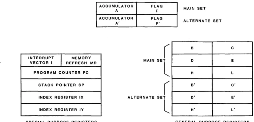
THE 2810 ACCESSIBLE REGISTERS
B.1 THE Z-80 PROGRAM ACCESSIBLE REGISTERS .... B-3 B.1.1 Accumulator and Flag Registers .... B-3 B.1.2 Special Purpose Registers ... B-3 B.1.3 General Purpose Registers ... B-4 B.2 THE 8250 ADDRESSIBLE REGISTERS ... B-5 B.2.1 Peripheral Control Register ... B-6 B. 2.2 Line Control Register ... B-7
APPENDIX C
APPENDIX D
APPENDIX E
FIRMWARE LISTING
PARTS LIST, BOARD LAYOUT, SCHEMATIC', SPECIFICATIONS Parts List . . . • . . . D-3 Board Layout . . . • . . . D-5 Schematic ...•...•...•. ' ..•.. D-7 Specifications . . . • . . . D-9
LIMITED WARRANTY
No manual can be everything to everybody. But we have tried to design this manual so that it will be a useful reference tool for most of its users. The chapters up to "Theory of Operation" contain the information you need to configure the boa~d to your system and to operate it with the provided firmware. "Theory of Operation" and the appendices are designed for those of you who want more information about the board, whether from curiosity or a desire to further customize it. Programming information on the Z-80 is not included in this manual; the information is simply too extensive. You will need to acquire a z-80 programming manual.
INTRODUCTION TO THE 2810 Z-80 CPU
California Computer Systems' 2810 Z-80 CPU provides you with a CPU, a master serial 1/0 port, and monitor firmware. As a result, it is the ideal foundation for an S-100 system; with the addition of RAM memory and a console device, you can have a complete system that allows considerable add-on flexibility. The
2810 Z-80 CPU is also an excellent choice for upgrading a present
system. It has been carefully designed to be compatible with the major S-100 systems on the market.
The 2810 CPU and CCS's line of S-100 peripheral boards are
designed to work uniquely well with each other. For example, the
2422 Multimode Floppy Disk Controller board contains ROM-resident
firmware which can overlay the CPU firmware with its own, changing the monitor firmware from a paper tape-oriented firmware to a floppy-disk oriented firmware. No reprogramming of ROMs is necessary; after a minimum amount of setup, the disk controller board can be plugged in and operated with the 2810 cpu.
1.1 THE CPU
The 2810 z-80 CPU is an S-100 bus compatible card designed
manufacturers, allowing the user of an S-100 system a wide choice of products. To ensure compatibility with these products, the 2B10 simulates as closely as possible the BOBO signals used on the S-100 bus.
Since this board will be used in a wide variety of systems and for a wide variety of applications, a number of optional features have been incorporated. These include a power-on jump for systems without front panels, address mirroring circuitry for BOBO system compatibility, and an M1 Wait State for slow memory. Moreover, bus signals for which possible bus conflicts exist are made jumper enabled.
Three diagnostic LEDs have been provided on the 2B10. One indicates that the ROM is enabled and selected. The second indicates that the CPU is executing a software Halt instruction and is waiting for an interrupt. The third LED indicates that CPU has been programmed to accept interrupts. Since the CPU will remain halted while executing a Halt instruction until the system is reset or the CPU receives an interrupt, the last two LEDi can be used in combination to detect the software problem of the CPU receiving a Halt instruction before it receives an Interrupt Enable instruction.
1.2 THE ASYNCHRONOUS SERIAL I/O PORT
SETUP AND INSTALLATION
The first section of this chapter deals with configuring the 2810 to meet your system's requirements. Those of you who do not plan to use the serial port and do not have a front panel can install the board in your system after having configured the board. If you do plan to use the serial port or a front panel, section 4.2 gives additional setup and installation procedures concerning the port, while section 4.3 gives information on installing this board in a front panel system.
2.1 BOARD SETUP
The 2810 CPU has a number of features which are enabled or configured through on-board plug jumpers'. Each of these features is discussed below, roughly in the order of the jumpers on the board, starting with the upper left corner of the board and proceeding clockwise. In addition to the plug jumpers, there is a switch to be set and an optional jumper that can be soldered in. If you are having difficulty locating or identifying any of the jumpers or the switch, the board layout in Appendix C should help.
2.1.1 Serial Port Enable and Address Select Jumpers
2.1.4 M1 Wait State Select Jumper
By setting the WAIT jumper to ON, you will force the CPU into one Wait state during every M1 Cop code fetch) cycle of an instruction cycle. In a Z-80, the memory access time requirements are strictest during an M1 cycle; the Memory Read and Write cycles allow an additional half a cycle to complete memory access. Thus by enabling the M1 Wait circuitry, you can use memories with access times half a clock cycle slower. In practice, this means that when the CPU is operating at 4 MHz, enabling the M1 Wait state circuitry slows the memory access requirements by approximately 110 nsecs; at 2 MHz it slows the requirements by approximately 220 nsecs. Theoretically, memories with access times slower than 400ns need a Wait state when the CPU is operating at 4 MHz. However, practice is often different than theory; you should experiment with the requirements of your system.
Most of CCS's memory boards do not need Wait states. All have provisions, however, for on-board Wait state generation, allowing Wait states to be inserted on an individual board basis. Thus you can slow down the processor for slow memory and allow it to run at full speed with fast. On-board Wait state generation can also be used fo~ ve~y slow memory: adding a Wait state by this method slows access times by approximately 250 nsecs at 4 MHz and 500 nsecs at 2 MHz. The disadvantage of on-board Wait state generation is that it adds a Wait state to every memory cycle in which the memory board is selected. You will have to experiment to discover which method, or combination of methods, is most efficient for your system. Note that the M1 Wait circuitry will also add a Wait state to Interrupt Acknowledge cycles, since the z-80's M1 control signal is active at that time. The WAIT jumper set to ON enables the M1 Wait circuitry.
2.1.5 Power-on Jump Enable and Address Select Jumpers
If enabled by the JMP EN jumper, the power-on jump circuitry forces the CPU to jump to the address set by the JMP ADDR SEL jumpers when your system is turned on or reset. If the circuitry is disabled, the processor looks for its first instruction at memory location OOOOh on power-on or reset. Should you enable the power-on jump circuitry, set the JMP ADDR SEL jumpers, JA15-JAO, to the binary value of the jump address you wish. Please note that JA15 is the high order bit; you should enter the binary address from the bottom up.
a jump to the beginning address of the on-board ROM, FOOOh, on power-on or reset. To do so, set JA15-JA12 to 1, JA11-JAO to 0, and JMP EN to ON.
2.1.6 2/4 MHZ Signal Enable Jumper
In the early BOBO systems, pin 9B of the bus was assigned to the .status signal sSTACK, indicating that a stack read or write was in progress. Some manufacturers of S-100 systems, noting that sSTACK is little used, have converted this line to a 2 MHz/4 MHz operation indicator, where a high indicates the processor is operating at 4 MHz. We have done so also. This is a convenient feature for those of you with front panels; the sSTACK LED will tell you at a glance at which frequency the CPU is operating. It also allows peripheral devices which can monitor this line to request Wait states only when the processor is operating at 4 MHz. The newly proposed standards for theS-100 bus, however, suggest using pin 9B for an error signal input, ERROR*. To avoid possible bus conflicts, we have made the 2/4 MHZ line jumper-enabled/disabled.
2.1.7 PHANTOM Enable Jumper
The PHANTOM line is used to overlay memory at a common address. On the the 2B10 Z-BO CPU, the PHANTOM line allows an external device generating the PHANTOM signal to overlay the ROM's memory space on a byte-to-byte basis. Such a device might be one of CCS's I/O boards. The ROMs on these boards can generate the PHANTOM signal, allowing portions of the CPU's firmware to be overlaid with the I/O boards' firmware. Thus driver firware for the I/O boards can be patched onto the CPU's firmware, without the CPU's ROM being reprogrammed.
Disable the signal if you do not plan to use it.
2.1.B NMI Enable Jumper
software commands. A nonmaskable interrupt request, on the other hand, forces the CPU to do a restart at address 0066h, regardless of the state of the Interrupt Enable flip-flop. On the 2810 board, the nonmaskable interrupt control input appears on pin 12 of the bus, as required by the proposed S-100 bus standards. However, since the 8080 processor "does not provide for nonmaskable interrupts, some systems may use pin 12 for another signal. To avoid bus conflicts, we have made the NMI line jumper-enabled/disabled.
2.1.9 REFRESH Enable Jumper
The Z-80, unlike the 8080, is designed to work with dynamic as well as static RAM. At the end of every M1 (op code fetch) cycle, while the CPU is busy decoding the current instruction, the Z-80's refresh register puts out a refresh address on the address lines and the control signal REFRESH goes active. If you have in your system a dynamic RAM board, such as CCS's 65K dynamic RAM board, that can use the REFRESH signal for refresh control, you should enable this line. Consult your memory manual. Some 8080 systems may have the REFRESH line, pin 66, assigned to another signal. If this is true of yours, disable this line.
2.1.10 2/4 MHz Toggle Switch
This toggle switch, located on the top right half of the board, allows you to select the operating frequency of the Z-80. The switch positions are marked on the board. The position of this switch should be set before you turn on your system or reset it. It should not be changed during system operation.
2.1.11 MREQ jumper
2.2 SERIAL I/O PORT SETUP
The following instructions apply only if you are planning to use the serial port.
2.2.1 I/O Cable Installation
CC8 does not supply the cable assembly that plugs into J2,
the serial port's connector. You will have to obtain one.
The mating connector for J2 is a standar~ flat ribbon cable
connector; the other end of the cable requires a OB-258
connector. If you assemble the cable yourself, be careful not to
twist it; the pin 1 strip on the ribbon cable (usually the
colored outside strip) should match pin 1 on both connectors.
Plug the cable assembly into J2, matching pin Is. (Pin 1 for J2
is labeled on the board). Push the cable connector down firmly
until you can no longer see the metal pins. The OB-258 connector
should be fastened to one of the slots in the back of your
mainframe. Plug the OB-25P connector on your peripheral's signal
cable into it.
2.2.2 Peripheral Configuration
If you plan to use the I/O driver and initialization
firmware provided, your peripheral should be set to expect a
serial data format of 8 data bits, no parity bit, a 0 stick bit
and one stop bit per word. 8et your peripheral for the baud rate
at which you wish to operate; the firmware will initialize the
port to any standard baud rate. Consult your peripheral manual
for setup instructions.
If you are not using the initialization firmware provided,
you will have to configure your peripheral to match your
2.3 FRONT PANEL SETUP
If you will be using the 2810 in a front panel system, you must connect the data cable from the front panel to the front panel data socket, J3. S~cific instructions for the Altair and Imsai microcomputers follow.
2.3.1 ALTAIR 8800
You must replace the molex connector on the front panel cable with a DIP plug that you supply yourself. Be careful when soldering the connections: Unlike the data lines on J3, the data lines on the Altair molex connector are not arranged sequentially.
2.3.2 IMSAI
THE MOSS 2.2 MONITOR
CCS's MOSS 2.2 Monitor contains powerful routines for program debugging and for controlling from a console keyboard a system using the 2810 Z-80
cpu.
It allows you to display a block of memory in hex and ASCII, to move, change, and verify memory, and to transfer control to another program in memory with breakpoints set. You can also output or-input a data byte to or from any 1/0 port and command the monitor to read, write, and format paper tape.Note that for the MOSS Monitor to work exactly as described below, the on-board ROM, serial 1/0 port, and power-on jump circuitry must be enabled, with the serial port's base address set to 20h and the jump address set to FOOOh.
3.1 THE MONITOR'S MEMORY SPACE
3.2 SOFTWARE ENTRY POINTS
A cold-start entry at FOOOh sets up the system stack and work area, initializes the serial port and register storage area, selects the on-board serial port as the console interface, and loads memory locations OOOOh-0003h with a jump instruction to the warm-start routine. It also loads the following locations, called by the Z-80 restart commands, with jump vectors to a restart error message: 0008h-OOOAh, 0010h-0012h, 0018h-001Ah, 0020h-0022h, 0028h-002Ah, 0030h-0032h, and 0038h-003Ah. These locations can be overwritten with restart routines.
A warm-start"entry at F10Fh resets the stack pointer and the warm start jump vector located at 0000-0002h. All other conditions remain unaffected.
The breakpoint entry at F024 saves all register contents; all other conditions remain unaffected.
3.3 THE BASIC 1/0 ROUTINES AND THE IOBYTE
You can call the monitor's basic 1/0 subroutines from your own programs. The jump vectors are as follows:
Routine name
CONIN CONOUT CONST READER PUNCH LIST
Address
F003 FOOg F012 F006 FOOC FOOF
Description
Console input Console output Console status
Paper tape reader input Paper tape punch output List device output
These routines perform the IOBYTE handling to support the IOBYTE function, as developed in the Intel MDS system and as used by CP/M.· The IOBYTE function allows you to assign a physical device to one or more of four logical peripheral device categories: Console, Punch, Reader, and List. The current physical to logical device assignment is stored in the IOBYTE in location 0003h. When an 1/0 routine, such as CONIN, is called, it examines the contents of IOBYTE and jumps to the peripheral driver routine indicated by the physical device assignment. The contents of the IOBYTE, and hence the physical device assignments, can be changed through the Assign command.
only the teletype physical ass~gnment in all four logical categories. (Please note that the physical assignment names do not have to accurately describe the actual peripheral used. The teletype assignment, for example, could be used to implement console operations with a CRT.) All other physical assignments cause a jump to the I/O Assignment Error message when. one of the above routines is called. For more information, see the Assign command, 3.7.1.
With the exception of CONIN, the above basic I/O routines are CP/M compatible when used with the default teletype assignment. They conform to the CP/M calling conventions, passing the data in the C register for any output and in' the A register for any input. For a CP/M compatible console input routine, use entry point F68Fh. This routine, CONI, strips the ASCII parity bit as CP/M convention requires.
3.4 BRINGING UP THE MONITOR
To enter the monitor, turn your system on or reset it. This results automatically in a cold-start entry into the monitor. Set your terminal to the bauct' rate at which you wish to operate. You have a choice of any baud rate between 2 and 56K baud. Hit
the carriage return key until the monitor responds with
MOSS VERS 2.2
The maximum number of carriage returns needed before the monitor responds is three. When the monitor prompt appears, you may start entering commands.
3.5 MONITOR COMMANDS
The MOSS Monitor commands must conform to a specific format. The general form is
-CE1 E2 E3
The Command one-character response to is allowed character.
Character: The monitor is controlled by commands entered from the keyboard in the monitor prompt, a dash (-). No space between the prompt and the command
Address and data entries: The general form for an address is a four digit hex number; for data, a two digit hex number. Leading zeros need not be entered; the monitor will supply them. No space is allowed between the command character and the first address or data entry. Subsequent entries must be separated by a delimiter. The monitor looks at only the last four address characters or last two data characters before a delimiter. So if you make
a
mistake while typing an entry, keep typing until the last two or four characters are correct.Delimiters: The MOSS Monitor recognizes three deli-miters: a carriage return (CR), a space, or a co~ma. A carriage return indicates to the monitor that the current command is complete and should be executed. Either a space or a comma can mark the end of an address or data entry. In our command examples we will generally use a space as a delimiter, unless a comma makes the command form clearer. Please note, however, that you can use the space and the comma interchangeably. In certain commands a space or a comma can also be interchanged with a carriage return. These are commands for which the Monitor expects a fixed number of entries (and hence delimiter~)
following the command character.
Sample Command
The following commands to display the block of memory OFFBh to 100Ah are all equivalent. Although the spacing is not form free, some variety in the command form is allowed. Note that the display command requires two and only two address parameters, so that the last delimiter can be a comma or a space as well as a carriage return.
3.6 ERROR MESSAGES
The MOSS monitor detects three types of error conditions and responds with a different error message for each. They are as follows:
Command Error: Should you make an invalid entry, the command will be aborted, a warm boot of the system will occur, and the error message
????
will be printed, followed by the monitor prompt.
1/0 Assignment Error: As described in section 3.3, the Assign command allows you to assign a physical device to a logical peripheral category. When an 1/0
routine involving the logical category is called, the CPU will jump to the driver routine indicated by the physical assignment. If there is no driver routine, it will jump instead to the 1/0 Assignment Error routine. This routine sets the IOBYTE to its default value, outputs the error message
1/0 ERR
and does a warm boot of the system. If you are using the monitor's basic 1/0 routines with CPIM, an 110 assignment error will cause the error message to be printed and control returned to CP/M. See the Assign command for more detail.
Restart Error: During cold-start initialization, jump-vectors to a restart error message are loaded in the memory locations called by the 2-80 restart instructions. This is done to prevent a program jump to a restart address without code. A restart error causes a warm boot of the system and the following message to be printed:
RST ERR
3.7 COMMAND DESCRIPTION
3.7.1 Assign (A)
The Assign command allows you to change the physical-to-logical device assignments and thus choose the peripherals you wish to work with while in the monitor. The IOBYTE function as developed by Intel for the MDS systems divides peripherals into four logical categories: Console, typically a teletype or a CRT; Reader, a paper tape reading device; Punch, a paper tape punching device; and List, a hard-copy printing device. Each of the four logical categories may have one of four physical devices assigned to them. The possible physical-to-logical assignments are as follows:
(C) Console Logical Device (T) Teletype
(C) CRT
(B) Batch Mode (input from logical reader device; output to logical ~ist device) (1) User Console #1
(R) Reader Logical Device (T) Teletype
(P) Paper tape reade~ (1) User reader #1 (2) User reader #2 .
(P) Punch Logical Device (T) Teletype
(P) High speed paper tape punch (1) User punch #1
(2) User punch #2
(L) List Logical Device (T) Teletype
(L) High speed line printer (CRT in CP/M)
(1) User list #1 (High speed line printer in CP/M) (2) User list"#2 (User List #1 in CP/M)
To assign a peripheral to a logical device category, enter
-AX
logical device code, the computer will return immediately with a prompt for the physical device code. Enter
-y
where Y equals the physical device code. Should you enter a delimiter only or a nonvalid device code, the device assignment will remain unchanged.
EXAMPLE:
Entering
-AR-P
assigns a high speed paper tape reader to the Reader logical device category.
Assigning a physical device to a logical category alters the contents of the IOBYTE, stored in location 0003h. Every time an input or output routine involving a specific logical device is performed, the I/O routine examines the contents of the IOBYTE to determine the physical device assignment and jumps to the driver routine called by the physical assignment. If there is no driver routine, the I/O routine jumps to I/O assignment error routine, resulting in the I/O Assignment Error message being output and physical assignments being set to their default value, the teletype.
For all the basic 1/0 routines, the teletype assignment forces a jump to the on-board serial port drivers. The serial port is designed to be the console interface; it is best used for a CRT, although any console device can be used. Please note the port drivers cannot drive the paper tape reader or punch of a teletype. If you have not altered the firmware in any way, calling the Reader or Punch I/O routines results in the CPU reading from or writing to the console device when the teletype assignment is used.
None of the other physical device assignments are supported by driver routines. You can patch driver routines for different devices onto the monitor firmware by two techniques. One is to have the routines residing in a ROM device capable of generating the PHANTOM signal (section 2.1.8), so that the jump instruction
to the I/O error message for a particular physical device
The second technique is to change the jump instruction in the ROM itself. For example, if you wished to connect a line printer to your system, you would change the jump instructions at locations F61D and F676 so that they contained the starting addresses of your driver routines and not the address of the 1/0
error message. This, of course, means erasing and reprogramming the ROM.
3.7.2 Display (D)
This command allows you to display the contents of a specified block of memory. The general form for the command is
-DA1 A2
where A1 and A2 are the first and last bytes, respectively, of the memory block.
The resulting display divides the memory into 16 bytes per line. Each line starts with the address of the first byte in the line, followed by the data in hex and their ASCII equivalents. The contents of locations having the same last hex digit in their address are aligned vertically. Periods represent data for which there are no ASCII equivalents. As the output fills the screen, it will automatically scroll up. To freeze the display, type a control-So To start it again, hit any key on the keyboard. Should you wish· to escape from the display mode, hitting any key on the keyboard will abort the command and cause the monitor prompt to appear.
EXAMPLE
Entering
DF450 F4BF
results in the following display:
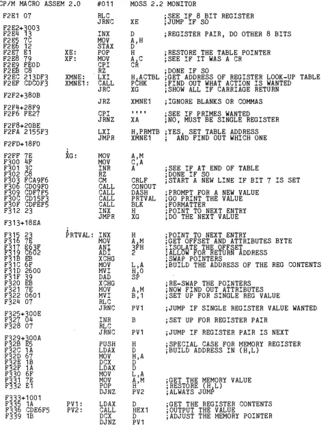
F453 F460 F470 F480 F490 F4AO F4BO F4CO
E1 08 09 01 C1 F1 E1 F9 00 21 00 00 C3 00 00 AF 32 03 00 21 6C F4 C3 B5 F6 49 2F 4F 20 45 52 02 CD E8 F6 BO 47 82 57 78 C9 DE 00 CO 7C F6 DE OA C3 7C F6 CD 56 F6 E6 7F C9 3F 3F 3F BF 40 4F 53 53 20 56 45 52 53 20 32 2E 32 00 8A 3E OF 03 24 11 40 00 62 6A DB 26 A3 28 FB DB 26 23 A3A3 C2 AD F4 E5 29 5C 19 19 E5 29 29 DB 20 2B 7D B4 C2 BO F4 E1 3E 83 03
a. YQAqay. ! .• C
• • /2 • • ! 1 tC5vIIO
ERRMhvOG.WxI •• MI
v •• ClvMVvf.I???? MOSS VERS 2.2 •• ) • S$ .@. bj [&11 ( f [&11
##B-te)\ •• eJJ[ +
3.7.3 End Of File (E)
The E command informs the computer to type punch an Intel format End Of File record at the end of a just-punched paper tape file. The Intel EOF format contains both the entry address for the file and six inches null leader. The E command allows you to specify the entry address and change the length of the leader, if you wish. The general form for the command is
-EA L
where A is the entry address and L is the length of null leader in tenths of inches expressed in hex. For example, for a 'four inch leader, enter hex 28 (4"=40 tenths=28h). The default value for the length is six inches; for the address, OOOOh. An entry address of OOOOh will return control to the monitor after the paper tape has been read.
The Monitor expects two parameters for the E command. A carriage return after the E or first parameter will result in the error message ???? If you wish to set the length and entry address to their default values, simply enter a space or a comma twice.
If you have assigned to the logical punch category a physical punch device for which there is no driver code, using the E command will result in the error message
1/0 ERR
and the return of the monitor prompt. The exception for this is the teletype default assignment. The firmware is designed to output the EOF record to the console device.
3.7.4 Fill (F)
The fill command allows you to fill a block of memory with a specified constant. The general command form is
EXAMPLE
Entering
-F10AA 10BB
fills the memory block 10AAh to 10BBh with the constant 1.
3.7.5 Goto (G)
The G command allows you to transfer control from the monitor to another program. It allows you to specify the entry address and to set up to two breakpoints for returning control to the monitor. When the monitor encounters a breakpoint, it saves the contents of the z-80 registers in the system's temporary storage and outputs to the console device an asterisk followed by the next address in the program. It then returns the prompt. You can use the Examine Register command (X) at this time to examine or change the saved registers.
The general form for the G command is
-GA B1 B2
where A is the entry address, and B1 and B2 are the addresses of the breakpoints. There are many allowed variations on this command, however, which makes it a powerful and convenient
command. You have the option of establishing 0, 1, or 2
breakpoints: simply enter a [CR] when you have established the number of breakpoints you wish. If you enter the maximum, two, a delimiter (comma or space) is all that is necessary to begin command execution.
You may also begin execution of the program at the PC address saved in the register storage area. Thus you can return
control to the address where the program stopped when it
encountered a breakpoint, or to the address you have loaded in the saved PC register through the Examine Register command. Note that since all breakpoints are cleared when any breakpoint is encountered, you must specify any desired breakpoints in the command if you use it this way. The form of the command for transferring program control to the address in the PC register is
-G[CR] (no breakpoints) or
-G,B1,B2 (breakpoints set)
to be mentioned. Because breakpoints are generated by the monitor inserting a RST 8 instruction (CF) into the program at the breakpoint location, breakpoints can be set only in programs residing in RAM. Further, a breakpoint must be inserted at an op code location. If it is inserted in an operand or data field, it will not be executed.
3.7.6 Hex Number Addition (H)
This command provides an easy way to add or subtract hex addresses. Entering
-HA1 A2
where A1 and A2 are the hex addresses results in the output
AS AD
where AS=A1+A2 and AD=A1-A2. Note that if the sum is greater than FFFF, the carried one is lost. If A2 is greater than A1, A2 will be subtracted from A1 + 10000h.
3.7.7 Input (I)
This general purpose input command allows you to read a data byte from any input port. To do so, enter
-IA
where A is the port address in hex. The monitor will respond by printing the data byte in binary.
3.7.8 Leader (L)
The L command allows you to output hex-number nulls for a paper tape leader. As with the E command, you may specify len~th
of the leader in tenths of inches in hex, the default value being six inches. The form for the L command is
-LH
If the current physical-to-logical assignment for the Punch category is the teletype, the null leader will be output to the console device unless punch driver routines have been provided for the teletype assignment.
3.7.9 Move (M)
The M command moves a block of data to a specified address. The general form for the command is
-MA1 A2 AD
where A1 and A2 are the addresses of the first and last bytes of the memory block and AD is the destination address.
When using this command, be careful not to locate the destination address within the source block. Since the block is moved byte by byte, starting with the byte with the lowest address, the data being transferred will write over the original contents of the section of the source block that follows the destination address.
3.7.10 Output (0)
This general purpose output command allows you to output a data byte to any output port. Enter
-OA D
where A is the port address and D is the data in hex.
If you have CCS memory boards in your system, you can use this command to select a memory bank by outputting a Bank Select Byte to the Bank Select Port. (See your memory board manual.)
3.7.11 Query (Q)
The Q command device assignments.
displays the current Entering the command
-Q[CR]
results in the current assignments being displayed in the format
C-X R-X P-X L-X
where X equals the physical device code.
3.7.12 Read (R)
The read command allows you to read from an Intel format paper tape in the currently assigned paper tape reader and to add a bias to the starting address in the paper tape header. The general form for the read command is
-RB
where B is the address bias in hex.
The monitor checks for errors while reading the paper tape. If it encounters one, the program is aborted. The read routine also provides error checking of the program loaded in memory; if an error is found, the address of the byte in error is displayed, along with an 8-bit binary representation of the bit error, in which a 1 indicates a bit in error. For example, the display
F038 00010000
would indicate that bit 4 of the byte in memory location F038 is in error.
After the paper tape has been read, control will be returned to the monitor if the entry address in the EOF record is zero. If it is a non-zero number, control is transferred to that address.
If the current physical device assigned to the Reader
logical category is the teletype, the monitor will respond to the Read commmand by reading a a program in binary typed by hand from the console unless you provide paper tape reader rountines for the teletype assignment.
3.7.13 Substitute (S)
-SA,
where A is the address of the memory location you wish to examine. The computer will immediately respond with the data contents followed by a prompt:
-SA,D-If you wish to leave the data unaltered, simply enter a
delimiter. If the delimiter is a space or a comma, the computer will respond with the contents of the next consecutive memory location and another prompt. If it is a carriage return, the command is terminated and control is returned to the monitor. Should you wish to alter the data, enter the desired data
followed by a delimiter: a carriage return if you want to terminate the command or a space or a comma if you wish to review
the next memory location. You can continue examining and
altering memory byte by byte in this way as long as you wish. To make it easier for you to keep track of where you are, on every 8-byte boundary (that is, an address ending with either 0 or 8, the monitor will do a line feed and print the address along with the data.
3.7.14 Test (T)
hard RAM.
The test command provides a quick way to test RAM memory for data bit failures without destroying the contents of the To test a block of memory for bit failures, enter
-TA1 A2
where A1 and A2 are the addresses of the first and last bytes in the block, respectively. The monitor will respond by printing
the address of any byte in error, followed by an 8-bit
representation of the bits in error. (See the Read command for further details). If you wish to freeze the display type a Control-So To start it again, hit any key. Hitting any key while the command is executing returns you to the monitor.
3.7.15 Verify (V)
You can use the V command to compare two blocks of memory and verify that they are the same. Type
where A1 and A2 are the addresses of the first and last byte in the source block and AD is the starting address of the block to be verified. Should the two blocks match, the monitor will return
with the prompt. Should two correspondng bytes differ, the
monitor will display the source address and its contents in hex, followed by a dash and the contents of the correRponding address
of the block being verified. During the execution of the
command, the display can be frozen or control returned to the monitor as described in previous section.
3.7.16 Write (W)
Use the W command to punch a memory block on paper tape. Enter
-WA1 A2 R
the first and last byte of
The Intel paper tape
16 data bytes. You can from 1 to 255. Enter value is 16 data bytes. with this command.
where A1 and A2 are the addresses of the block and R is the record length.
format specifies a record length of
change that length to any number of bytes the length you want in hex. The default Note the monitor expects three delimiters
If you want a null leader to begin your file, you must use the L command before the W command. If you want to end your file with an EOF record or null leader, use the E or L command after the file has been punched.
Again, the monitor w~ll output the memory block to the console device if the logical punch category is at its default value and no driver routine has been provided for the teletype punch assignment.
3.7.17 Examine (X)
The X command is a very useful command when
conjunction with the G command's breakpoint facilities.
-X[CR, space or comma]
used in Entering
Interrupt register (I), the Program Counter register (P), the Stack Pointer register (S), the two Index Registers (X and Y) and the Refresh register (R). In addition, the contents of the memory locations addressed by the main and alternate Hand L registers are also displayed (M and M'). The re~isters are displayed in the following four-row format
A-xx B-xx C-xx D-xx E-xx F-xx H-xx L-xx M-xx P-xxxx S-xxxx I-xx
A'-xx B'-xx C'-xx D'-xx E'-xx F'-xx H'-xx L'-xx M'-xx X-xxxx Y-xxxx R-xx
where xx equals a two digit hex byte and xxxx equals a four digit hex address.
To examine or alter the contents of one register, enter
where r is a (Note that must preface
monitor will prompt:
-Xr[CR, space or comma] or
-X'r[CR, space or comma]
main register and 'r is an alternate register. if you wish to examine the X, Y, or R registers, you register character with the prime mark.) The return with the contents of the register and a
-Xr,Dh-As in the substitute memory command, you have the option of altering the memory (entering desired contents followed by a delimiter) or leaving the contents unchanged (entering a delimiter). A carriage return terminates the command; a space or a comma causes the contents of the next register to be displayed. Note that altering the contents of the Hand L registers changes the address; if you wish to alter the contents of the memory location, alter the M register. (See section B.1 for a discussion of the Z-80 registers.)
3.7.18 Initialize Baud Rate (Y)
To change the baud rate of your system without a system reset, use the Y command. Enter
-Y (no delimiter)
prompt. The monitor will accept any baud rate between 2 and 56K baud.
3.7.19 Zleep (Z)
The Z command is used to prevent unauthorized use of your system. Entering
-Z[CR, space or comma]
THEORY OF OPERATION
This chapter is divided into two main sections: the CPU and
the Serial Port. In both sections, active low signals are
indicated by an asterisk (*) following the signal name.
Definitions of the signals used by the CPU bus and the serial interface can be found in Appendix A.
4.1 THE CPU
This section describes the 2B10's support circuitry for the
z-BO. Where it is pertinent, we discuss the z-BO's operation. However, a complete description of the Z-80 is beyond the scope of this manual. Should you wish to know more about it, we suggest you consult a Z-BO technical manual.
Since the S-100 is an BOBO-oriented bus, much of the
circuitry in the 2B10 z-BO CPU is devoted to interfacing the z-BO
to the S-100 bus. Because of this, and because this board will be used in BOBO-based systems, the following discussion of the
2B10's operation will often deal with the differences between the
BOBO and the Z-80.
4.1.1 The Reset Logic
The gates generating connected in series, so that
low, which in turn pulls
approximately 50 msecs after a one-shot which emits a
POC*, pRESET*, and EXT CLR* are
when POC* goes low, pRESET is pulled
EXT CLR* low. POC* goes low
power-on. This pulse is inverted and pulls POC* low. Both pRESET* and EXT CLR* can also be pulled low by external switches.
4.1.2 The External Clock Circuitry
The early 8080 microprocessor required a 2 MHz, two-phase,
nonoverlapping clock. Thus, by convention, there are three
clocks on the S-100 bus: CLOCK, which is a 2 MHz signal; phase
one, $1; and phase two, $2. The Z-80, on the other hand, can operate at either 2 or 4 MHz and requires only a one-phase clock. Thus the functions of the $1, $2, and CLOCK signals on the 2810 differ from those on an 8080 CPU. On the 2810, $1 and $2 can be -either 2 MHz or 4 MHz signals. Once inverted, $2 is the processor's clock, pCLK,. while $1 is available on the bus simply for those devices that need it. CLOCK remains a 2 MHz signal, regardless of processor speed, for those devices that need a clock of a constant frequency.
The clocks on the 2810 are derived from the on-board 16 MHz crystal oscillator. The 16 MHz signal is divided by 2, 4, and 8 by a synchronous 4-bit counter, U24. Thus the outputs of this counter are in-phase 8 MHz, 4 MHz, and 2 MHz signals. These
si~nals are multiplexed by U22, a 4-to-2 line multiplexer. The
select line for the multiplexer is controlled by the 2/4 MHz toggle switch. When the switch selects 2 MHz, the multiplexer's outputs are the 2 and 4 MHz signals. The 2 MHz signal is the $2 clock and is inverted and buffered to become pCLK. The 4 MHz signal is inverted and ANDed with the 2 MHz signal, creating the non-overlapping $1 clock (see figure 4-1). When l~ MHz operation is selected, the multiplexer's outputs are the 4 MHz and an 8 MHz signals, which, through the process described above, become the 4 MHz $1, $2, and pCLK signals.
4.1.3 The Address Bus and Address Mirroring
The Z-80's low-order address lines are buffered by a three state bus driver, the outputs of which are bus address lines AO-A7. They are also multiplexed with the z-80's high-order address lines by U28 and U29, the outputs of which are the bus address lines A8-A15. The select line to the multiplexers is
controlled by the address mirroring circuitry. When it is
enabled through the address mirror jumper, it will pull the select line hi~h, allowing the low-order address bits onto the
hi~h-order address bus whenever the I/O request signal from the
(An Interrupt Acknowledge cycle isdistinquished by both signals being active.) In any other case, or if the address mirror circuitry is disabled, the select line to the multiplexer will be
low, allowing only the high-order address bits onto the
high-order address bus.
The signal ADD DSB*, when active during DMA operations, places the address bus driver and multiplexers in their high impedance state, allowing an external device to control the address bus without interference from the CPU.
4.1.4 The Data Out and Data In Busses
During pSYNC's active period, status bits must be available on the Data Out bus. On the 2810, this is accomplished by multiplexing the Status signals with the data lines from the
2-BO. The output of the multiplexers is the Data Out bus,
DOO-D07. The signal pSYNC controls the state of the select
lines. When pSYNC is active high, the status bits are
multiplexed onto the Data Out bus. When pSYNC is inactive low, the data bits are multiplexed onto the Data Out bus. The Data Out bus can be placed in its high impedance state by DO DSB* for DMA operations.
The Data In bus is buffered by an B-bit, three-state bus driver. This driver is disabled whenever pDBIN is inactive, except :during DMA operations (indicated by the active BUS ACK*).
It is also disabled under a number of other conditions. When either the ROM, the serial port, or the power-on jump circuitry is enabled, the driver is disabled, since data will be passed to the CPU on the internal bi-directional data lines. Front panel examination of memory will also disable the Data In bus while the front panel is commanding the CPU through the front panel data lines to fetch the data.
4.1.5 The Control Signals
Because the S-100 is an BOB a-oriented bus, the signals on its control bus are generally the functional equivalents of the control signals of the BOBO itself. Thus the 2B10 2-Bo CPU must
emulate the BOBO's control signals if it is to be S-100
BOBO-like control outputs from the z-BO outputs. The following section describes how each 80BO control output is emulated by the 2B10.
pSYNC In an 80BO system, this signal is generated by the processor during T1 (the first clock cycle) of every machine cycle and indicates to external devices that they can read the current status of the processor on the data bus.
The z-80 has no equivalent signal; pSYNCH must be
generated entirely through external circuitry. On the
2B10 CPU, it is generated primarily by two flip-flops, one to generate pSYNC and the other to turn it off. The first flip-flop, U35b, is clocked by the rising edge of either the inverted M1*, MREQ*, or IOREQ*--whichever goes active first in a bus cycle. It is set by the state of the REFRESH* line: only when REFRESH* is inactive high will pSYNC, the Q output of the flip-flop, be high. This prevents pSYNC from being generated during the l~tter part of an M1 cycle when MREQ* goes low again with the signal REFRESH*. So that it can be turned off, pSYNC is input to the second flip-flop, U35a. When U35a is clocked, its Q* output clears U35b, turning off pSYNC. This flip-flop is clocked by the $2 clock during cycles in which M1* or IOREQ* is active and by the inverted $2 during bus cycles in which MREQ* only is active, causing pSYNC to last approximately one clock cycle in any bus cycle, as it does when generated by an BOBO. Note that during an 1/0 cycle, pSYNC occurs during T2, instead of T1, since IOREQ* goes
active then (see Fiqure 4-1). Its function remains
exactly the same, however; it still marks the beginning of the bus cycle and indicates that valid status bits are on the bus.
pWR* PWR* indicates that valid data is present on the data bus and thus becomes active after pSYNC. The Z-BO's write control output, WR*, serves the same function as pWR*; it simply needs to be disqualified during the active pSYNC. Flip-flop U34b serves this purpose. The flip-flop, its D input tied high, is clocked on the falling edge of pSYNC and cleared on the rising edge. Thus its Q* output will be low only when pSYNC is inactive. The Q* output is ORed with WR*. Only if both signals are low will the output of the OR gate, pWR*, be active low. See Figure 4-1.
pDBIN In 80BO-based S-100 systems, pDBIN indicates that the data bus is conditioned to accept data from external devices. It goes active with the falling pSYNC signal and occurs
<1>2
pSYNC
pOBIN
REFRESH
T1 T2 T3 T4 T1 T2 T3 T1 T2 TW1 T3
~
U-
L J
L J
U-
L J
U-U-
~
U-
U-'1
n
n
~
, ,
n
,
~
~
U
I
l
I
U
,
I
,
I
L
l
I
Lr
\
I
1 The Z-80 automatically inserts a Wait state in every I/O cycle
FIGURE 4-1 TIMING WAVEFORMS FOR SELECTED CLOCK AND CONTROL SIGNALS
~
I
[image:37.794.59.733.81.466.2]2810, the Z-80's Read signal, RD*, is inverted and ORed with sINTA, producing pDBIN. Thus pDBIN will be active whenever either RD* or sINTA is active. Note that pDBIN is not disqualified by pSYNC; during a Read cycle it will be active while pSYNC is active (see Figure 4-1). This allows a longer memory access time, yet causes no bus conflict. During the time pSYNC is active, the Data In Bus and the internal data line~ are not being used, the status bits having been gated onto the Data Out bus from the status lines themselves.
pINTE The signal pINTE indicates the state of the
processor's internal interrupt enable flip-flop. The
8080 generates this signal itself; on the 2810 board it is generated by an external flip-flop, U14a, since the z-80 has no equivalent signal. The state of the z-BO internal
interrupt flip-flop can be set by the EI (Enable
Interrupts) and DI (Disable Interrupts) commands. In
binary these commands are 1111 1011 and 1111 0011. Note that these commands are distinguished by the state of bit 3 only. The rest of the bit pattern is the same. U32 monitors the data lines DO-D2 and D4-D7 for the EI/DI bit pattern. When it occurs, U32 enables flip-flop U14b, allowing it to be clocked by M1* going inactive. When U14b is clocked, its Q output in turn clocks U14a. If D3 is high, the output of U14a, pINTE, will be set high and the Interrupt Enable LED lit. If D3 is low, pINTE will be low. U14a is cleared and pINTE made inactive low by either the active pRESET* or sINTA. Thus the state of pINTE can be changed only by an EI or DI op code, a system reset, or an Interrupt Acknowledge. It should therefore accurately reflect the state of the processor internal interrupt flip-flop.
pHLDA pHLDA goes active in an 80BO system in response to a HOLD request, indicated by the active pHOLD*. In the Z-BO, there are two equivalent signals, BUSRQ* (Bus Request) and BUSAK* (Bus Acknowledge). Thus on the 2B10, BUSAK* is simply inverted to create pHLDA.
pWAIT The signal pWAIT indicates that the processor has entered a Wait state. The Z-BO has no equivalent signal. On the 2810 this signal is generated by the Wait state flip-flop,
U34a. This flip-flop is preset every time a device
state of its Wait input only on the falling edge of pCLOCK during T2. A device must make its first Wait request then or the CPU does not recognize it.
4.1.6 The Status Bus
The status bus on the S-100 bus communicates to external devices the current state of the processor--i.e, what bus cycle it is in--and qualifies the nature of the address on the address lines. At the beginning of each instruction cycle, the BOBO puts the 8-bit status information from its internal register out on the data bus where it can be sampled by external devices. The active pSYNC indicates its stable presence on the bus. At the same time the status information is latched in the external status latch to generate the status bus signals. The meaning of the status bits are summarized in the table below.
DATA BUS BIT 07 06 05 04 03 021 01 DO
STATUS BIT MEMR INP M1 OUT HLTA WO INTA
Instruction Fetch 1 0 1 0 0 x 1 0
Memory Read 1 0 0 0 0 x 1 0
Memory Write 0 0 0 0 0 x 0 0
Input Read 0 1 0 0 0 x 1 0
Output Write 0 0 0 1 0 x 0 0
Interrupt Acknowledge 0 0 1 0 0 x 1 1
Halt Acknowledge 1 0 0 0 1 x 1 0
1 In 8080 systems 02 is the STACK bit. On the 2810 sSTACK Is not generated. See 2.1.6.
TABLE 4-1 STATUS WORD DEFINITIONS
Because the status of the z-BO can be decoded from the control outputs themselves, the Z-BO has no internal status register. Therefore, the S-100 Status lines must be generated from the control outputs. When pSYNC is active, the status lines, with two exceptions, are gated onto the data bus by the bus multiplexers. Two of the status lines, sWO* and sINTA, will not always be active when pSYNC is active. The WO and INTA status bits must be generated separately.
sINTA This signal indicates that the CPU has accepted an
interrupt and is awaiting instruction from the
interrupting device. The z-Bo indicates an Interrupt
[image:39.623.81.530.333.458.2]strobe for this cycle. The bus signal sINTA is generated by ANDing the inverted signals M1* and IOREQ*. Thus sINTA
will be hi~h only when IOREQ* is active. This is
important since the 2810 uses sINTA to generate the bus Data In strobe, pDBIN, during an Interrupt Acknowledge cycle. However, sINTA generated this way does not become active until T3--too late to be gated onto the Data Out bus by pSYNC. Therefore the INTA status bit is generated by the inverted M1* being ANDed with RD*. Only when RD* is inactive high will the INTA bit be high. Since an active M1* occurs without an active RD* only during an Interrupt Acknowledge cycle, the state of the INTA bit accurately reflects the bus cycle.
sWO* When active low, sWO* indicates that the CPU is in a Write cycle. On the 2810 board, sWO* and the status bit WO are generated by two different methods. The status signal is simply the Z-80's WR* signal. However, WR* goes active low during T2 of a Memory Write cycle--too late to be present on the data bus when pSYNC is active. Thus the status bit
wo
is generated by either MREQ* or IOREQ* being active while RD* is inactive. Only during an 1/0 or Memory Write cycle would RD* be inactive. The method by which the status bit WO* is generated cannot be used to generate sWO*, since sWO* would then be generated during an Interrupt Acknowledge cycle.sHLTA sHLTA and the z-80 HALT* both indicate that the CPU has received a HALT instruction and is awaiting an interrupt. Thus sHLTA on the 2810 board is the inverted HALT*. The active sHLTA lights the Halt Acknowledge LED.
sOUT Indicating that the CPU is outputting data to an 1/0
device, this signal is generated when both IORQ* and WR* are active.
sM1 This signal is active during the Op Code Fetch cycle of an
instruction execution cycle and during an Interrupt
Acknowledge cycle in both the 8080 and Z-80. Thus sM1 is generated by the inverted M1* of the Z-80.
sINP Indicating that the CPU is reading data from an 1/0
device, this si~nal is active when both IORQ* and RD* are active.
4.1.7 The Wait Circuitry
The WAIT* input to the Z-80 is low when any of the following four conditions occurs: 1) the XRDY line is pulled low; 2) the pRDY line is pulled low; 3) M1* is active when the M1 Wait states are enabled; 4) the ROM is enabled when the Z-80 is operating at 4 MHz. U21c monitors for these conditions, its output going high whenever one of them is met. This high is inverted and pulls the Preset line to the Wait flip-flop, U34a, low. The resulting low on the flip-flop's Q* output pulls the WAIT* input to the Z-80 low. Q* will remain low as long as U21c continues to pull the Preset input to the flip-flop low. As soon as U21c releases the Preset line, the flip-flop will be reset when it is clocked by the rising edge of the 8 MHz clock from U24.
The 8 MHz clock is used to ensure that one and only one Wait state is generated per cycle in which the M1 or ROM Wait state circuitry is active. A Wait request from either circuit is qualified by pSYNC; only if pSYNC is active will U21c be pulled high. In most memory cycles, qualifying the signal with pSYNC ensures one Wait state per cycle. However, during an M1 cycle, pSYNC goes inactive before T2. Resetting the Wait flip-flop with the 8 MHz clock allows WAIT* to remain active long enough for the CPU to sample it, but not so long as to generate an extra Wait state.
4.1.8 The Rom Enable Circuitry
Address lines AO-A10 from the Z-80 are input directly to the ROM, since eleven address bits are necessary to select one location out of 2K. Address lines A11-A15 are input to the Address decoding ROM, U9, along with MREQ* and PHANTOM*. When U9 receives address bits on the high order address lines in the
4.1.9 Power-on Jump Circuitry
The power-on jump circuitry works by placing on the data bus the unconditional jump command C3 (11000011) during the first M1 cycle after power-on or a system reset and the low byte and high byte of the jump address during the two memory read cycles that follow a jump instruction. Because the Power-on Jump circuitry, when enabled, disables the Data In bus, there is no conflict with memory.
The correct order and timing of the command and address bytes are achiev~d through the use of four D-type flip-flops and two 8-line-to-4-line multiplexers. The flip-flops are used as a 4-bit shift register, the Q output of one flip-flop being tied to the D input of the next. The flip-flops are triggered by the inverted RD*. When the CPU is reset or turned on, it executes an M1 cycle, pulling the RD* line low. This triggers the first flip-flop, the output of which simply is tied to the next. In the meantime, the A input lines to the multiplexers are tied in such a way as to generate the data byte 11000011, which is multiplexed onto the internal data bus and read by the CPU. The CPU then executes a memory read cycle as a result of receiving a jump instruction, pulling the RD* line low again. This clocks the second flip-flop, the outputs of which change the state of the A input lines such that they reflect the address settings on the Low Byte Address jumpers.- The low address byte thus can be read by the CPU. During the next memory read cycle1 the third
flip-flop is clocked, its ou~put changing the state of the Select inputs on the the multiplexers, allowing the B inputs to the multiplexers onto the internal data bus. Because the B inputs reflect the settings of the High Byte Address jumpers, the CPU receives the high byte address. After having received the jump address, the CPU executes another M1 cycle to fetch the op code at the jump address. When RD* goes low again for the M1 cycle, the fourth flip-flop is clocked, the output of which disables the multiplexer, effectively disqualifying the power-on jump circuitry, and enables the Data In bus, allowing the CPU to read from the jump address. When the system is reset, pRESET* clears all the flip-flops, allowing the process to begin again.
4.2 THE SERIAL 1/0 PORT
receiving serial data from the peripheral, it does the reverse, stripping the start and stop bits from the data and converting the data to parallel for output over the eight internal data lines to the CPU. The 8250 requires a external clock, provided on the 2810 by a 1.8432 crystal oscillator. It also requires some minimal circuitry to interface it to the CPU and the peripheral.
4.2.1 The CPU Interface
The 8250 is selected when its chip select inputs, CSO and CS1, are high. CS1 is high when IOREQ* is active when M1* is inactive. (The qualifying of IOREQ* with M1* is necessary to distinguish a valid 1/0 cycle from an Interrupt Acknowledge cycle.) CSO is high when the address bits on A3-A7 match the settings of the Serial Address Select jumpers. ReadlWrite control is provided by pDBIN and pWR*, which control the Data Out Strobe and Data In Strobe of the 8250 respectively, allowing the CPU to read and write to the registers selected by AO-A2. When the CPU is reading from the 8250's registers, the 8250's DDIS* line goes active, disabling the CPU's Data In bus, since data will be transferred on the 2810's internal bi-directional data lines.
4.2.2 The Peripheral Interface
The Peripheral side of the interface consists of a set of line drivers and receivers which translate between the TTL signals of the 8250 and the nominal +5 to -5 volt signals required by the RS-232-C interface. The 8250's handshake lines are also used in a way which requires explanation.
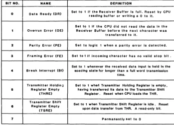
tied to the connector's Received Line Signal Detect (RLSD), allowing RLSD to be available to signals that require the signal. The following table summarizes the connections between the 8250 and the DCE-type connector.
8250
DSR CTS RTS DTR OUT 1
TABLE 4-3
CONNECTOR
DTR RTS CTS DSR RLSD