Room-temperature quantum interference in single
perovskite quantum dot junctions
Haining Zheng
1,4, Songjun Hou
2,4, Chenguang Xin
3,4, Qingqing Wu
2, Feng Jiang
1, Zhibing Tan
1, Xin Zhou
3,
Luchun Lin
1, Wenxiang He
1, Qingmin Li
1, Jueting Zheng
1, Longyi Zhang
1, Junyang Liu
1, Yang Yang
1, Jia Shi
1,
Xiaodan Zhang
3, Ying Zhao
3, Yuelong Li
3*, Colin Lambert
2* & Wenjing Hong
1*
The studies of quantum interference effects through bulk perovskite materials at the Ång-strom scale still remain as a major challenge. Herein, we provide the observation of room-temperature quantum interference effects in metal halide perovskite quantum dots (QDs) using the mechanically controllable break junction technique. Single-QD conductance mea-surements reveal that there are multiple conductance peaks for the CH3NH3PbBr3 and
CH3NH3PbBr2.15Cl0.85QDs, whose displacement distributions match the lattice constant of
QDs, suggesting that the gold electrodes slide through different lattice sites of the QD via Au-halogen coupling. We also observe a distinct conductance ‘jump’ at the end of the sliding process, which is further evidence that quantum interference effects dominate charge transport in these single-QD junctions. This conductance ‘jump’ is also confirmed by our theoretical calculations utilizing density functional theory combined with quantum transport theory. Our measurements and theory create a pathway to exploit quantum interference effects in quantum-controlled perovskite materials.
https://doi.org/10.1038/s41467-019-13389-7 OPEN
1State Key Laboratory of Physical Chemistry of Solid Surfaces, iChEM, NEL, College of Chemistry and Chemical Engineering, Xiamen University, Xiamen
361005, China.2Department of Physics, Lancaster University, Lancaster LA1 4YB, UK.3Institute of Photoelectronic Thin Film Devices and Technology, Key
Laboratory of Photoelectronic Thin Film Devices and Technology of Tianjin, Key Laboratory of Optical Information Science and Technology of Ministry of Education, Nankai University, Tianjin 300350, China.4These authors contributed equally: Haining Zheng, Songjun Hou, Chenguang Xin. *email:lyl@nankai.
edu.cn;[email protected];[email protected]
123456789
Q
uantum interference (QI) effects, originating from de Broglie waves of electrons traversing different pathways through nanoscale junctions, underpin the conceptual designs of molecular devices such as QI based field-effect transistors1,2. Previous experimental and theoretical investiga-tions of room-temperature QI effects have mainly focused on organic molecular wires, including π-conducting wires3, σ -conducting wires4, and evenπ-stacked dimers5, but the exploi-tation of room-temperature QI effects in electron transport through Ångstrom-scale inorganic systems still remains unex-plored. The unique quantum yields and high carrier mobility of perovskite-based electronic materials offer a platform for us to translate knowledge of their macroscopic charge transport into the quantum effects at the nanoscale.Perovskite materials attract extraordinary attention in applica-tions of the light-emitting diode6, photodetector7, and solar cells8,9. Although there are many experimental investigations of charge transport through bulk perovskite materials, including thinfilms10, nanocrystals11, and single crystals12, investigations at the nanoscale, to reveal QI effects in their room-temperature transport properties remain as a major experimental challenge. The extensions of single-molecule charge transport measurements from conjugated mole-cular families13 to molecular assemblies14,15, clusters16, and the recently developed Au-halogen interfacial engineering17 offer an opportunity to gain an insight into microscopic charge transport through Ångstrom-scale perovskite materials.
To understand how their macroscopic charge transport prop-erties lead to quantum effects at the nanoscale, here we report the observation of room-temperature QI effects in metal halide per-ovskite quantum dots (QDs) at the Ångstrom scale using the mechanically controllable break junction (MCBJ) technique combined with quantum transport theory and calculations. Multiple distinguishable conductance peaks can be observed in
the MAPbBr3 and MAPbBr2.15Cl0.85 (MA=CH3NH3+) QDs,
while MAPbBr2.15I0.85, MAPbCl3 and MAPbI3 QDs show no
significant conductance features. The displacement distributions also match well with the lattice constant of QDs, suggesting that the multiple conductance features are derived from the sliding of gold electrodes through different lattice sites of the QD via Au-halogen coupling. A distinct conductance‘jump’is also observed at the end of the sliding process, which is further evidence that QI effects dominate charge transport in the single-QD junctions.
Results
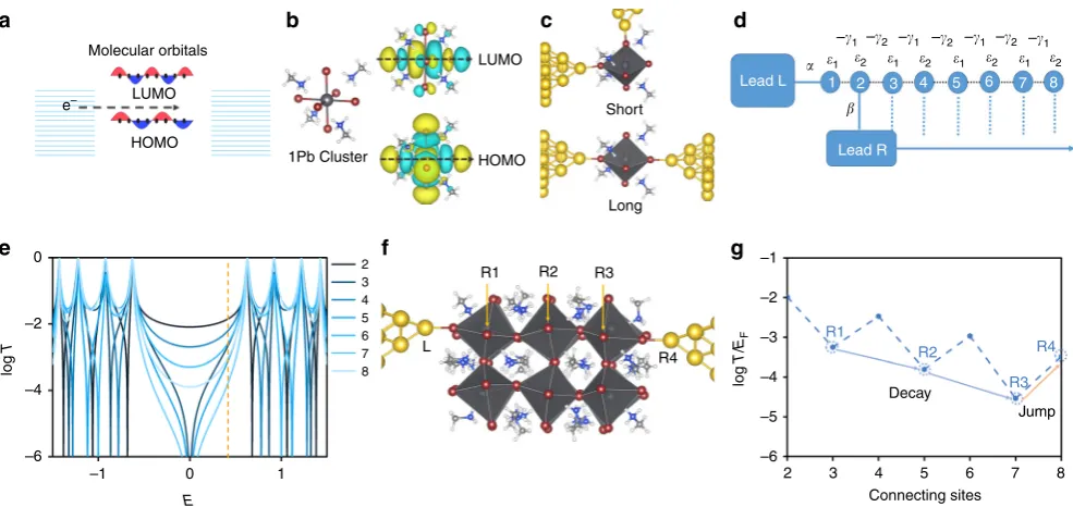
Theory of room-temperature QI effects. The tunneling trans-port through QDs or molecules is mediated by electrons whose energy lies within the energy gap between the highest occupied molecular orbital (HOMO) and lowest occupied molecular orbital (LUMO), thus the inter-orbital QI can be understood qualita-tively by inspecting the signs of the HOMO and LUMO at the points of contact between the molecule and electrode (Fig.1a). As mentioned in previous literature18–20, if the coupling between molecule and electrode is weak, the effect of QI on transport properties could be predicted by examining the Green’s function
G(EF)of the isolated molecule. The transmission amplitude of an
electron with energy EF from site i to j is proportional to
Gi;jð Þ ¼EF
PN
n¼1
ϕn iϕnj
EFεn, whereϕ
n
i is the amplitude ofnthmolecular
orbital (MO) on site i and εnis the corresponding MO energy
level. Taking only the HOMO and LUMO into consideration and assuming that EFis located in the midgap of HOMO and
LUMO, this equation could be further written as Gi;jð Þ EF 1
Δ ϕHOMOi ϕHOMOj ϕLUMOi ϕLUMOj
¼1
ΔðaHaLÞ, whereΔis half
of the gap of HOMO and LUMO, aH¼ϕHOMOi ϕHOMOj ;aL¼
ϕLUMO
i ϕLUMOj . Therefore, constructive quantum interference
a
Molecular orbitals
1Pb Cluster LUMO
HOMO
LUMO
Short
Lead L
Lead R 2
–1
1 2 1 2 1 2 1 2
–1 –1 –1
–2 –2 –2
3 4 5 6 7 8
1
Long
R1 R2
2 3 0
–2
–4
–1 0 1
E
log
T
–6
4 5 6 7 8
R3
L
R4
–1
–2
2 3 4 5
Connecting sites
6 7 8
–3
Decay
R1
R2
R3 R4
Jump –4
–5
–6
log
T
/
EF
HOMO
e–
e f
b c d
g
[image:2.595.51.544.403.636.2](CQI) corresponding to a large value ofjGi;jð ÞjEF is predicted if
aH and aL have opposite signs, while destructive quantum
interference (DQI), corresponding to a low value ofjGi;jð ÞjEF , is
predicted ifaHandaLhave the same sign. As an example of this
sign dependence, if the electrodes make contact with the left and right ends of the perovskite cluster in Fig. 1c, the LUMO has a positive amplitude on the left (yellow) and a negative amplitude on the right (blue), hence the product (aL) is negative.
On the other hand, the HOMO has a positive amplitude on the left and a positive amplitude on the right, hence the product (aH) is positive. Therefore, CQI is expected. Hence when
elec-trodes are attached to the perovskite junctions with ‘long’ or
‘short’sites in Fig.1c, the transmission functions obtained from density functional theory (DFT) calculation reveal counter-intuitively that the conductance of the latter is higher than that of the former over a wide energy range (see Supplementary Fig. 24). The fact that HOMO and LOMO orbital products correspond-ing to contacts at the ends of such molecules are of opposite signs is a consequence of orthogonality. The reason is that orthogon-ality requires that the number of sign changes must differ by unity if the nodal structure of the HOMO and LOMO are the same in the direction transverse to their long axis. Therefore CQI is expected to be a common feature of end-contacted molecules. As shown in Fig.1d, if one electrode is placed at the left end of a molecule (site 1) and the other electrode makes successive contacts along the length of a molecule (L=2, 3, ……8) (the other models are shown in Supplementary Fig. 23), counter-intuitively, the conductance measured at the largest value of L
(site 8) should lie above the trend defined by the tunneling decay equation G~e−βL. The transmission function for this simple
model (Fig.1e) shows that quantum oscillations will occur over a wide range of electron energiesEwithin the HOMO-LUMO gap under these circumstances. To employ this model for the perovskite materials, as indicated in Fig. 1f, a model for contacting perovskite clusters involves successive contacts with odd-numbered sites, followed by a conductance jump at thefinal contact (orange arrow in Fig. 1g). The above analysis suggests that perovskite quantum clusters provide an ideal platform for identifying room-temperature QI transport features at the Ångstrom scale.
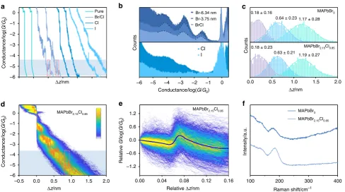
Single-molecule conductance measurements. To explore the QI in perovskite clusters, we experimentally investigate electron transport through single perovskite QD junctions bonded to two gold electrodes through Au-halogen bonds. Four types of organic-inorganic metal halide perovskite QDs MAPbX3 (MA=
CH3NH3+, X=I−, Br-, Cl−, a mixture of Br− and Cl−)
are synthesized with oleic acid and octylamine as ligands to enhance colloidal stability and suppress QD aggregation effects (See Method, Supplementary Figs. 5–6 and Supplementary Note 2–3 for more details)21. As shown in Fig. 2a, the typical ABX3 perovskite-type structure is composed of the framework
of [PbX6]- octahedra occupied by methylammonium cation
(MA+) in the four octahedra central positions. Single-QD con-ductance measurements of MAPbBr3 are carried out using the
MCBJ technique in a solution containing 0.365 mg mL−1
QDs with 1, 3, 5-trimethylbenzene (TMB) as a solvent (see Sup-plementary Figs. 7–8 and Note 4 for more details of the MCBJ measurement)22. As shown in Fig.2b, the individual conductance-distance curves of solvent without QDs show a monotonic
–0.5 0.0 0.5 1.0 1.5 2.0
–6 –5 –4 –3 –2 –1 0
Conductance/log(
G
/
G0
)
Δz/nm
0.00 0.04 0.08 0.12 0.16
-1.4 -0.7 0.0 0.7 1.4
Relative
G
/log(
G
/
G0
)
Relative Δz/nm
–6 –5 –4 –3 –2 –1 0
Conductance/log(
G
/
G0
)
Δz/nm
A
Br–
Br–/Cl–
Cl–
I–
Pb2+
CH3NH3+
d a
c
MAPbBr3 MAPbBr3
b
[image:3.595.120.474.396.671.2]exponential decay after the breaking of gold-gold atomic junctions at conductance quantum G0 (where G0 is the conductance
quantum, which equals 2e2 h−1), while three distinguished
con-ductance plateaus and ‘jump plateaus’ appear in the traces of MAPbBr3. To reveal the source of the conductance plateaus, we
also carry out the MCBJ measurements of all ligands and ingre-dients used in the synthesis of the QDs in the solvent γ -butyr-olactone, including oleic acid, octylamine, PbBr2, PbCl2, MACl,
and MABr. The obvious conductance plateau can be observed in PbBr2, while no clear conductance signal can be observed in
other ligands and raw materials, suggesting that the conductance signal may come from Au–Br interaction and the other ligands cannot form the single-QD junction (Supplementary Fig. 10 and Note 6). We also characterize the bias-voltage dependence of single-QD conductance over the range from 50 to 250 mV (See Supplementary Fig. 11a), which agrees with the Simmons model and suggests that charge transport is mediated by an off-resonant coherent tunneling mechanism. The single-QD junctions become quite unstable at higher bias voltage (300 and 400 mV) and the conductance values of three plateaus are difficult to identify, which may be due to the destruction of the perovskite clusters at such high electricfields (See Supplementary Fig. 12 and Note 8).
To further demonstrate the conductance evolution during the break junction processes, the two-dimensional (2D) conductance-displacement histogram is plotted in Fig.2c, and shows multiple distinct conductance clouds, indicating a high molecular junction formation probability and distinct charge transport properties of each configuration. Interestingly, we observe a clear conductance jump at the end of the third plateau in approximately 70% of the
individual conductance-distance traces of MAPbBr3(See
Supple-mentary Fig. 14 and Note 9 for more analytical details)23. As shown in Fig.2d, a clear jump in conductance could be observed at the relative displacement of approximately 0.05 nm with conductance difference around one order of magnitude, suggest-ing that the ssuggest-ingle-QD junction exhibits higher conductive state at the end of the sliding process of the two gold electrodes on the QDs.
To reveal the binding geometries of the single-QD junctions, we carry out the single-QD conductance measurements of MAPbBr2.15Cl0.85, MAPbBr2.15I0.85, MAPbCl3 and MAPbI3
QDs. Figure 3a shows several individual conductance-distance curves of these three QDs and pure solvent. For MAPbBr2.15Cl0.85, multiple conductance features are also
observed, which are similar to those of MAPbBr3. The
one-dimensional (1D) conductance histograms (Fig. 3b) also show three similar conductance features located at 10–1.54, 10−2.72and
10−4.13G0 for MAPbBr3, 10−1.51, 10−2.81 and 10−4.21G0 for
MAPbBr2.15Cl0.85, respectively, and the conductance evolution
and ‘jump curves’ is also similar with that of MAPbBr3 (see
Fig. 3d, e, Supplementary Fig. 15 and Note 10), suggesting the binding of MAPbBr2.15Cl0.85 also comes from the Au–Br
coordination. We also construct the conductance histograms for MAPbCl3, MAPbI3, and MAPbBr2.15I0.85 from approximately
2500 individual traces (Fig.3b and Supplementary Fig. 16), and no conductance peaks are observed, while the peak of the gold–gold atomic junction atG0for MAPbI3and MAPbBr2.15I0.85
becomes less clear than others. In addition, we also carry out the MCBJ measurements using the MAPbBr3QDs with the average
diameters of 6.34 nm and 3.75 nm, which are obtained from the
–0.5 0.0 0.5 1.0 1.5 2.0
–6 –5 –4 –3 –2 –1 0
Conductance/log(
G
/
G0
)
Δz/nm
0.00 0.04 0.08 0.12 0.16
–1.2 –0.6 0.0 0.6 1.2
Relative
G
/log(
G
/
G0
)
Relative Δz/nm
MAPbBr2.15Cl0.85 Pure
Br/Cl Cl I
–6 –5 –4 –3 –2 –1 0
Conductance/log(
G
/
G0
)
e
1.17 ± 0.28 0.64 ± 0.23 0.18 ± 0.16
0.0 0.5 1.0 1.5 2.0
0.63 ± 0.21
1.19 ± 0.27 0.18 ± 0.23
Δz/nm
Counts
a b c
d f
MAPbBr3
MAPbBr2.15Cl0.85
100 200 300 400
Intensity/a.u.
Raman shift/cm–1
MAPbBr3
MAPbBr2.15Cl0.85 MAPbBr2.15Cl0.85
Br-6.34 nm Br-3.75 nm BrCl
–6 –5 –4 –3 –2 –1 0
Cl I
Counts
Conductance/log(G/G0)
Δz/nm
[image:4.595.55.544.48.320.2]centrifugal speeds of 10000 rpm and 5000 rpm, respectively (as shown in Supplementary Figs. 3 and 17). The experimental results show that the QDs with different diameters show similar conductance features, indicating that the conductance plateaus we measured originate from the perovskite crystal cells rather than the entire perovskite QDs. Furthermore, we calculate the Au-halogen binding energy by using DFT and find that the Au-halogen binding energy is in accordance with the order of Au-I > Au–Br > Au–Cl (See Supplementary Table 3 and Note 16 for more details). The comparison of different QDs suggests that for MAPbCl3QDs, the bond energy of Au–Cl bond is too weak to
form stable Au-QD-Au junctions. In contrast, the strong Au–I bond may break the crystal structure of MAPbBr2.15I0.85 and
MAPbI3 with the sliding process of the electrodes due to the
poorer stability of crystal structure24–26.
To understand the origins of the multiple conductance features, we analyze the relative displacement distribution of MAPbBr3 and MAPbBr2.15Cl0.85 QDs (The detailed analysis of
how to obtain the displacement distribution is discussed in Supplementary Fig. 9 and Note 5). As shown in Fig. 3c, for MAPbBr3 QDs, the most probable displacements of each
conductance features are 0.18 ± 0.16 nm, 0.64 ± 0.23 nm and 1.17 ± 0.28 nm, while the displacements are 0.18 ± 0.23 nm, 0.63 ± 0.21 nm and 1.19 ± 0.27 nm for MAPbBr2.15Cl0.85QDs,
respec-tively. The average displacement differences are determined to be approximately 0.5 nm from the difference of the above values, which are quite similar for both QDs. The difference of adjacent statistical lengths is approximately consistent with the adjacent lattice distance of Br, confirming that it is the Au–Br coordination that provides the binding sites for Au-QD-Au junctions, during the sliding of gold electrode across the QD’s surface. Charge transport investigation of halogen-terminated single-molecule
oligothiophene junctions also suggested that Au-halogen inter-action could act as a robust anchoring group for binding the molecules to the gold electrodes17. As for the other atoms, the MA+is located at the center of the regular octahedron, which is not easy to connect to the gold electrodes, and the adjacent distance of the MA+is not in accordance with the displacement distributions. The electronegativity of the Pb2+ is low, and the
Pb2+ is hidden within the Br networks that could not have reliable interaction with the gold electrodes. Therefore, the gold electrodes interact with halogen, rather than other atoms or groups, to form stable Au-QD-Au junctions. To provide direct evidence of the Au–Br bond, we further perform the shell-isolated nanoparticle-enhanced Raman spectroscopy (SHINERS). As shown in Fig. 3f, two distinct Raman peaks can be observed at approximately 180 cm−1 for MAPbBr3 and MAPbBr2.15Cl0.85,
which confirms the formation of Au–Br bond27,28, (experimental details are shown in Supplementary Note 11) suggesting the multiple conductance features originate from the sliding of gold electrodes on the surface of single MAPbBr3 and
MAPbBr2.15Cl0.85QD via the Au–Br bond.
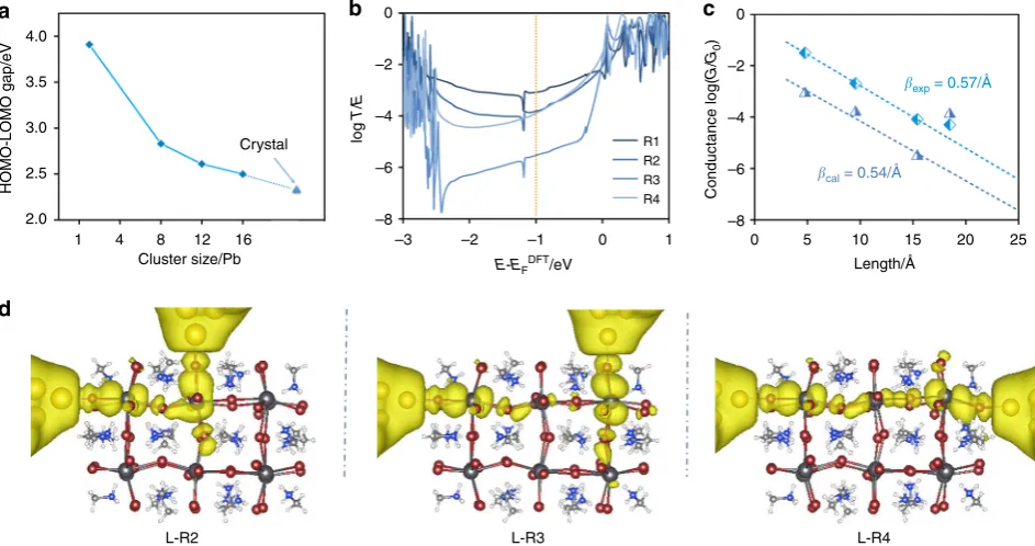
DFT calculation. To gain further insight into the conductance trends observed in the MCBJ measurements, transmission spectra T(E) are calculated by combining the DFT package SIESTA29 with the quantum transport code Gollum30 (see Method for further details). The MAPbBr3 neutral charge
clusters (1Pb (MA4PbBr6), 8Pb (MA20Pb8Br36), 12Pb
(MA28Pb12Br52), 16Pb (MA36Pb16Br68)) are built with the same
method as the literature31(see Supplementary Fig. 25). For the crystal MAPbBr3, our calculated band gap of 2.31 eV agrees well
with the experimental value 2.24 eV (Fig.4a)32, along with the
a b c
d
4.0
3.5
3.0
2.5
2.0
1 4 8 12 16
–2
R1 R2 R3 R4 0
–4
–6
–8
–3 –2 –1
E-EFDFT/eV
0 1
–2 0
–4
0 5 10
Length/Å 15 exp = 0.57/Å
cal = 0.54/Å
20 25
–6
–8
Cluster size/Pb
L-R2 L-R3 L-R4
Crystal
HOMO-LOMO gap/eV
log
T
/
E
Conductance log(
G
/
G0
)
Fig. 4The charge transport property of 12Pb MAPbBr3with different connectivities.aHOMO-LUMO gaps with respect to the size of MAPbBr3clusters.
bThe transmission spectra of different connectivities as the function ofEEDFT
[image:5.595.62.534.417.666.2]HOMO-LUMO gaps of MAPbBr3clusters of different sizes. As
the size of the clusters decreases, their HOMO-LUMO gaps increase to 2.5 eV (for 16Pb) and further to 3.91 eV (for 1Pb) due to the stronger quantum confinement effect. After the rupture of the gold wire, the initial gap width is known to be a snap-back distance of about 5 Å. Since this corresponds to the distance between two neighboring Br atoms (around 5 Å), these two Br atoms are most likely to be connected to the gold atoms at the beginning in this sliding process. As for the sliding direction, the gold electrode could slide from the top of one Br atom to its adjacent Br atom along the horizontal and diagonal directions (shown as green and red arrows in Supplementary Fig. 30). The corresponding total energies upon sliding along one unit cell are shown in Supplementary Fig. 30c. Compared with displacement along the green ‘horizontal’ direction, the energy barrier is much higher in the red‘diagonal’direction due to the existence of CH3NH3+in the cavity. This demonstrates
that there is a low-energy channel for sliding along the ‘ hor-izontal’ direction, whereas the ‘diagonal’ direction contains a high-energy barrier and is less likely to happen in a real experiment. In order to further analyze the possible binding sites of the gold electrodes during the sliding process, we use the spectral clustering algorithm to give comprehensive and detailed classifications of the individual conductance-distance traces. The original conductance-distance traces can mainly be divided into five categories (as shown in Supplementary Figs. 20–22 and Note 5). The results show that although the three-step plateaus do not always appear simultaneously, the classified conductance plateaus display similar conductance features, i.e. the similar conductance values and displacement distributions, further confirming that the gold electrodes are more likely to slide along the‘horizontal’direction rather than the ‘diagonal’direction. Therefore, the sliding along the ‘ hor-izontal’ direction is adopted here to understand what we observed experimentally.
In the current study, the fully relaxed 12Pb MAPbBr3cluster
is connected to two gold electrodes through two Br atoms as shown in Fig.1f, where the Br atom labeled by‘L’is attached to the left gold electrode, the right gold electrode is attached successively to Br atoms labeled by‘R1’,‘R2’,‘R3’, and‘R4’to model a sliding process. The corresponding transmission spectra are plotted in Fig. 4b. When the Fermi energy lies within the HOMO-LUMO gap, charge transfer occurs through the junction via off-resonant tunneling and the tunneling probability decays exponentially with L. Therefore, we fit the room-temperature conductance (EF=−1.0 eV) to an
expo-nential function, which led to an attenuation factor ofβ=0.54 Å−1was obtained, which is consistent with our measured value
of 0.57 Å−1, as shown in Fig. 4c. More interestingly, in
agreement with our experiments, when the right electrode is moved from ‘R3’ to the furthest distance ‘R4’, we obtain a much higher conductance compared with the shorter path‘R3’. This increase is also reflected in the qualitative behavior of the local density of states (LDOS) for ‘L-R2’, ‘L-R3’, and ‘L-R4’ (Fig. 4d). In contrast with R3, the weights of LDOS extend almost continuously between the left electrode and R4. This increase at the most distant electrode separation is also found in 8Pb, 10Pb (obtained by removing two Pb units based on the 2 × 2 × 3 12Pb MAPbBr3), 16Pb and 18Pb MAPbBr3 clusters
(Supplementary Figs. 26–31 and Supplementary Figs. 36–37). Other possible connectivities for 16Pb MAPbBr3 cluster are
also explored (Supplementary Fig. 27–28). We find that this jump behavior is generic although different β factors are observed (0.72 and 1.2 Å−1 separately), and the latter
connectivity is less likely to appear in the experiments due to the higher energy barrier.
The influence of ligand (oleic acid and octylamine) on the transmission functions is investigated by considering the ligands staying close to the cluster or bridging the gold electrode and perovskite cluster (see Supplementary Figs. 32 and 33). Our results reveal that the effect of ligand is negligible due to the weak coupling between ligands and cluster or gold electrode. We also carry out DFT calculations for MAPbCl3and MAPbI3QDs. Our
results show that the three halide perovskite QDs possess similar charge transport features (see Supplementary Figs. 34 and 35). However, as mentioned above, in a real experiment they are not expected to form junctions, because of the weaker Au–Cl bond and the poorer stability of crystal structure for MAPbI3QDs24–26.
Two new left binding sites (Laand Lb) are also considered in our
calculations. As shown in Supplementary Figs. 38 and 39, wefind the conductance evolution follows the same trend as the binding sites of L, i.e. itfirst decays exponentially and then jumps at the end. However, the magnitude of conductances is much smaller in these two cases due to the higher barrier caused by the larger Br–Br distance.
Discussion
In summary, we have presented an experimental and theoretical investigation of room-temperature QI effects in the electron transport through single perovskite QD junctions, using a com-bination of DFT and the MCBJ technique. Three distinct con-ductance features are observed from the conductance measurements of perovskite QDs with Br, while the QDs with I and Cl show no significant features. The analysis of conductance trends with displacement reveals that the multiple conductance features are derived from the sliding of gold electrodes between the adjacent Br atoms in different unit cells. Counterintuitively, we also observe a distinct conductance ‘jump’ at the end of individual conductance traces, which is direct evidence of the room-temperature QI effects. This work offers an insight into QI effects in perovskite materials at the single-unit-cell level and also provides an opportunity to explore a strategy for optimizing electron transport in perovskite QDs electronic and optoelec-tronic devices.
Method
Synthesis of MAPbX3(MA=CH3NH3+,X=I−, Br−, Cl−, a mixture of Br−and
Cl−) perovskite QDs. Perovskite QDs in this paper are synthesized according to published papers21. Typically, 0.2 mmol PbBr2(or PbCl2for MAPbCl3, and PbI2 for MAPbI3) and 0.16 mmol MABr (or MACl for MAPbCl3and MAPbBr2.15Cl0.85,
MAI for MAPbI3and MAPbBr2.15I0.85) is dissolved in 5 mL DMF. 0.5 mL oleic acid
and 20μLn-octylamine are added to obtain a stable precursor solution. The 1 mL precursor solution is rapidly injected into 5 mL toluene under the stirring with 800 rpm. In the stirring process, strong green PL emission from MAPbBr3QDs can be
observed under normal room light without using additional excitation light source. Then the precursor solution is centrifugated at 5000 or 10,000 rpm for 10 min to discard the precipitates.
Characterization. Transmission electron microscopy (TEM) and high-resolution TEM (HRTEM): a drop of diluted QDs solution is spread onto an ultrathin carbon
film-coated copper grid and is further dried by gentle N2blowing. Transmission
electron microscopy (TEM, JEOL JEM-2000EX) with fast operation at 200 kV is employed to obtain TEM or HRTEM images before damaging perovskite QDs.
conductance-distance traces of the single-QD junctions can be collected and further analyze the most probable conductance of the junctions.
DFT theoretical calculation. Using the DFT code SIESTA29geometrical opti-mizations were carried out until all the forces were less than 0.05 eV Å−1. A generalized gradient approximation functional (GGA), a double-ζbasis for Au, a double-ζpolarized basis for other elements and a real grid cutoff energy of 150 Ry were employed29,30. A scalar relativistic norm-conserving pseudopotential is used to describe Pb. To compute their electrical conductance, the molecules are each placed between pyramidal gold electrodes. After relaxation, the optimized separation between contact halogen atoms (Cl, Br, I) and apex gold atom was found to be 2.66 Å, 2.76 Å and 2.88 Å, respectively. From the converged DFT calculation of each structure, the meanfield Hamiltonian and overlap matrix are extracted, which are utilized to calculate the transmission coefficientT(E) using the Gollum code30, via the expression
T Eð Þ ¼TrΓLð ÞGE rð ÞEΓRð ÞGE yrð ÞE
: ð1Þ
In this equation,ΓL;Rð Þ ¼E iðΣL;Rð Þ E ΣyL;RðEÞÞ=2.ΓL,Rdescribes the level
broadening due to the interaction between left (right) electrodes and the scattering region.ΣL;Rð ÞE are the self-energies.Gr¼ðESHΣLΣRÞ1is the retarded
Green’s function, whereSandHare the Hamiltonian and overlap matrix, respectively. The room-temperature conductance is obtained by the following formula:G¼G0
Rþ1
1dETðEÞð∂f∂ðEEÞÞ, whereG0=2e2h−1is the conductance
quantum;his the Planck’s constant;eis the charge of a proton; fð Þ ¼E ð1þexpððEEFÞ=kBTÞÞ1is the Fermi–Dirac probability distribution function,
EFis the Fermi energy.
Reporting summary. Further information on research design is available in the Nature Research Reporting Summary linked to this article.
Data availability
The source data underlying Fig. 1e, Fig. 1g, Fig. 2b-d, Fig. 3a-f and Fig. 4a-c are provided as a Source Datafile. All other data are available from the corresponding author upon reasonable requests.
Code availability
The source code of the algorithms are available for research uses athttps://github.com/ zhenghaining121/QDs-codes. Computational data used to arrive at the conclusions presented in the manuscript are available upon reasonable request.
Received: 20 June 2019; Accepted: 6 November 2019;
References
1. Li, Y. et al. Gate controlling of quantum interference and direct observation of anti-resonances in single molecule charge transport.Nat. Mater.18, 357–363 (2019).
2. Bai, J. et al. Anti-resonance features of destructive quantum interference in single-molecule thiophene junctions achieved by electrochemical gating.Nat.
Mater.18, 364–369 (2019).
3. Guédon, C. M. et al. Observation of quantum interference in molecular charge transport.Nat. Nanotechnol.7, 305–309 (2012).
4. Garner, M. H. et al. Comprehensive suppression of single-molecule conductance using destructiveσ-interference.Nature558, 415–419 (2018).
5. Frisenda, R., Janssen, V. A., Grozema, F. C., van der Zant, H. S. & Renaud, N. Mechanically controlled quantum interference in individualπ-stacked dimers.
Nat. Chem.8, 1099–1104 (2016).
6. Tan, Z.-K. et al. Bright light-emitting diodes based on organometal halide perovskite.Nat. Nanotechnol.9, 687–692 (2014).
7. Lin, Y., Lin, G., Sun, B. & Guo, X. Nanocrystalline perovskite hybrid photodetectors with high performance in almost everyfigure of merit.Adv.
Funct. Mater.28, 1705589 (2018).
8. Zhou, H. et al. Interface engineering of highly efficient perovskite solar cells.
Science345, 542–546 (2014).
9. Im, J.-H., Jang, I.-H., Pellet, N., Grätzel, M. & Park, N.-G. Growth of CH3NH3PbI3cuboids with controlled size for high-efficiency perovskite solar
cells.Nat. Nanotechnol.9, 927–923 (2014).
10. Liu, M., Johnston, M. B. & Snaith, H. J. Efficient planar heterojunction perovskite solar cells by vapour deposition.Nature501, 395–398 (2013). 11. Malgras, V. et al. Observation of quantum confinement in monodisperse
methylammonium lead halide perovskite nanocrystals embedded in mesoporous silica.J. Am. Chem. Soc.138, 13874–13881 (2016).
12. Shi, D. et al. Low trap-state density and long carrier diffusion in organolead trihalide perovskite single crystals.Science347, 519–522 (2015).
13. Leary, E. et al. Incorporating single molecules into electrical circuits. The role of the chemical anchoring group.Chem. Soc. Rev.44, 920–942 (2015). 14. Famili, M. et al. Self-assembled molecular-electronicfilms controlled by room
temperature quantum interference.Chem5, 474–484 (2019).
15. Chen, X. et al. Molecular diodes with rectification ratios exceeding 10 5 driven by electrostatic interactions.Nat. Nanotechnol.12, 797–803 (2017). 16. Lovat, G. et al. Room-temperature current blockade in atomically defined
single-cluster junctions.Nat. Nanotechnol.12, 1050–1054 (2017).
17. Xiang, L. et al. Non-exponential length dependence of conductance in iodide-terminated oligothiophene single-molecule tunneling junctions.J. Am. Chem. Soc.138, 679–687 (2016).
18. Lambert, C. J. & Liu, S. X. A magic ratio rule for beginners: a chemist’s guide to quantum interference in molecules.Chem.—Eur. J.24, 4193–4201 (2018). 19. Zhao, X., Geskin, V. & Stadler, R. Destructive quantum interference in
electron transport: A reconciliation of the molecular orbital and the atomic orbital perspective.J. Chem. Phys.146, 092308 (2017).
20. Yoshizawa, K. An orbital rule for electron transport in molecules.Acc. Chem. Res.45, 1612–1621 (2012).
21. Zhang, F. et al. Brightly luminescent and color-tunable colloidal
CH3NH3PbX3(X=Br, I, Cl) quantum dots: potential alternatives for display
technology.ACS nano9, 4533–4542 (2015).
22. Liu, J. et al. Transition from tunneling leakage current to molecular tunneling in single-molecule junctions.Chem5, 390–401 (2019).
23. Frei, M., Aradhya, S. V., Koentopp, M., Hybertsen, M. S. & Venkataraman, L. Mechanics and chemistry: single molecule bond rupture forces correlate with molecular backbone structure.Nano Lett.11, 1518–1523 (2011).
24. Faghihnasiri, M., Izadifard, M. & Ghazi, M. E. DFT study of mechanical properties and stability of cubic methylammonium lead halide perovskites (CH3NH3PbX3,X=I, Br, Cl).J. Phys. Chem. C.121, 27059–27070 (2017).
25. Rakita, Y., Cohen, S. R., Kedem, N. K., Hodes, G. & Cahen, D. Mechanical properties ofAPbX3(A=Cs or CH3NH3;X=I or Br) perovskite single
crystals.MRS Commun.5, 623–629 (2015).
26. Dong, X. et al. Improvement of the humidity stability of organic–inorganic perovskite solar cells using ultrathin Al2O3 layers prepared by atomic layer deposition.J. Mater. Chem. A3, 5360–5367 (2015).
27. Li, J. F. et al. Shell-isolated nanoparticle-enhanced Raman spectroscopy.
Nature464, 392–395 (2010).
28. Lin, H.-X. et al. Constructing two-dimensional nanoparticle arrays on layered materials inspired by atomic epitaxial growth.J. Am. Chem. Soc.137, 2828–2831 (2015).
29. Soler, J. M. et al. The SIESTA method for ab initio order-N materials simulation.J. Phys.: Condens. Matter14, 2745–2779 (2002).
30. Ferrer, J. et al. GOLLUM: a next-generation simulation tool for electron, thermal and spin transport.New J. Phys.16, 093029 (2014).
31. Giorgi, G., Yoshihara, T. & Yamashita, K. Structural and electronic features of small hybrid organic–inorganic halide perovskite clusters: a theoretical analysis.Phys. Chem. Chem. Phys.18, 27124–27132 (2016).
32. Liu, Y. et al. Two-inch-sized perovskite CH3NH3PbX3(X=Cl, Br, I) crystals:
growth and characterization.Adv. Mater.27, 5176–5183 (2015).
Acknowledgements
This work was supported by the National Key R&D Program of China
(2017YFA0204902, 2014DFE60170, 2018YFB1500105), the National Natural Science Foundation of China (Nos. 21673195, 21503179, 21490573, 61674084, 61874167), the Open Fund of the Key Laboratory of Optical Information Science & Technology (Nankai University) of China, the Fundamental Research Funds for the Central Universities of China (63181321, 63191414, 96173224), and the 111 Project (B16027), the Tianjin Natural Science Foundation (17JCYBJC41400), FET Open project 767187—QuIET, the EU project BAC-TO-FUEL and the UK EPSRC projects EP/N017188/1, EP/M014452/1.
Author contributions
W.H., C.L., and Y.L. designed the experiments and co-supervised the project. H.Z. and S. H. wrote the manuscript with inputs from all authors. H.Z., Z.T., F.J., J.Z., J.P., W.H., Q. L., and J.L. carried out the break junction experiments and analyzed the data. L.L. provided the spectral clustering algorithm for the classifications of the individual conductance-distance traces. C.X., X.Z., Y.L., X.Z., and Y.Z. were responsible for mole-cular synthesis and characterization. J.S., L.Z., and Y.Y. built the electrical measurement instrument and wrote the software to control the break junction setup. C.L., S.H. and Q. W. developed the underlying theoretical concepts. All authors conceived the work and discussed the experiments.
Competing interests
Additional information
Supplementary informationis available for this paper at https://doi.org/10.1038/s41467-019-13389-7.
Correspondenceand requests for materials should be addressed to Y.L., C.L. or W.H.
Peer review informationNature Communicationsthanks Limin Xiang and the other, anonymous, reviewer(s) for their contribution to the peer review of this work. Peer reviewer reports are available.
Reprints and permission informationis available athttp://www.nature.com/reprints
Publisher’s noteSpringer Nature remains neutral with regard to jurisdictional claims in published maps and institutional affiliations.
Open Access This article is licensed under a Creative Commons Attribution 4.0 International License, which permits use, sharing, adaptation, distribution and reproduction in any medium or format, as long as you give appropriate credit to the original author(s) and the source, provide a link to the Creative Commons license, and indicate if changes were made. The images or other third party material in this article are included in the article’s Creative Commons license, unless indicated otherwise in a credit line to the material. If material is not included in the article’s Creative Commons license and your intended use is not permitted by statutory regulation or exceeds the permitted use, you will need to obtain permission directly from the copyright holder. To view a copy of this license, visithttp://creativecommons.org/ licenses/by/4.0/.