Microchip lasers
310
0
0
Full text
(2) Declarations. I, Richard Conroy, hereby certify that this thesis, which is approximately 77000 words in length, has been written by me, that it is a record of work carried out by me and that it has not been submitted in any previous application for a higher degree. I was admitted as a research student in October 1994 and as a candidate for the degree of Doctor of Philosophy; the higher study for which this is a record was carried out in University of St. Andrews between 1994 and 1998. In submitting this thesis to the University of St. Andrews I understand that I am giving permission for it to be made available for use in accordance with the regulations of the University Library for the time being in force, subject to any copyright vested in the work not being affected thereby. I also understand that the title and abstract will be published, and that a copy of the work may be made and supplied to any bona fide library or research worker.. Richard Conroy. 28 August, 2008. I hereby certify that the candidate has fulfilled the conditions of the Resolutions and Regulations appropriate for the degree of Doctor of Philosophy in the University of St. Andrews and that the candidate is qualified to submit this thesis in application for that degree.. Dr Bruce Sinclair. 28 August, 2008. i.
(3) Acknowledgements 'Not everything in black & white makes sense' - Guinness Advert. This thesis has only been made possible by the contributions and support of a large number of people. I am especially indebted to Bruce for his support, guidance and enthusiasm over the last four years. I had great pleasure working with Neil and Dave over the first two years of this work, both teaching me a lot, some of which is perhaps better not knowing! More recently Alan and Graham have taken the group in new directions, including underwater, and I have thoroughly enjoyed the experience of working with them. Much of the content of this thesis has been aided by these four, and on a day-to-day basis they provided an excellent group in which to work, and I owe them a big vote of thanks. Over the years we also saw a number of other people come and go from the group, mainly honours degree project students. James, Tanya, Liese and Alex all provided a welcome diversion and made a significant contribution to the work recorded here and I am very grateful to them for their enthusiasm and hard work. My refuge of Regs was a great place to adjust back to normality. A large number of people, especially Kate and Ian, helped in showing there was more to life than an office with no windows and kept me (reasonably?) sane during the last four years. Finally, I am indebted to my family for supporting and encouraging me through the last eight years, and perhaps, who knows, I may be able to get a 'proper' job now!. ii.
(4) Abstract This thesis is concerned with the characterisation of sub-millimetre sized solid-state lasers. These 'microchip' lasers are examined in two forms; one as monolithic devices where the dielectric mirrors forming the laser cavity are directly deposited onto two near parallel faces of the laser gain crystal, and the second where the microchip gain material is used in combination with a nonlinear crystal to form a composite device. A range of neodymium doped crystals, operating continuous wave and in gainswitched mode at 1064nm, are compared as potential microchip laser gain materials, including Nd:YVO4, Nd:YOS, Nd:SFAP and Nd:SVAP. With the exception of Nd:SVAP, slope efficiencies exceeding 40% and thresholds of less than 100mW were measured for all these lasers. A comparison of the 1064nm and 1342nm transitions in Nd:YVO4 is also carried out showing similar performance for both transitions. The formation of the cavity within these monolithic lasers is described in detail, in particular for the thermal and gain guiding effects in Nd:YVO4. Both analytical and numerical modelling of these effects are compared with experimental measurement of the cavity formation. When used in conjunction with a saturable absorber, these sub-millimetre sized lasers can be used to produce short, high intensity pulses. This is demonstrated using Cr:YAG as a saturable absorber for Nd:YVO4 at 1064nm to produce pulses as short as 1.38ns and peak powers of up to 1kW, and V:YAG to Q-switch Nd:YVO4 at 1342nm to produce pulses with durations as short as 9.5ns and peak powers up to 360W. Active control for generating pulses is also demonstrated using a novel range of deflective Q-switches. These low cost, low loss, compact devices produced pulses of up to 12kW peak power and pulses durations of less than 1.1ns on demand. The continuous wave, intracavity frequency doubling of the three main Nd3+ transitions, to give red, green and blue light is described. Up to 220mW of green light, with an efficiency approaching 40%, 33mW of blue light and 10mW of singlefrequency red light were produced.. iii.
(5) Glossary of Acronyms Crystals Laser Crystals LNP (LiNdP4O12) - lithium neodymium tetraphosphate Nd:LSB (Nd:LaSc3(BO3)4) - lanthanum scandoborate doped with triply ionised neodymium Nd:SFAP (Nd:Sr5(PO4)3F) - strontium fluorophosphate doped with triply ionised neodymium Nd:SVAP (Nd:Sr5(VO4)3F) - strontium fluorovanadate doped with triply ionised neodymium Nd:YAG (Nd:YAl2O3) - yttrium aluminium garnet doped with triply ionised neodymium Nd:YLF - yttrium lithium fluoride doped with triply ionised neodymium Nd:YOS (Nd:Y2SiO5) - yttrium orthosilicate doped with triply ionised neodymium Nd:YVO4 - yttrium orthovanadate doped with triply ionised neodymium Nonlinear Crystals BBO (BaB2O4) - beta-barium borate KNbO3 - potassium niobate KTP (KTiOPO4) - potassium titanyl phosphate LBO (LiB3O5) - lithium triborate LiNbO3 - lithium niobate LiTaO3 - lithium tantalate PPLN - periodically-poled lithium niobate. Laser Characterisation AR - anti-reflecting CCD - charge coupled device CPM - critical phase matching CW - continuous wave DPSSL - diode-pumped solid-state laser DRO - doubly resonant oscillator ESA - excited state absorption FWHM - full width, half maximum GSA - ground state absorption. iv.
(6) HR - highly reflecting MISER - monolithic isolated single-mode end-pumped ring MOCVD - metal-organic chemical vapour deposition MOPA - master oscillator power amplifier MQW - multiple quantum well NCPM - non-critical phase matching OPA - optical parametric amplifier OPD - optical path difference OPO - optical parametric oscillator OSA - optical spectrum analyser Q-Switching - 'quality' switching alters the ratio of the energy stored to the loss of a laser cavity. Can be either passive or active QPD - quadrupole deflector QPM - quasi phase-matching ( )%R - reflectivity of a dielectric coating SEL - surface emitting laser SESAM - semiconductor saturable absorbing mirror SHG - second harmonic generation SLM - single longitudinal mode SQW-SCH - single quantum well, separate confinement heterostructure structure ( )%T - transmission of a dielectric coating TEM00 - transverse electro-magnetic mode with no dark regions in both the vertical and horizontal planes. This is a diffraction limited transverse mode with a single intensity lobe TIR - total internal reflection VCSEL - vertical surface cavity emitting laser. v.
(7) C. Table of Contents. CHAPTER 1 - OVERVIEW OF DIODE-PUMPED SOLID-STATE LASERS (DPSSLS).......... 1 1.1 INTRODUCTION ............................................................................................................................. 1 1.1.1 Background ......................................................................................................................... 2 1.2 HISTORICAL DEVELOPMENT OF DPSSLS ..................................................................................... 3 1.2.1 Realisation of The Laser...................................................................................................... 3 1.2.2 Development of Laser Diodes as Pump Sources ................................................................. 4 1.2.3 Modern Laser Diode Development...................................................................................... 7 1.2.4 Historical Development of Diode Pumped Solid-State Lasers.......................................... 12 1.3 SOLID-STATE LASER MATERIALS ............................................................................................... 19 1.3.1 Vibronic Laser Materials (Transition Metal Ions) ............................................................ 20 1.3.2 Rare-Earth-Ion Doped Materials ...................................................................................... 22 1.3.3 Classification of Host Matrices ......................................................................................... 27 1.4 THE FUTURE OF DPSSLS ........................................................................................................... 29 CHAPTER 2 - DIODE-PUMPING OF MONOLITHIC ND3+ MICROCHIP LASERS ............ 39 2.1 INTRODUCTION ........................................................................................................................... 39 2.2 MATERIAL CHARACTERISATION ................................................................................................. 40 2.2.1 Introduction ....................................................................................................................... 40 2.2.2 Absorption Characteristics................................................................................................ 46 2.2.3 Fluorescence Characteristics ............................................................................................ 47 2.3 LASING CHARACTERISTICS ......................................................................................................... 49 2.3.1 Comparison of Lasing Performance of Nd3+ Doped Materials......................................... 49 2.3.2 Monolithic 1064nm Nd:YVO4 Microchip Lasers............................................................... 52 2.3.3 Monolithic 1342nm Nd:YVO4 Microchip Lasers............................................................... 55 2.3.4 Summary of CW Lasing Performance ............................................................................... 58 2.4 INTENSITY MODULATION OF MONOLITHIC MICROCHIP LASERS ................................................. 59 2.4.1 Introduction ....................................................................................................................... 59 2.4.2 Gain Switching Theory ...................................................................................................... 60 2.4.3 Gain Switching of Nd3+ Doped Monolithic Microchip Lasers .......................................... 65 2.4.4 Repetitive Gain-Switching ................................................................................................. 70 2.5 FREQUENCY MODULATION AND TUNING.................................................................................... 71 2.5.1 Pump Power Frequency Tuning ........................................................................................ 72 2.5.2 Mechanical Tuning............................................................................................................ 75 2.5.3 Electrical Modulation........................................................................................................ 76 2.6 SUMMARY & CONCLUSIONS ....................................................................................................... 77. vi.
(8) CHAPTER 3 - TRANSVERSE MODE DEFINITION IN MICROCHIP LASERS ................... 82 3.1 INTRODUCTION ........................................................................................................................... 82 3.1.1 Behaviour at High Pump Powers ...................................................................................... 83 3.1.2 Cavity Stability .................................................................................................................. 84 3.2 THERMAL MODELLING OF MICROCHIP LASERS .......................................................................... 86 3.2.1 Introduction ....................................................................................................................... 86 3.2.2 Standard Heat Equation .................................................................................................... 92 3.2.3 Parabolic Temperature Profile in Pumped Region ........................................................... 93 3.2.4 Logarithmic Temperature Profile Outside Pumped Region .............................................. 96 3.2.5 Minimum Beam Waist and Pump Power Dependence ...................................................... 97 3.2.6 1-D Analytical Solution to Standard Heat Equation ....................................................... 100 3.2.7 Results of Analytical Models ........................................................................................... 109 3.2.8 Numerical Solutions to the Standard Heat Equation ...................................................... 115 3.3 MEASUREMENT OF OPTICAL DISTORTION ................................................................................ 123 3.3.1 Far-Field Measurement of Optical Distortion ................................................................ 123 3.3.2 Interferometric Measurement of Optical Distortion........................................................ 127 3.3.3 Comparison of Measurement Techniques ....................................................................... 131 3.3.4 Comparison of Theoretical and Experimental Results .................................................... 132 3.3.5 Surface Distortion ........................................................................................................... 133 3.4 GAIN-GUIDING OF TRANSVERSE MODES .................................................................................. 135 3.4.1 Introduction ..................................................................................................................... 135 3.4.2 Experimental Evidence of Gain-Guiding......................................................................... 136 3.4.3 Self Q-Switching in Monolithic Nd:YVO4 Microchip Lasers........................................... 142 3.4.4 Modelling of Gain Guiding ............................................................................................. 149 3.4.5 Gain-Induced Self Q-Switching ....................................................................................... 153 3.5 CONCLUSIONS AND FUTURE WORK .......................................................................................... 155 CHAPTER 4 – Q-SWITCHED MICROCHIP LASERS ............................................................. 159 4.1 INTRODUCTION ......................................................................................................................... 159 4.2 ACTIVE Q-SWITCHING OF MICROCHIP LASERS......................................................................... 162 4.2.1 Introduction ..................................................................................................................... 162 4.2.2 Laser Rate Equations ...................................................................................................... 164 4.2.3 Electro-Optic Deflection.................................................................................................. 170 4.3 PASSIVE Q-SWITCHING OF MICROCHIP LASERS ....................................................................... 185 4.3.1 Introduction ..................................................................................................................... 185 4.3.2 Analytical Modelling of Passive Q-Switching ................................................................. 190 4.3.3 Cr:YAG Passive Q-Switches............................................................................................ 198 4.3.4 V:YAG Passive Q-Switches ............................................................................................. 208 4.4 CONCLUSIONS .......................................................................................................................... 214. vii.
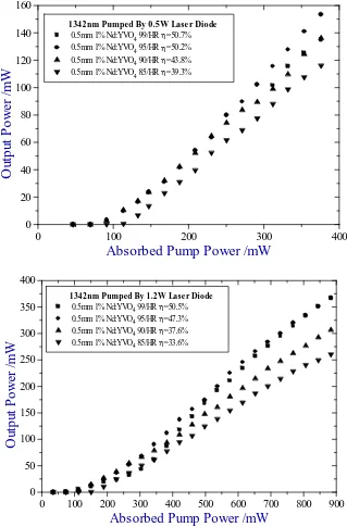
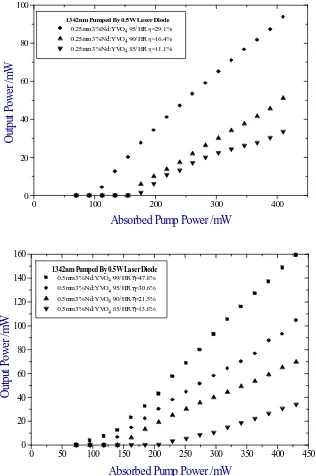
(9) CHAPTER 5 - CW INTRACAVITY FREQUENCY DOUBLING OF ND3+ TRANSITIONS 218 5.1 INTRODUCTION ......................................................................................................................... 218 5.2 FREQUENCY CONVERSION ........................................................................................................ 219 5.2.1 Introduction to Frequency Conversion............................................................................ 219 5.2.2 Frequency Doubling........................................................................................................ 221 5.2.3 Phase Matching Schemes ................................................................................................ 222 5.3 FREQUENCY DOUBLING............................................................................................................ 226 5.3.1 Single-Pass Frequency Doubling .................................................................................... 226 5.3.2 Resonance Cavity Frequency Doubling .......................................................................... 226 5.3.3 Intracavity Frequency Doubling ..................................................................................... 228 5.3.4 Conclusion....................................................................................................................... 234 5.4 INTRACAVITY FREQUENCY DOUBLED MICROCHIP LASERS ...................................................... 235 5.5 INTRACAVITY DOUBLING OF 1064NM TRANSITION IN ND:YVO4 ............................................. 245 5.5.1 Introduction and Motivation............................................................................................ 245 5.5.2 CW Lasing Performance ................................................................................................. 247 5.5.3 Longitudinal Mode Structure........................................................................................... 249 5.5.4 ‘Green Noise’ .................................................................................................................. 250 5.5.5 Long Term Intensity Stability .......................................................................................... 252 5.5.6 Optical Bistability in Green Microchip Lasers................................................................ 253 5.5.7 Microchip Pumped OPO ................................................................................................. 253 5.5.8 Conclusion....................................................................................................................... 255 5.6 INTRACAVITY DOUBLING OF 946NM TRANSITION IN ND:YAG ................................................ 257 5.6.1 Introduction and Motivation............................................................................................ 257 5.6.2 First Blue Microchip Laser ............................................................................................. 258 5.6.3 Second Blue Microchip Laser.......................................................................................... 263 5.6.4 Conclusion....................................................................................................................... 267 5.7 INTRACAVITY DOUBLING OF 1342NM TRANSITION IN ND:YVO4 ............................................. 268 5.7.1 Introduction and Motivation............................................................................................ 268 5.7.2 CW Lasing Performance ................................................................................................. 269 5.7.3 Temperature Bandwidth of LBO...................................................................................... 271 5.7.4 Temperature Tuning and Longitudinal Mode Structure.................................................. 273 5.7.5 ‘Red Noise’ ...................................................................................................................... 275 5.7.6 Long Term Intensity Stability .......................................................................................... 277 5.7.7 Conclusion....................................................................................................................... 277 5.8 CONCLUSIONS AND FUTURE WORK .......................................................................................... 278. CHAPTER 6 - CONCLUSIONS AND FUTURE WORK ........................................................... 284. viii.
(10) 6.1 INTRODUCTION ......................................................................................................................... 284 6.2 GAIN MATERIALS FOR MICROCHIP LASERS .............................................................................. 285 6.3 MODELLING OF MICROCHIP LASERS ........................................................................................ 286 6.4 FREQUENCY CONVERTED MICROCHIP LASERS ......................................................................... 287 6.5 Q-SWITCHED MICROCHIP LASERS ............................................................................................ 288 6.6 SUMMARY ................................................................................................................................ 289. ix.
(11) Chapter 1 – Overview of DPSSLs. Chapter 1 - OVERVIEW OF DIODE-PUMPED SOLID-STATE LASERS (DPSSLS) 1.1 Introduction Lasers are already impacting in many areas of our lives, often without our knowledge of their use. This is a virtue of their compactness and ease of use and the advantages they offer over more traditional technologies. This thesis is an investigation of a particular class of lasers, 'microchip' lasers, which are formed from sub-millimetre sized monolithic crystals. This class of laser is of particular interest in the areas where a solid-state laser is desirable over a semiconductor laser diodes, such as in generating visible light, short high intensity pulses or in good quality beams. The first chapter of this thesis is a review of the technologies that have contributed to the development of these microchip lasers to set the context for the work described in the succeeding chapters. This review looks at both the historical development of both suitable solid-state gain materials for these lasers and the laser diode pump sources used and indicates some of the potential directions in which this field may go in the near future due to recent research. The second and third chapters examine the operating characteristics of a range of different gain materials prepared as monolithic microchip lasers and how the laser cavity is formed within the material. These chapters provide an important background in the understanding of what makes a good microchip laser and how they can be modelled to maximise their performance. The operating limitations of these lasers are also investigated. The fourth and fifth chapters investigate how the microchip concept can be extended to form a composite device by including a nonlinear element. In the case of chapter four this nonlinear element is in the form of a saturable absorber or electro-optic crystal which can be used to generate short, high intensity pulses through passive and active Q-switching respectively. In chapter five non-centrosymmetric crystals are used in combination with the gain materials to give frequency conversion, in particular frequency doubling, to generate red, green and blue light.. 1. C.
(12) Chapter 1 – Overview of DPSSLs. 1.1.1 Background In 1996 more than 17,000 peer-reviewed papers were published in scientific journals on the development and applications of lasers, with a sustained annual rise of 7-10% [1]. In the same year, the estimated world-wide sales of the laser industry exceeded $2.8 billion, with a healthy 18% expansion of the market forecast for 1997 [2].. Host Inorganic Crystal Crystal Crystal. Active Element. Laser Name. Example. Paramagnetic Ion Stoichometric Colour Centre. Nd:YAG NdP5O14 KCl:Li FA (II). Impurity Centre. KCl:O-2. Glass Glass. Paramagnetic Ion Electron/Hole Vacancy Chemical Impurity Paramagnetic Ion Organic Dye. Glass Glass Dye. Er:Glass Rhodamine 6G in Glass matrix. Organic Liquid Crystal. Organic Dye. Liquid Crystal. Polymer. Organic Dye. Polymer Dye. Crystal. Organic Dye. Organic Molecule. Glass. Organic Dye. Solid Solution. Rhodamine 6G in CBOA Rhodamine 6G in polyurethane Anthracene in Fluorene Coronen in MethylCyclohexane. Semiconductors Crystal Crystal Crystal. Ion p-n Junction. Extrinsic Intrinsic Diode. Crystal. GaAs:Te CdS, ZnS GaAs/AlGaAs. Table 1 – Range of solid-state laser materials and processes [after 3]. Solid-state lasers cover a wide variety of laser types as shown Table 1. More than 60% of the laser market now arises from semiconductor laser diodes, with solid-state lasers replacing gas lasers as the second largest field. This is a reflection of the doubling of research papers related to solid-state lasers in the first five years of this decade, compared to a constant number relating to more mature gas laser technology. 2.
(13) Chapter 1 – Overview of DPSSLs The increased availability of cheaper, higher power laser diodes and the advantages they offer as pump sources over more conventional lamp pumping has had a knock on effect in the development and marketing of diode-pumped solid state lasers (DPSSLs) in particular. The DPSSLs field is now one of the fastest growing in terms of research and development. This chapter begins with an historical review of the important technological breakthroughs that have made miniature diode-pumped solid-state lasers possible. Then it proceeds to give a brief overview of solid-state laser gain materials to explain the background of the work contained in this thesis.. 1.2 Historical Development of DPSSLs To understand the development of diode-pumped solid-state lasers, and microchip lasers in particular, it is important to consider the technological requirements and historical problems that have affected progress towards miniature DPSSLs. This section will review the development of the basic laser ideas along the two major paths of laser diode development and suitable doped crystalline laser materials.. 1.2.1 Realisation of The Laser In 1916 Einstein published his own new and simple proof of Planck’s law and through his use of statistical mechanics introduced the concept of stimulated emission [4]. Experimental observation of stimulated emission was nearly made in the 1930’s by Ladenburg through his work on negative dispersion [5], but it was nearly 20 years before Weber gave the first demonstration of stimulated emission based on a microwave transition [6]. Work began almost immediately on the development of an optical analogue with Schawlow and Townes laying most of the ground work, but they were beaten to the first experimental demonstration by Maiman who, in 1960, showed a flash-lamp pumped ruby laser operating at 694nm [7]. Shortly after the first gas laser was realised [8], followed by an explosion of interest that created the many different types of laser available today.. 3.
(14) Chapter 1 – Overview of DPSSLs. 1.2.2 Development of Laser Diodes as Pump Sources Watanabe and Nishizawa were the first to propose that light could be generated from the recombination of hole-electron pairs at a p-n junction in 1957, suggesting the possibility of stimulated emission in a semiconductor [9]. However, difficulty with the preparation and quality of such semiconductor junctions lead to a five year wait before the first experimental demonstration of laser action in a p-n junction of GaAs cooled to 77K with liquid nitrogen [10]. In order to see line narrowing from stimulated emission, a large threshold current density of 104-105Acm-2 was required, limiting these early laser diodes to pulsed operation due to thermal constraints. The operation of these homojunctions was fundamentally limited in two respects. The first problem arose because the charge carriers could recombine over the entire area of the junction, which meant high currents were required to get a sufficient current density to give stimulated emission, as opposed to spontaneous emission. Secondly, much of the light generated in the active plane was diffracted into the strongly absorbing p and n regions surrounding the active region, further increasing the threshold current, and limiting these devices to pulsed operation [11].. Figure 1 - Double heterostructure laser diode [after 12] In 1963 the idea of a heterojunction was proposed by Kroemer to address the second of these limitations [13]. Again, material problems meant that six years elapsed before the first experimental demonstration of a heterojunction laser diode, formed between p-AlGaAs and n-GaAs [14]. A refinement of this idea lead to the development of the now common ‘double heterostructures’, shown in Figure 1, formed by a sandwich of the active region of p-GaAs and n-GaAs surrounded by layers p-AlGaAs and nAlGaAs. Double heterostructures offer more efficient, CW operation at room temperature [15] and have three main advantages over homostructures: 4.
(15) Chapter 1 – Overview of DPSSLs 1. The refractive index of the GaAs is slightly higher than the surrounding AlGaAs. (n(GaAs)-n(Ga(1-x)Al(x)As)=0.62x),. forming. an. optical. waveguide, and improving the confinement of the light produced in the active region. In addition to the natural refractive index guiding, gain guiding provides further confinement of the lasing mode 2. The band gap of GaAs (~1.3eV) is significantly smaller than AlGaAs (1.32.2eV), confining the injected holes and electrons to the active layer. This gives an increased carrier density and correspondingly higher gain in the active layers, decreasing the current threshold required for lasing action 3. The different band gap energies also reduce the amount of laser light absorbed by the surrounding AlGaAs layers, improving performance. A subsequent refinement to the double heterostructure in the 1980’s was the idea of ‘quantum wells’. Quantum wells address the first limitation of homostructures in providing a means of charge confinement into 2D potential energy wells, decreasing the current required to reach threshold further. There are two main ways in which quantum wells are implemented in modern diode lasers, ‘multiple quantum wells’ and ‘single quantum well, separate confinement structures’. Typically, multiple quantum wells (MQW) are fabricated by growing alternate thin (~5-20nm) layers of GaAs and AlGaAs in the active region to form miniature heterojunctions as shown in Figure 2. Charge confinement by proton implantation, is then introduced to give many separate emitting regions.. Figure 2 - Schematic of multiple quantum well laser array [after 16] 5.
(16) Chapter 1 – Overview of DPSSLs The alternative approach is to use a single quantum well, separate confinement heterostructure structure (SQW-SCH. In this case the charge is confined using proton implantation into the p-GaAs layer. In addition there is a single p-GaAlAs active layer surrounded by layers of higher refractive index to give further confinement. SQW-SCH diodes have a longer optimal length than MQW structures because of their poorer overlap between the optical mode and active region. However this can be an advantage with high power devices because of the reduced thermal resistance of a larger device.. Figure 3 - Schematic of SDL-2300 Series – Up to 4W, high brightness CW GaAlAs laser diodes A modern array, MQW, high-brightness AlGaAs laser diode is shown in Figure 3. The electrical-to-optical efficiency of this device is approximately 30% with a threshold current density of ~100Acm-2 [17]. CW output powers of up to 4W are possible from such devices, with a multi-transverse mode output polarised (20:1) perpendicular to the junction. The emitter size varies from 50-500x1μm for output powers of 0.5-4W respectively. Figure 3b) shows the typical intensity profiles parallel and perpendicular to the junction. The bandwidth of these laser diode is generally around 2.5nm FWHM, giving a coherence length of approximately 0.1mm. Devices from this family were used in the subsequent chapters of this thesis as the pump sources for our microchip lasers.. 6.
(17) Chapter 1 – Overview of DPSSLs. 1.2.3 Modern Laser Diode Development Much of the work on laser diodes until the mid-80’s concentrated on the refinement of material growth and the diode structure. In the last decade the emphasis has shifted towards new cavity geometries, higher powers, higher brightness and single mode outputs. 1.2.3.1 Single Mode Operation and Scaling to Higher Powers Most modern laser diodes are constructed by the growth of layers of semiconductor material onto wafer substrates using metal-organic chemical vapour deposition (MOCVD). The wafers undergo processing by photolithography and proton implantation, followed by die processing in the form of metallisation, cleaving, dicing and mirror coating to form the diode structure. A single wafer can be diced into several thousand laser diodes making the process highly cost effective and ideal for mass production. The general operating characteristics of these lasers, multi-transverse and multilongitudinal mode, are sufficient for many applications. However if single mode operation is required, a number of recently developed techniques can be used, some of which are now described. By fabrication of quantum wells of the appropriate width, single frequency output is possible, as well as a dramatic increase in both the optical and electrical efficiency of these devices at room temperature [18]. However, this method is only possible in low power devices and requires tight control of the fabrication procedure. For higher powers, the incorporation of either a distributed feedback (Bragg) reflector into the cavity of a normal laser diode, or the use of a grating as part of an external cavity, can also offer single frequency operation [17]. Scaling of these devices is primarily limited only by the semiconductor material properties and therefore they potentially offer the most exciting advance to higher power, singlefrequency laser diode pump sources. By the fabrication of miniature active regions it is possible to achieve single transverse modes as well. Active regions, of the order of 3x1μm, formed by quantum wells in a single double hetrojunction can offer CW powers of up to 150mW in a single transverse mode. By making an array of these stripes, CW powers of 1.2W are. 7.
(18) Chapter 1 – Overview of DPSSLs possible from active regions of 100x1μm, though coupling between the stripes limits the density and number of stripes possible. Such an array gives a high brightness output, making them more useful as a pump source. Recent work on the amplification of single mode laser diodes, in the form of master oscillator power amplifiers (MOPA), has lead to the possibility of higher powers (~1W) in a single frequency, diffraction limited beam [17] negating some of the disadvantages associated with high power laser diodes. As the technology behind this technique matures, further power scaling will be possible.. For scaling to higher powers, a bar structure is usually adopted to overcome thermal problems. Tens of 100-200x1μm stripes in parallel are grown on 1cm substrates and operated together to give tens of watts of CW output power [17]. Again thermal considerations determine the separation required between stripes; for CW devices this limits the packing density to 20%, but for quasi-CW devices this can rise to close to 100%. By pulsing the diodes with a low duty cycle to overcome the thermal constraints, it is possible to get peak powers in excess of 5kW [17]. Many laser diodes can now be purchased with optional fibre pigtails, which can be bundled together to produce high average powers, in excess of 10W from a 380μm multi-mode fibre [17]. Fibres can additionally provide an element of beam shaping to give a circular output, though with a sacrifice on the polarisation of the output.. Figure 4- Surface Emitting Lasers [after 16] As an alternative to edge-emitting structures, surface emitting diode geometries, as illustrated in Figure 4, have been developed for the telecommunications market. They can offer higher brightness and better beam quality in a monolithic device and. 8.
(19) Chapter 1 – Overview of DPSSLs therefore can be more easily used with optical fibres than traditional edge-emitting diodes. There are two commonly used schemes employed to couple the light out perpendicular to the junction, the more basic of which uses curved reflectors at either end of the active area. A more novel approach is to deposit a periodic refractive index variation above the active region, as shown in Figure 4b), which acts as a grating, forcing the laser radiation out vertically.. Figure 5 - Schematic of the Structure of a VCSEL A more recent development in surface emitting lasers is vertical surface cavity emitting lasers (VCSELs). Typically a VSCEL has a sandwich structure with an active layer, InGaAs for example, surrounded by alternating layers of GaAs and AlGaAs as shown in Figure 5. The layers are then etched into stacks, typically several microns in diameter. The alternating layers of GaAs and AlGaAs act as Bragg reflectors, giving much higher reflectivity than normal diode facets. This leads to low threshold currents and slope efficiencies of >60%. Single transverse and longitudinal modes are readily achievable with CW output powers of up to 10mW from each stack [19]. 1.2.3.2 Band-Gap Engineering of Laser Diodes As well as single mode operation, interest in semiconductor lasers operating at many different wavelengths has increased over the last decade. The wavelength of a laser diode is determined by the band gap energy of the junction and can be altered by changing the composition of the host material or the junction temperature. Lasers diodes, such as the ones used in this thesis, operating between 770-900nm are 9.
(20) Chapter 1 – Overview of DPSSLs generally based on Ga1-xAlxAs, where the wavelength can be increased ~1nm by increasing the Al concentration by 1%. Similarly the peak emission wavelength changes by 0.3nm/oC of the diode junction temperature. Ga1-xAlxAs diodes have come to prominence because their wavelength range can be made to match the 810nm absorption band of Nd3+ and a number of other commonly used transition metal ions. This and similar coincidences have helped to drive research into both diode and solid-state laser research. Table 2 summarises the main semiconductor materials used in laser diodes, the wavelength range over which they operate, and some of the ions which they can be used to excite. There are two main limitations on the range of semiconductor materials that can be used in laser diodes. For efficient operation the band gap must be direct so the electron-hole recombination can occur without the assistance of other physical processes; this rules out silicon structures. The matching of lattice constants is the other important constraint. The doping and impurity concentrations determine the lattice mismatch with the underlying the crystalline substrate. Lattice mismatch leads to poor electric contact and stress and strain in the area around the junction causing structural failure. This second constraint can be addressed in a number of ways, both in the fabrication and design of the diode structure. Material GaN/AlGaN ZnSSe ZnCdSe AlGaInP/AlGaAs GaInP/GaAs AlGaAs/GaAs GaAs/GaAs InGaAs/GaAs InGaAsP/InP AlGaAsSb/InGaAsS b PbCdS PbSSe PbSnTe PbSnSe. Wavelength /nm 430-550 447-480 490-525 620-680 670-686 750-870 904 870-1100 1100-1650 2000-3000. Excitable Ions Pr3+ Pr3+ Ti3+, Sm2+, Ho3+ Cr3+ Cr3+ V2+, Tm3+, Ho3+, Nd3+, Er3+ Yb3+, Er3+, Cr4+ Ce2+, Dy2+, Ni2+, Er3+,Cr2+. 2700-4200 4200-8000 5500-30000 8000-30000. Table 2 - Major semiconductor laser materials 10.
(21) Chapter 1 – Overview of DPSSLs. For 870-1100nm operation, strained-layer super lattice structures have been developed based on InGaAs, mainly for the pumping of erbium doped fibre amplifiers and telecommunications applications. To create a strained active layer a thin layer of material only a few nanometers thick, is grown between two different lattices to take the strain of the mismatch of the lattice without producing flaws. A strained layer allows a lattice mismatch of up to 1%, in contrast to the 0.1% for direct lattice matching [20]. Further development and refinement of this technique still needs to be made for the power levels of InGaAs diodes to match the power available from GaAlAs. At shorter wavelengths, strained-layer AlGaInP diodes have been developed to operate in the 630-680nm region. These devices can match the broad absorption of Cr3+ around 670nm and have led to the development of new diode-pumped Cr3+ doped materials. Low power AlGaInP diodes have begun to replace HeNe lasers in many applications, for example in laser scanners, and offer the possibility of visible laser designation in the form of laser pointers and theodolites. More recently, breakthroughs in production techniques have led to the development of wider band gap materials such as the III-V material GaN and the II-VI material ZnSe. Haase et al. [21] were the first to demonstrate a pulsed II-VI diode operating at 490nm using ZnSe in liquid nitrogen, followed by CW laser action shown later that year [22]. However, research has been hampered by lattice mismatching with the underlying GaAs or InP substrates. This has led to growth, lifetime problems and poor electrical contact. Work on InGaN active layers has proved more successful and at present threshold currents are within an order of magnitude of AlGaAs diodes, with lifetimes of hundred of hours reported and operating at a variety of wavelengths from 430-550nm [23]. By either of these routes, within the next ten years we can expect to see green and blue laser diodes in the marketplace. In conclusion, the next decade will bring higher power diodes with higher brightness over a wider range of wavelengths. This will increase the range and efficiency of solid-state lasers that can be diode-pumped.. 11.
(22) Chapter 1 – Overview of DPSSLs. 1.2.4 Historical Development of Diode Pumped Solid-State Lasers The quest for suitable sold-state gain materials for miniature diode-pumped solidstate lasers has happened in parallel to the development of laser diode pump sources. Many of the rapid advances in DPSSL technology came with the advancements in diode technology described in the previous section. However there has always been exploration for new materials and new cavity designs to exploit the virtues of diode pumping, some of which is explored in this section. 1.2.4.1 Early Diode Pumped Solid State Lasers Pumping of paramagnetic ion solid-state lasers using diodes dates back to the early 1960’s. However the poor performance of the available laser diodes meant that little attention was paid to them as a pump source for more than two decades in deference to cheaper, more efficient flash lamp pumping. Newman [24] was the first to demonstrate excitation of the fluorescence of Nd3+ ions in CaWO4 in 1963 using light emitting diodes (LEDs) as the pump source. Although cheaper than laser diodes, the efficiency of modern LEDs is still typically less than 20%, with low optical power densities and broad emission spectrums; therefore their use as pump sources for solid-state lasers is still limited.. Figure 6 - Schematic of First DPSSL [after 25] In 1964, shortly after the first demonstration of GaAs diodes lasers, Keyes and Quist were the first to demonstrate pumping of solid-state gain materials using the new diode lasers [25]. Their setup is illustrated in Figure 6. A set of five GaAs laser diodes was used to transversely pump a U:CaF2 laser rod, giving laser operation at 2.61μm, 12.
(23) Chapter 1 – Overview of DPSSLs while cooled to liquid helium temperatures. This device gave respectable performance, with quasi-CW operation possible. Similar work followed by a number of other groups who showed lasing was possible in a number of other active ions, including Dy2+ [26].. 1.2.4.2 Rare Earth Doped Materials, Fibres and Longitudinal Pumping The rest of the 1960’s and 1970’s showed slow but steady progress in the development of diode-pumped lasers, mainly limited by the quality of laser diodes available [27]. Initial work concentrated on the development of rare-earth-ion doped laser hosts for diode pumping, because rare-earth ions have higher stimulated emission crosssections that other ions, giving higher gain and lower thresholds. These properties were important for the pulsed, low power diodes available at the time. Nd3+ was soon identified as the most promising rare-earth ion because its absorption band around 810nm matched the wavelength of AlGaAs diodes, and its terminating laser level for 1.06μm was far above the ground level, making population inversion easier to achieve. Nd:YAG was first demonstrated as a laser host in 1964 [28], and was diode-pumped in 1968 by Ross [29]. It has since become one of the most widely used solid-state laser materials because of its good all round performance [30]. A more thorough discussion of neodymium doped materials will be given later in this chapter.. Early work on DPSSLs used transverse pumping geometries, which were convenient when poor quality pump light or a number of different sources were being used. However, transverse pumping is generally inefficient because of the poor coupling between the pumped and lasing volumes. The alternative, longitudinal or end-pumping was first demonstrated in 1973 giving much greater efficiency, but with only limited possibilities for power scaling [31,32]. However, as the brightness of diodes has increased, end-pumping has become a more attractive technique because of the good pump/laser mode overlap and ability to favour TEM00 operation.. 13.
(24) Chapter 1 – Overview of DPSSLs. Stone and Burrus took a more novel approach by doping fibres with rare-earth ions in 1974 [33]. Fibres overcome a number of problems associated with bulk solid-state lasers. A long, narrow, graded index fibre gives good overlap between the pump and lasing volumes, both of which are guided in the fibre. The long interaction length also allows the use of ions with low cross-sections and different pumping geometries to maximise the excitation of the ions. Therefore low thresholds and transitions with lower stimulated emission cross-sections are possible in fibre lasers [34]. There is now a wide range of fibre lasers available, exploiting many different effects in optical fibre from up-conversion to short pulse generation. In particular, a lot of effort has gone into the development of erbium-doped fibre amplifiers operating near 1.54μm [35] which corresponds to the low loss window in silica fibres for use in long distance telecommunications [36].. 1.2.4.3 Improved Fabrication of Diodes and Crystals The development of high-power, reliable semiconductor diode lasers in the 1980’s enabled more rapid development of DPSSLs, to the point where the advantages of diode pumping exceeded those of flash lamp pumping. The longer operating life and compact size of these laser diodes, combined with their low unit costs has acted as a stimulus to manufacturers to develop commercial DPSSLs. To complement the development of diode pump sources, work on host materials for lasing ions increased in the 1980’s, leading to hosts which could sustain high doping concentrations without fluorescence quenching and give a broad, strong absorption band around 810nm. Crystal growing techniques also improved to give very low scattering losses and impurity concentrations. This was complemented by an improvement in the modelling and deposition of dielectric coatings. These advances led to the possibility of gain crystals less than a millimetre long, which could be coated on two near-parallel faces with dielectric coatings forming a monolithic device, and efficiently end-pumped with a laser diode - a 'microchip laser'.. 14.
(25) Chapter 1 – Overview of DPSSLs 1.2.4.4 Monolithic Solid State Lasers The first laser demonstrated by Maiman in 1960 was also the first monolithic laser. The ruby crystal he used was coated with silvered mirrors deposited onto two nearparallel faces. This is the most basic form of laser cavity, but potentially the most interesting in a number of respects, as will be illustrated by this thesis.. Figure 7 - Ultrathin Single-Mode CdSe Platelet DPSSL [after 37] In 1966, the first monolithic semiconductor laser was demonstrated [37]. A CdSe platelet, two microns thick, was coated with dielectric coating on two near-parallel faces (Figure 7). This was end-pumped by a diode at 77K, and showed the possibility for monolithic devices to give efficient single frequency operation. The first diode-pumped monolithic rare-earth ion doped laser, a Nd:YAG rod, was demonstrated in 1973 [38]. Later in the same year an end-pumped device showed the further promise of this design, giving low thresholds (6.2mW) and high slope efficiencies (~35%), though this was hampered by low power diodes [39]. CW lasing at 1047nm and 1317nm in a monolithic LNP crystal (Nd3+ active ions in stiochiometric crystal) at room temperature was demonstrated in 1979, indicating stiochiometric crystals have good absorption properties, useful in short cavities [40].. 15.
(26) Chapter 1 – Overview of DPSSLs. Figure 8 - Schematic of a MISER [after 27] In 1985 a novel monolithic laser based on a unidirectional ring design was demonstrated and is illustrated above in Figure 8. A ring is formed by a highly reflecting front surface and total internal reflection on the faces opposite to establish a cavity. The cavity is non-planar and when a magnetic field is applied the rotation of the polarisation in one direction causes total internal reflection (TIR) to form the cavity, though no TIR is experienced in the opposite direction and therefore a unidirectional ring is formed. Kane and Byer patented this system as a MISER 'Monolithic Isolated Single-mode End-pumped Ring'. These devices have produced single frequency powers of 25mW and linewidths of less than 3kHz with good stability [41], though the requirement for a high brightness pump source has limited the development of this geometry. However, this form of ring geometry is potentially useful for materials with low absorption cross-sections or for more unusual pumping geometries, although it will always be more difficult to operate than an on-axis system. Mooradian was the first to coin the term ‘microchip laser’ for monolithic lasers less than a millimetre in length in 1989 [42]. These microchip lasers offered many new possibilities because of their very small cavity length and unusual geometry.. Much of the early work on microchip lasers came from two groups at the end of the 1980’s. Zayhowski et al. at MIT Lincoln Labs started using the 1064nm transition in Nd:YAG, demonstrating single frequency operation, gain-switching and frequency modulation of these devices [43,44,45].. 16.
(27) Chapter 1 – Overview of DPSSLs Dixon et al. at Amoco Laser Company started working on their ‘cube’ laser based on the more unusual stiochiometric crystal LNP. They showed single mode operation at 1047nm and 1317nm, and intracavity frequency doubling using these cubes [46,47,48]. These groups and subsequent work have shown slope efficiencies approach the quantum limit from these microchip lasers, with low thresholds and the possibility of significant power in a single transverse and longitudinal mode. There will be further discussion of these devices in the next chapter of this thesis, in particular Nd:YVO4 microchip lasers, the primary gain material used in this thesis.. 1.2.4.5 Composite Microchip Lasers A major breakthrough came with the idea of composite cavities, formed by contacting a non-linear crystal to the microchip gain material. The first demonstration of a composite green microchip, formed from a piece of Nd:YVO4 and KTP, was in 1981 [49].Over 500mW CW of frequency doubled power at 532nm has subsequently been obtained from a microchip laser [50], with demonstrations of doubling of the other two main Nd3+ transitions, to give blue and red light [51]. Chapter five of this thesis will report on the work in St.Andrews on the development of these doubled devices to produce red, green and blue light. By using an electro-optic crystal or saturable absorber in place of the KTP crystal, frequency and amplitude modulation can be achieved. With passive Q-switching, the second, third, fourth and fifth harmonics of the 1064nm transition have been produced from a microchip laser [52]. Actively Q-switched microchip lasers have produced sub-nanosecond pulses with peak powers exceeding 50kW [53,54,55,56,57]. Frequency modulation using both pump power modulation and the electro-optic crystal LiNbO3, has also been demonstrated [58,59]. The fourth chapter of this thesis will look at the active and passive Q-switching of Nd:YVO4 microchip lasers, and their ability to produce nanosecond pulses of multi-kilowatt peak power.. 1.2.4.6 Other Microchip Devices There has also been research into many other gain materials in many various cavity. 17.
(28) Chapter 1 – Overview of DPSSLs configurations. Other Nd3+ hosts which have been demonstrated in a microchip format include: Nd:LMA [60], LNP [61], Nd:LSB [62], Nd:MgO:LiNbO3 [63], NYAB [64], Nd:GdLaVO4 [65], Nd:YOS Nd:SVAP Nd:SFAP [66], Nd:CWO and Nd:NGWO [67], all offering impressive performance and particular advantages over Nd:YAG.. Recently, other lasing ions have been demonstrated in a microchip format: 1. Yb:SFAP with low quantum defect heating (ratio of pump/signal photon energies) and long upper state lifetime, lasing at 1047nm and pumped at 899nm, with a slope efficiency of 78% [68] 2. Er,Yb:glass has been shown to operate with a single frequency of linewidth less than 1kHz and slope efficiency of 22% at 1530nm [69]; 3. Ho,Tm:YAG operating in a single frequency at 2091nm, with optical bistability and dual polarisation modes [70,71,72]; 4. Cr:LiSAF which could be tuned while lasing on a single frequency [73] 5. Tm:YVO4 operating at 1940nm with slope efficiencies of 48% pumped at 799nm which coincides with a major absorption band of water [74,75,76]. As with diode lasers, new pumping geometries can further exploit the virtues of microchip lasers. With the development of surface emitting lasers (SELs), there has been an interest in developing arrays of lasers, particularly for telecommunications applications. Figure 9 shows a 2D array of surface emitting lasers, similar in design to Figure 4a, pumping a close-coupled Er:YSGG microchip in 48 separate elements. Output powers of several milliwatts were measured from each element, with each element having the possibility of being operated independently [77].. 18.
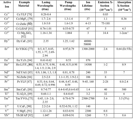
(29) Chapter 1 – Overview of DPSSLs Figure 9 - Array Pumping of Er:YSGG by SEL [after 77]. As the output and wavelength range available from laser diodes improves in the future, we can expect to see microchip lasers operating closer to their maximum quantum efficiencies with lower thresholds, providing real commercial competition for diode lasers and larger DPSSL systems. There will be a sustained increase in the number of ions and hosts that can operate in a microchip format, as new diode technology becomes available allowing access to new ions.. 1.3 Solid-State Laser Materials The aim of the second part of this chapter is to give a broad overview of solid state laser materials and the active ions involved. Active Ion. Example Material. Lasing Wavelengths (mm). Ce3+. Pump Wavelengths (mm). Ion Lifetime (ms). Emission XSection (10-20cm-2). Absorption X-Section (10-20cm-2). Ce:YLF [78]. 0.28-0.4. 2+. Co:MgF2 [79]. 1.7- 2.6. 1.3-1.4. 37. 1.1. Cr. 2+. Cr:ZnSe [80]. 1.8-3.0. 1.6-1.9. 4-13. 75-188. Cr. 3+. Cr:LiSAF [81]. 0.76-1.01. 0.55-0.75. 67. 5. 4.5. Cr. 4+. Cr:Mg2SiO4 [82]. 1.16-1.34. 1.064. 3. 14.4. 1-2cm-1. Dy2+. Dy:CaF2 [83]. 2.35. 1.25, 1.62. 4000050000. Er3+. Er:YSGG [77]. 0.5, 0.7, 0.85, 1.55, 1.77, 2.692.94. 0.97,0.79. 1300-2000. 2.6. 0.64 (Er:Yb). Eu3+. Co. 0.03 0.36. Eu:Y2O3 [84]. 0.61-0.62. 0.53. 870. 3+. Ho:LiYF4 [81]. 0.55, 0.75, 0.98, 1.4, 1.5; 2.36, 2.9. 0.48, 0.51,0.98. 14300. 1-2. 0.9. Nd3+. Nd:YAG [85]. 0.9, 1.06, 1.3, 1.8. 0.81, 0.78. 240. 33. 7. 2+. Ni:ZnSe [86]. 2.5-2.8. 1.1-1.35, 1.9-2.1. 106. 8. 3+. Pr:YLF [87]. 0.53, 0.6, 0.64, 0.69, 0.72; 0.996. 0.44, 0.47, 0.48, 0.59. 9-45, 160. 2-28. 0.8-2.4. Sm:CaF2 [88]. 0.7-0.77. 0.4-0.45,0.6-0.65. 1.4. 40. 300. Ti:Al2O3 [89]. 0.68-1.1. 0.4-0.65. 3.2. 32. 6. Tm:YVO4 [75]. 0.45, 1.8- 2.0, 2.35. 0.78-0.79. 2500-2700. 5.6. 3.5 (5%). U3+. U:CaF2 [90]. 2.2-2.6. 0.52-0.58, 1.12. 140. 2+. V:MgF2 [91]. 1.12-1.26. 0.83-0.91. 2300. 0.8. Yb:SFAP [92]. 1.047. 0.89-0.91. 1260. 7.3. Ho. Ni Pr. Sm2+ 3+. Ti. 3+. Tm. V. Yb. 3+. 8.6. Table 3 - Lasing Ion Properties 19.
(30) Chapter 1 – Overview of DPSSLs In particular we are interested in paramagnetic ions that show lasing through an electronic transition of a metal ion held in a solid matrix. In general to achieve stimulated emission the ion must possess a relatively long-lived (>1μs) excited state from which a radiative transfer occurs, to a short-lived (<100ns) terminating level.Table 3 details some of the active ions from which stimulated emission has been observed and some of the relevant parameters associated with the lasing transitions. The ions can be split into two broad groups: 1. The rare-earth ions, comprising the lanthanides (4F electrons) and actinides (5F electrons), have narrow transitions involving purely electronic F-F transitions. The outer, optically active electrons are shielded from the nucleus and the transition is not broadened by nucleon vibrational or rotational energy 2. The transition metal ions comprise members of the iron group (3D electrons) which have broad D-F transitions because of phonon assisted decay. The outer electron shell is not shielded from the nucleus and therefore is dependent on its energy state, through phonon interaction As can be seen from Table 3 lasing is possible over much of the visible and infrared spectrum, in both broadband tuning ranges and narrow lines, with varied pump absorption spectra. The lasing properties are quite different even for ions of the same element and vary as well according to the host matrix’s properties. We will now consider the two main classes of ion, and Nd3+ in particular, followed by a brief overview of the classification of hosts.. 1.3.1 Vibronic Laser Materials (Transition Metal Ions) The transition metals: Ce3+, Co2+, Cr3+, Ho3+, Ni2+, Sm2+, Ti3+ and V2+, are elements of the iron group of transition metals which exhibit broad band optical emission when excited. Johnson et al. [93] realised in 1963 that transitions of the 3D electrons of these ions are broadened through phonon interactions, making the transition energy dependent on the vibronic energy state of the nucleus of the active ion as well as its electronic state. This broadening can also be observed in the absorption bands making these ions ideal for pumping with broad-band sources, as sensitisers for other ions [94] and as passive Q-switch elements [95]. Figure 10 illustrates the energy levels of five of these ions. Normally each of the ions. 20.
(31) Chapter 1 – Overview of DPSSLs only has one suitable lasing transition. The broad absorption bands in the visible part of the spectrum for each ion can be seen at the top of the diagram, giving each its distinctive colour. The dotted line represents the upper limit of the phonon assisted terminating level for each ion, which normally is very close to the ground level. Therefore these ions are generally three-level systems, with the emission bandwidth decreasing and shifting to longer wavelengths as the gain crystal is heated. Therefore many of these gain crystals are operated well below room temperature in pulsed mode and pumped by flashlights because of the strong visible absorption. For example, flashlamp-pumped Ni:MgF2 has a threshold of ~100J and wavelength centre of 1.62μm at 22K, has a threshold of 1800J and centre wavelength 1.8μm at 240K [96].. Figure 10 – Transition schemes of phonon-terminated lasers. The dashed lines indicate the position of phonon levels [after 97] Non-radiative decay processes, which increase with temperature, limit the quantum efficiency of these ions further. For example, the broad upper-state energy levels are prone to excited state absorption because of their greater overlap with higher energy levels. This effect and others can greatly reduce the internal quantum efficiency of the lasing transition at higher temperatures [98]. The broadband emission is however very attractive and much effort has gone into developing suitable systems where these ions can be exploited while minimising the problems highlighted. Cr3+ and Ti3+ have been the most successful transition metal ions with Ti3+ reaching commercial importance through broadly tuneable Ti:sapphire lasers in the near-infrared. Cr3+ has come to prominence in more recent years through the development of high power AlGaInP diodes suitable for pumping Cr3+ around. 21.
(32) Chapter 1 – Overview of DPSSLs 670nm [99,100,101]. Cr4+ in the form of doped fosterite (Cr:Mg2SiO4) has helped spearhead this push for room temperature vibronic lasers because of its tuneability from 1130-1367nm when pumped by the 1064nm output of a Nd3+ laser and its good lasing performance [102]. The broad emission bandwidth and lower gain of these ions allows effective modelocking of these lasers with pulses down to several femtoseconds in an all-solid-state design [103,104,105], leading to many interesting and novel applications. More recently, diode-pumped vibronic microchip lasers have been demonstrated based on Cr:LiSAF [106]. Our own work in St.Andrews has shown these devices have very low thresholds with good output beam quality and emit over a wide wavelength range [107]. Their output power is generally limited by thermal considerations however, making them a niche market for miniature and pulsed laser systems. With refinement of host materials to provide better thermal management and development of new cavity geometries, vibronic laser materials are set to make a large impact on DPSSL and microchip laser research. Miniature lasers with wide tuning ranges in the infrared and visible spectrum have many potential applications and will be the basis of much new laser research in the next decade.. 1.3.2 Rare-Earth-Ion Doped Materials In contrast, rare-earth ions have narrow transition bandwidths, with limited broadening. Nd3+ is the most common rare-earth ion used, though recently there is a resurgence of interest in the other ions, in particular Yb3+, Er3+, Ho3+ and Tm3+.. 22.
(33) Chapter 1 – Overview of DPSSLs. Figure 11 – Operation schemes of crystal lasers that emit on purely electronic transitions [after 97] The electronic structure of some of the rare-earth ions is illustrated in Figure 11. Typically these ions have a number of photon decay routes from the upper state, providing different terminating conditions and the possibility of many different operating systems, some of which will be discussed later. The upper state lifetime is generally longer for these ions because of the narrower decay routes, though this also usually equates to the benefit of no excited state absorption. The effect of temperature also has much less of an impact and they can be operated under most conditions. The narrow absorption bands make flashlamp pumping inefficient, however they can be ideal for laser diodes of the correct wavelength, giving efficiencies in excess of 60% [108]. Before the availability of good quality, cheap, high power diodes a lot of work went into broadening the emission and absorption bands of these ions to make them more suitable for the wider band pumping of flash lamps. One approach was to use the splitting of sub-levels of the terminating level in a suitable host to broaden the emission bandwidth of the transition, though this was difficult in practice for some ions. Work has also gone into the development of disordered hosts, where the active ion occupies a number of different symmetry sites, which broadens the absorption and emission bands of the ion through the different dipole moments created by the different symmetries of the sites. Excitation-energy migration strongly connects the activator centres, giving efficient emission and absorption over a wide band [109]. 23.
(34) Chapter 1 – Overview of DPSSLs Laser Ion Nd3+. Transition F3/2 → I11/2. Sensitising Ions Cr3+, Ce3+. D4 → 7F5. Gd3+. H13/2 → 6H15/2. Er3+. I7 → 5I8. S2 → 5I8. Cr3+, Fe3+, Tm3+, Er3+ Yb3+. S3/2 → 4I13/2. Ho3+. I13/2 → 4I15/2. Yb3+. F9/2 → 4I15/2. Yb3+. F4 → 3H5. Cr3+. H4 → 3H6. Cr3+, Er3+. F5/2 → 2F7/2. Nd3+, Cr3+. T2 → 3A2. Mn2+. 4. 4. 3+. 5. Tb. Dy3+. 6. Ho3+. 5. 5. Er3+. 4 4. 4. Tm3+. 3 3. Yb3+ Ni2+. 2. 3. Table 4 Sensitised Laser Crystals [after 97] Co-doping with a sensitiser or donor ion is another alternative method of improving the efficiency of rare-earth doped laser hosts. Dexter [110] was the first to investigate this excitation-energy transfer and showed the most efficient transfer occurs when the emission spectrum is in resonance with the acceptor absorption spectrum. Many energy transfer schemes have been developed and some of the common ones are listed in Table 4. The multiple decay routes of the rare-earth ions have led to two distinctive effects being observed, which are not possible in the vibronic laser materials: 1. Cascade Systems: Nd3+, Dy2+, Eu3+, Pr3+, Tb3+, Tm3+, U3+, Yb3+ ions only have one metastable state. However Er3+ has five metastable states and Ho3+ has four, which can lead to cascade systems and multiple lasing transitions for a single pump transition. Cascade operation has been observed in Er3+, Pr3+, Er3+:Tm3+, Yb3+:Tm3+, Er3+:Ho3+ and Tm3+, allowing visible laser radiation through the upconversion of infrared pump radiation [97]. 2. Self-Saturating Transitions: this is where the terminating level has a longer lifetime than the metastable state and normally causes lasing to terminate. Codoped ions can however act as de-activators allowing transitions which normally will not lase to lase. An alternative method is to artificially remove the population in the lower level by exciting it into a new level. These methods have 24.
(35) Chapter 1 – Overview of DPSSLs allowed a number of transitions, particularly in Er3+ and Tm3+, to lase [97]. As can be seen the rare-earth ions have been explored in more detail than transition metal ions because their properties make laser design less stringent. Particular focus has been given to one of the rare-earth ions, the triply ionised neodymium ion, because of its attractive energy level structure and ease of doping. 1.3.2.1 Nd3+ Doped Materials Trivalent neodymium was the first rare-earth ion to be used in a gain material, and has remained the most commonly used active ion found in solid state lasers. The intense luminescence and absorption of the narrow energy levels of Nd3+ along with a workable fluorescence lifetime have helped Nd3+ achieve its dominance. The energy level structure of the Nd3+ ion is illustrated in Figure 12. It is traditionally pumped on either the 760nm or 810nm absorption bands though it can also be pumped in the green spectral region. The two main photon decay routes from the 4F3/2 metastable level are the 4F3/2 → 4I11/2 transition (producing radiation at ~1.06μm) and the 4F3/2 → 4I13/2 transition (producing radiation at ~1.3μm). Both of these are four level systems, giving efficient CW operation on these transitions at 300K and above, without significant population in the lower lasing level causing reabsorption. The third transition 4F3/2 → 4I9/2 (producing radiation at ~0.9μm) is a quasi-four level system, with the lower lasing level close to the ground level, having a significant thermal population. The fourth transition is two orders of magnitude weaker, though has been shown to lase at 1.83μm [111].. 12000. 4. S 913nm. 1064nm. 1342nm. 760nm. 8000. 810nm. 10000. -1. Energy [cm ]. 3 /2. 4. I. 6000. 1 5 /2. 4. I. 4000. 1 3 /2. 4. I. 2000. 1 1 /2. 4. 0. I. 9 /2. 25.
(36) Chapter 1 – Overview of DPSSLs Figure 12 – Energy Levels of Nd3+ Ion A wide range of pump sources have been used to excite the ion, from the more traditional laser diodes, Ti:sapphire laser and argon ion laser, to pyrotechnic sources, solar radiation and electron beams [109]. Table 5 details some of the commonly used crystalline Nd3+ hosts and their properties for lasing around 1064nm when pumped by an AlGaAs laser diode. Neodymium has been successfully doped into all the major types of hosts with respectably high concentrations and creditable lasing performance in all cases. Nd:YAG, as mentioned earlier, has good all round characteristics, although other hosts have particular properties which make them more suitable under specific circumstances. For example the broad and intense absorption band of Nd:YVO4 at 810nm makes diode pumping easier than for Nd:YAG, however its short fluorescence lifetime and large stimulated emission cross-section provide a poorer Q-switched performance. All of the materials in Table 5 have been shown to lase successfully in a microchip geometry. Further and more in-depth discussion of some of these materials will be given in the next chapter of this thesis, as we seek to compare their performance in a microchip environment. Nd3+ Doped Crystal (Doping Concentration) Oxides Nd:YAG (1.1%) Nd:YOS (1%) Nd:YVO4 (1%) Nd:GdVO4 (1%) Nd:MgO:LiNbO3 (0.2%) Nd:LMA (4%) Nd:LSB (10%) Fluorides Nd:SFAP (1%) Nd:SVAP (1%) Nd:YLF (1%). Stimulated Absorption @~810nm *10-19cm2. Stimulated Emission (@~1064nm) *10-19cm2. Fluorescence Lifetime μs. Reference. 0.7 0.99 2.7 5.1 0.2 cm-1. 3.3 0.9 12.2 7.6 1.8. 236 240 98 90 100. [112] [113] [114] [115] [116]. 6.1 cm-1 0.71. 0.4 1.3. 160 118. [117] [118]. 2.26 1.8 32.1cm-1. 5.4 5 1.87. 298 215 460. [119] [120] [121]. 26.
(37) Chapter 1 – Overview of DPSSLs Stoichiometric NYAB LNP. 5.6 cm-1 40 cm-1. 10.6 3.2. 60 120. [122] [123]. Table 5 Comparison of Common Nd3+ Doped Materials Nd3+ lasers will continue to dominate the market because of the mature technology associated with them and because they offer the best lasing performance of any of the rare-earth ions, if wavelength is not a critical factor. Much of the work reported in this thesis is on Nd3+ doped materials because of its attractive features and undoubtedly it will remain at the centre of microchip laser work.. 1.3.3 Classification of Host Matrices The matrix in which the active ions are placed can significantly alter the characteristics of the ion. The crystal field into which the ion is placed causes this change and can be crucial to the operating characteristics of the laser. For example, an isotropic crystal has a symmetric field, producing an unpolarised output. Conversely, for anisotropic crystals the asymmetry in the crystal field polarises the ion and emission. Each ion site in the matrix unit cell will experience a different field, and therefore different emission characteristics. This can be advantageous if you wish to produce a broadened output, but it will also increase non-radiative decay processes and decrease the intensity of the transition. Solid-state hosts can be divided into three main crystalline types, plus noncrystalline glasses, each with differing characteristics: 1. Oxides - oxides are typically grown by the Czochralski method giving high optical purity and big crystals with good yields [124]. Oxides have good thermal and mechanical properties, though one of their major problems is fluorescence quenching which limits the doping concentrations that can be achieved. 2. Fluorides - Fluorides are usually grown using the Bridgman technique, which can introduce stress into the crystals, but which can contain the often volatile substances used in the preparation of these crystals [124]. Fluorides suffer less from fluorescence quenching than oxides, though their. 27.
(38) Chapter 1 – Overview of DPSSLs thermal and mechanical properties are poorer. Interestingly these crystals usually have negative thermo-optical coefficients. 3. Stoichiometric Crystals – in self-activated, or stoichiometric, crystals the active ions are part of the crystal lattice giving much higher ion concentrations than for doping. For doped crystals with high doping concentrations, fluorescence quenching reduces the effective upper-state lifetime of laser ions [125], with the quenching dependent on the square of the concentration of doped ions. For stoichiometric crystals the quenching is linearly dependent on concentration, allowing concentrations up to two orders of magnitude higher [97]. These higher concentrations in turn lead to higher absorption coefficients and higher emission cross-sections and make these materials attractive as microchip gain materials. The first of this class of materials to be demonstrated was NdP5O14 (NPP) which was first end-pumped by a pulsed dye laser [126], but later work with diode lasers showed a lasing threshold of 7mW [127]. LEDs have also been used to end-pump both NPP and LNP [128]. NYAB is an interesting stoichiometric crystal with non-linear properties that allow for selffrequency-doubling and frequency tuning [129]. Approximately ten stoichiometric laser crystals have been demonstrated to date and this number is gradually increasing [97] 4. Glasses – although glasses are not crystalline, they are commonly used as the host material for rare-earth ions. In bulk form, the ease of fabrication of doped glasses makes them attractive for high power lasers, where largescale amplifiers are often required, although the lasing performance of the ion is generally weaker than for crystalline materials [130]. The other commonly used form of glass is fibre, again easily fabricated with the ability to dope it with many active ions. Fibre lasers can be attractive for a whole host of reasons because of the advantages of that particular geometry. Doping of rare-earth ions into crystalline hosts can take advantage of other host characteristics. Self-frequency doubled lasers [131,132], frequency modulated [133] and amplitude modulated lasers [134] have all been demonstrated using the host crystal’s properties. As an example, Er:Yb:LiNbO3 is an attractive material because of 28.
(39) Chapter 1 – Overview of DPSSLs its good non-linear properties and the high doping concentrations of Er3+ possible, and its increased sensitisation with Yb3+, makes diode pumping in a microchip format realisable [135,136]. Sequential two-photon absorption can also lead to the generation of green light from these devices using a 980nm diode pump [135]. With these advances in crystal technology, efficient laser diode pumping of many ions is now possible. Nd3+ and Yb3+ have been successfully pumped by AlGaAs diodes around 810nm and InGaAs diodes at 899nm respectively: Er3+ at 790, 980 and 1480nm, Pr3+ at 835nm, Tm3+ at 800nm and Ho3+ at 780nm. Presently there are more than 280 crystalline hosts in which stimulated emission from rare-earth ions has been observed and this number is increasing by at least two every year [109].. 1.4 The Future of DPSSLs DPSSLs form only a small part of world-wide laser sales, some $53 million out of a total of $2.8 billion per annum. Nevertheless, they represent one of the fastest growing laser markets, with a projected increase in sales of 49% for the coming year [137]. They are beginning to replace lamp-pumped solid state lasers in the lucrative markets of material processing and medicine and to compete with ion gas lasers in the instrumentation, sensing, measuring and optical storage marketplaces. Important in-roads have been made into a number of diode laser markets, such as telecommunications and optical storage, which account for more than 64% of all laser sales. The main barrier to faster sales and market dominance of DPSSLs is the price of laser diodes compared to flashlamps, though as demand increases this should change. Diode-pumped solid-state lasers offer a number of key advantages over laser diodes and these help to determine their marketability and applications: 1. Beam Quality - The output beam of a DPSSL typically is a close approximation to a circular, diffraction limited, TEM00, beam. In contrast laser diodes, especially higher power diodes, typically have a non-circular, high transverse mode output beam, dependent on the size of the emitting region. 2. Linewidth – The linewidth of a high power diode is typically several hundred 29.
Figure
![Figure 2 - Schematic of multiple quantum well laser array [after 16]](https://thumb-us.123doks.com/thumbv2/123dok_us/8600066.372384/15.595.121.544.529.731/figure-schematic-multiple-quantum-laser-array.webp)

![Table 4 Sensitised Laser Crystals [after 97]](https://thumb-us.123doks.com/thumbv2/123dok_us/8600066.372384/34.595.128.508.71.337/table-sensitised-laser-crystals-after.webp)
+7

Outline
Related documents
Results Neuroblastoma BE(2)-C cells showed increased expression of stem cell markers (nanog homeobox [NANOG] and octamer-binding transcription factor 4 [OCT4]), as well as
Table 4 Pairwise comparison of the mean difference values of serum angiotensin converting enzyme levels of the patients with ocular involvement of ankylosing spondylitis, behcet ’
The Master Fund is authorised in Luxembourg as a specialised investment fund and is managed by a management company, Ress Capital Fund Management SA, who acts
The geography of the second global shift is strongly determined by the educational and language abilities of the service workers located in low cost locations (Bryson,
• Ensure that all school staff routinely working with hazardous chemicals receives proper training in all phases of chemical management, including safe storage, proper use,
• In New York, only victims who are married or used to be married to their abuser or have a child with their abuser can apply for a civil domestic violence order of
The site is also open to potential impact to peat water levels and ground water from adjacent land management and other activities.. The land to the east is currently an open
Customer Information Management (CIM): The Key to Successful CRM in Financial Services.. Reputation – Managing the single greatest risk facing
