ODEF: an Interactive Tool for Optimized Design of
EMI Filters
M. C. Di Piazza, M. Luna, G. Vitale Istituto di Studi sui Sistemi Intelligenti
per l’Automazione (ISSIA)
Consiglio Nazionale delle Ricerche (CNR) Palermo, Italy
G. Ala, G. C. Giaconia, G. Giglia Dipartimento dell’Energia, Ingegneria dell’Informazione e Modelli Matematici
Università degli Studi di Palermo Palermo, Italy
P. Zanchetta
Department of Electrical and Electronic Engineering University of Nottingham
Nottingham, United Kingdom
Abstract— The impact of EMI filters on volume and weight of
power converters is significant. For this reason, filter’s size optimization is a strategic step towards the improvement of the power converter’s power density. An EMI filter design that follows a conventional procedure does not guarantee the selection of components/configuration leading to the best power density. Therefore, in order to help EMI engineers and scientists in pursuing a fast and effective choice of optimal discrete EMI filter components and configuration, a novel tool is proposed in this paper, namely ODEF (Optimized Design of EMI Filters). ODEF is an interactive software application running in Matlab® environment. It suitably improves a previously validated EMI filter design procedure that extends the conventional filter design method in order to achieve optimal power density. Features and operation of ODEF tool are illustrated. Moreover, the experimental assessment of an input EMI filter, designed according to the optimized procedure for an inverter-fed induction motor drive, is performed.
Keywords— EMI filter design, Power density, Power converters, Electrical Drives.
I. INTRODUCTION
Recently power electronics market has been boosted by new high-speed devices allowing faster switching operation as the wide-band gap devices based on Silicon Carbide (SiC) or Gallium Nitride (GaN) [1], [2]. On the other hand, their operation in power electronic converters leads to an increase of electromagnetic interference (EMI). For this reason noise filtering is, more than ever, one of the major issues in power electronic system design, particularly when dealing with stringent standard limits [3]-[5]. Besides satisfying EMI limits a further optimization in terms of filter size and weight can be performed. In fact, the EMI filter can contribute up to 30% of the total size and weight of power electronic converters; in some applications, such as airplanes, electric vehicles, etc., such an optimization is mandatory [6]-[8].
Scientific literature proposes several techniques dealing with high-power-density design of discrete EMI filters for
power electronic converters. Some techniques are based on setting up a compact layout by using suitable winding structures and/or high performance magnetic materials for the inductor cores [7]-[13]. Other approaches, starting from an accurate high frequency model of the system under investigation, propose the use of optimization algorithms to minimize either the volume of the whole EMI filter, i.e. related to common mode (CM) and differential mode (DM) sections, or the volume of some parts of it. It should be noted that a relevant computational effort is anyhow needed [10]. The use of heuristic procedures, mostly genetic algorithms, to perform an EMI filter design oriented to power density maximization, is proposed in [11]. A PC-based automatic EMI filter design method without any volume minimization implications is presented in [12]. Finally, a minimization of the DM EMI filter volume, utilizing some interpolated volumetric parameters, has been done in [13], where it is demonstrated that the selection of an optimal number of filter stages leads to the minimum occupied volume. However, this approach cannot be applied to minimize CM EMI filter volume.
In any case, regardless of the used method, the identification of the configuration leading to the best power density in terms of minimum volume/weight is a nontrivial task. Hence, it cannot effectively be managed manually by a time-consuming trial-and-error approach. A rule-based computer aided procedure for the optimized design of EMI filters in terms of power density has been proposed in [14]; it allows reducing the effort needed for properly selecting the components of both the CM and the DM EMI filter sections.
based on the optimized design procedure has been developed, namely ODEF (Optimized Design of EMI Filters).
ODEF is an interactive application running in Matlab® environment that enables a simple and fast selection of EMI filter components, circuit configuration and number of stages for achieving optimal power density. Furthermore, ODEF allows to compare the optimal EMI filter design to the suboptimal results, so as to leave the final choice to the designer. The effectiveness of the proposed design approach has been validated using a suitably devised experimental setup. In particular, the operation of ODEF tool has been illustrated and the assessment of an EMI filter designed according to the optimized procedure has been performed.
II. BASIC STEPS OF EMI FILTER DESIGN
The first step of the conventional EMI filter design is the identification of the crucial point on the experimental curve of the EMI emission, generally the emission peak at the lowest frequency within the EMI range (150kHz - 30MHz). Therefore, the CM and DM noise spectra have to be separately measured as the initial step of the design. The required attenuations Attreq_CM, Attreq_DM for the CM and DM noise are expressed as:
(1)
Attreq _ CM / DM =Ah _ CM / DM −L+SM
where Ah_CM, Ah_DM are the amplitudes of the harmonic to be
attenuated, L is the maximum amplitude allowed by the reference standard at the frequency of interest and SM denotes an additional safety margin usually set to 6 dBµV.
The cutoff frequency of the CM or DM filter is then expressed by (2), where fatt_h is the harmonic frequency to be
attenuated, Att_intr _filter is the filter inherent attenuation, which
is related to the filter circuit configuration, and n is the number of filter stages. When both corner frequencies are known, the inductance and capacitance values of the CM/DM sections of the EMI filter can be determined.
fatt _ h (2)
çn Att _ int r_ filter÷
ç ÷
10è ø
CM capacitance is fixed by standards to comply with safety issues (ground current), whereas DM parameters can be selected with some degrees of freedom, considering that the value of LDM will be reduced increasing the value of CDM , and
vice-versa. For this reason, the DM section design can consider either the case of a LDM obtained by the leakage inductance of
the CM choke (Lleakage=0.2÷2% LCM, depending on the core
material) or the case of a LDM realized by means of additional
inductors [14], [15].
In any case, geometrical dimensions and magnetic properties of the inductors’ cores must be appropriately selected so to prevent magnetic saturation, considering the maximum values of the CM/DM noise currents measured in time domain. Finally, the choice of the best number of filter stages comes from the best tradeoff between the required attenuation and the volume/weight of available commercial components.
æ Attreq ö
fo_CM / DM =
III. EMI FILTER OPTIMIZED DESIGN PROCEDURE
The optimized design procedure proposed in this paper starts from the basic principle illustrated in Section II, introducing the additional objective of pursuing the best power density for the EMI filter. It is based on a previously developed rule-based algorithm [14] that takes into account the main characteristics of the filter application: the power electronic circuits under study, the filter design constraints and a database with parameters extracted by datasheets of commercial components for the realization of EMI filters. This algorithm repeats the steps of the conventional design procedure for different configurations (e.g., varying core material and model, number of stages, etc.) and chooses the configuration exhibiting the best volume. In [14] it has been demonstrated that EMI filters designed according to the optimized procedure are more compact than those designed according to the conventional method. Furthermore, the filtering performance are comparable in both cases.
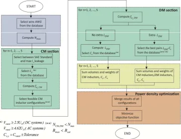
Here, such a design procedure has been suitably extended and improved. The obtained algorithm allows a more extensive evaluation of EMI filter components and configuration impact on power density in terms of both volume and weight; hence more effective results can be obtained. Furthermore, it does not discard suboptimal designs, allowing to compare them with the best solution. The overall concept and the different steps of the optimized procedure are summarized in Fig. 1, whose symbols are defined as follows. AWG: conductor diameter expressed in American Wire Gauge unit; n: number of filter stages in range 1÷5; Nmax : maximum number of turns for each core; Cy, Cx:
capacitance of phase-to-ground/phase-to-phase capacitors; Vrated , Crated : capacitors’ rated voltage/capacitance; UN: nominal
voltage of the power converter; Bmax , Bsat: maximum/saturation
magnetic induction. The proposed optimized design procedure has the following advantages with respect to the algorithm presented in [14]:
1. a new extended database is provided, including conducting wires and an increased number of commercial Cx and Cy
capacitors;
2. the volume/weight contribution given by the inductor wires (non-negligible when dealing with rated power of hundreds of volts and beyond) is included in the EMI filter calculations;
3. the filter design can be performed either on the basis of the measured CM/DM spectra (given as input and compared with the limits of a chosen standard) or explicitly giving the required CM/DM attenuations and frequencies;
4. the CM capacitance can be chosen either on the basis of SAE AES 1831 standard requirements or by explicitly setting the maximum ground leakage current;
5. the options of a LDM obtained by the leakage inductance of
the CM choke and of a LDM realized by an additional
inductor can be explored either alternatively or at the same time;
6. two coefficients can be provided by the user to optimize the design assuming any linear combination of volume and weight as the objective function;
Fig. 1. Flowchart of the proposed optimized EMI filter design procedure.
IV. ODEF APPLICATION
ODEF application is distributed as freeware for non- commercial use and it can be downloaded from www.issia.cnr.it/wp/?page_id=8070. The application has been designed using Matlab GUIDE to layout the user interface and by manually writing the code for the callback functions associated with each graphical object. It has a simple and intuitive user interface, which is organized in three tabs for increased usability, namely Noise Profile, Computation, Extra (Figs. 2-4). In particular, the main algorithm is executed interacting with the graphical objects of Computation tab, whereas the other tabs present additional features that complement the main algorithm. A general description of the implementation of ODEF and the main functionality of the application will be given hereinafter.
A. Starting the application and defining inputs
After installation, the application is simply started typing ODEF at Matlab® prompt. A window will open, as shown in Fig. 2. If the user already knows the required CM/DM attenuations and cutoff frequencies, he can directly switch to Computation tab and enter these values in the related fields of the third panel, together with filter topology (e.g., Γ, Π, T). The circuit schematic of the chosen filter topology will be shown in the upper right figure of the tab.
Then, the user can provide the other input quantities, filling the fields of the other panels. In particular, the system parameters to be entered in the first panel are the following: system type (frequency and number of phases), nominal
voltage, the maximum load current and maximum values of the CM/DM noise currents. In the second panel, the user can choose how to determine the value of the CM capacitors: either according to SAE AS 1831 standard (20 nF for 400 Hz systems; 100 nF in the other cases) or imposing a maximum leakage current. Furthermore, in the Extra_Ldm panel the user can express his preference about the realization of the DM filter. Choosing Always or Never the algorithm will include in the search space only the DM filters realized using an extra DM inductor or exploiting the leakage inductance of the CM choke, respectively. For example, aiming to achieve an increased reliability, the user might want to force the use of extra DM inductors to be sure that electrolytic capacitors are not used for the realization of the DM filter. On the other hand, if Auto is selected, the search space will include DM filters realized according to both techniques. Finally, the volume and weight coefficients of the objective function, expressed in percentage, can be entered in the last panel. If the user does not know the required CM/DM attenuations and frequencies, he can open Noise Profile tab and load previously acquired CM/DM noise spectra in Excel® file format or import them from Matlab® workspace. The data will be plotted in the two graphs of the tab. Then, selecting an item from the related drop-down menu, the user can choose a reference standard, whose limit curve will be superimposed on the data as a red line. The following reference standards are available: MIL- STD-461F, EN55011 class A, EN55011 class B, DO160F cat. B, DO160F cat. L.
[image:3.595.124.489.60.340.2]required attenuations, fills the related text boxes and highlights the related points on the graphs with red circles. At this point, the user can confirm the data and switch to the Computation tab to provide the other input data, as previously described.
B. Executing the algorithm
When the user clicks on the Compute button of the Computation tab the algorithm described in Section III is executed, processing the input values and the database content. Then, the results are shown in the Results panel of the same tab. In particular, the feasible filter configurations are arranged according to increasing values of the objective function and the Configuration drop-down menu is populated. When the user selects an item from this menu, the details about the chosen configuration, including the objective function’s value, are shown in the Results panel. Besides the numerical values of the physical quantities (e.g., LCM, Cx, Cy, etc.), other data are
extracted from the databases, e.g., wire type and code, core material and type, capacitor brand and model, etc. The obtained filter configurations depend on the specific components of the chosen database, which can easily be modified or expanded. In the latter case the execution time of the algorithm will increase, as expected. Finally, a series of buttons allow to load/save either the complete input dataset, including the CM/DM spectra, or the sorted set of feasible configurations. In this way, saved information can be recalled at later time.
C. Plotting data
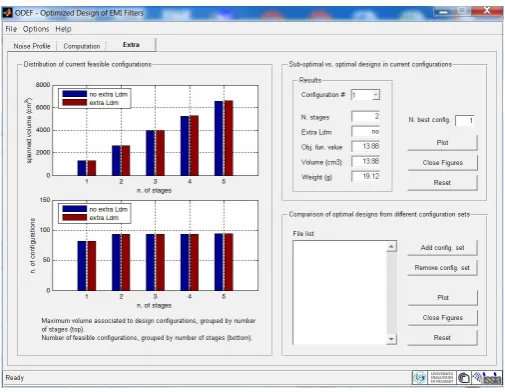
Sometimes, it is useful to compare suboptimal designs to the best solution returned by the algorithm. For example, it could happen that the best design is a two-stage filter, but the second best design is a one-stage filter, whose objective function’s value is slightly higher than the global minimum. In such cases, the designer could choose the second best design. For this purpose, besides exploring the Results panel of the Computation tab, it is possible to exploit the features of the Extra tab. In particular, after selecting the number of configurations to consider among the entire feasible set, it is possible to generate a series of comparative plots, as those shown in Figs. 6-10 of Section VI for the chosen case study.
Furthermore, it could be interesting to check whether the best design varies or not when the CM attenuation, imposed by the user, is higher than the minimum required value. Sometimes the best design remains the same, due to the discrete nature of the problem (discrete set of values for L and C, integer number of turns for the inductor windings, etc.). To this aim, a series of buttons of the Extra tab allow to load feasible configuration sets, previously saved after different runs of the algorithm, and to generate some plots that compare the best designs, as those shown in Figs. 11-12 of Section VI to discuss the results for the chosen case study.
V. EXPERIMENTAL RIG
A suitable experimental rig has been arranged to validate the proposed computer-aided procedure. It is composed of a PWM IGBT Voltage Source Inverter (VSI) that supplies a three-phase induction motor with the following characteristics:
Fig. 2. Screenshot of ODEF application: Noise Profile tab.
Fig. 3. Screenshot of ODEF application: Computation tab.
[image:4.595.307.558.53.244.2] [image:4.595.306.559.270.465.2] [image:4.595.306.559.490.686.2]rated voltage UN = 48 V, rated power PN = 220 W, maximum
current Imax = 5 A. The VSI is based on a STGIPS10K60A
power module and on an Altera Cyclone III FPGA board implementing the PWM modulator. The VSI switching frequency is equal to 20 kHz, whereas the output voltage is 48 V. A dual DC Line Impedance Stabilization Network (LISN) with a voltage capability up to 600 V has been set-up and used to measure the conducted EMI [16]. The experimental rig has been equipped with a R&S FSH4 (100kHz-3.6GHz) spectrum analyzer and a RF current probe R&S EZ-17 for measurements in the frequency range 20Hz-100MHz with a maximum DC current of 300 A.
Fig. 5 shows a scheme of the experimental arrangement of the system under study. It should be noted that PWM inverter- fed loads/induction motor drives supplied by a DC power line, such as the considered one, are very common; for example they are frequently used either in vehicle applications (road vehicles, marine vehicles, aircrafts) or in DC distribution systems, such as those used in some residential/commercial smart buildings for energy saving [17]-[18].
Fig. 5. Scheme of the experimental rig.
VI. EXPERIMENTAL VALIDATION AND DISCUSSION
The measured CM/DM spectra, shown in Fig. 2, have been loaded into ODEF application and the automatic processing returned the following filter parameters:
• Attreq_CM = 30 dBμV@150 kHz; • Attreq_DM = 60 dBμV@170 kHz.
Then, the input data shown in Table I have been entered and the computation has been started. The application selected the best design (2 stages, no extra LDM , CM core index 27, total
volume=13.88 cm3) among a total of 910 feasible
[image:5.595.316.549.63.273.2] [image:5.595.41.286.297.398.2]configurations. All the details of the optimized EMI filter are given in Table II.
TABLE I. INPUT DATA FOR ODEF APPLICATION.
Filter topology Γ-Π
Reference standard Military Standard 461F
System type DC system
UN 48 V
Imax 5 A
Icm_max 32 mA
Idm_max 150 mA
Cy standard SAE AS 1831
Volume coefficient 100%
Weight coefficient 0%
Extra_Ldm_mode Auto
TABLE II. FEATURES OF THE OPTIMIZED EMI FILTER.
Number of stages 2
LCM @10kHz 126 µH (each stage)
Maximum magnetic
induction 0.237 T (each stage)
CM inductor core dimensions
(mm x mm x mm) 12x8.0x4.5 (each stage)
CM core AL@10kHz
28 µH
(Vitroperm 500F, model T60006- L2012-W902) (each stage) Number of turns per CM
winding 3 (each stage)
C CM 100 nF (each stage)
Cy 47 nF, ceramic, 250V, (Murata RDER72E473K2) (each stage)
LDM @10kHz 252 nH (L leakage =0.2% LCM ) (each
stage)
CDM 33 µF, electrolytic, 160 V, (Kemet
ESG336M160AH4) (each stage)
Wire size 15 AWG
Volume 13.88 cm3 (all stages)
Weight 19.12 g (all stages)
Finally, the features of the Extra tab have been used to analyze and compare the feasible configurations, which can be classified as shown in Fig. 6, according to the number of filter stages and to the presence/absence of the extra DM inductor. As the figure shows, the search space is quite large and the filter volume reaches 6591 cm3 in the worst configuration. In
order to provide an insight into the configurations that belong to a small neighborhood around the optimal solution, Figs. 7-8 show the distribution of the 15 best designs.
no extra Ldm extra Ldm
1 2 3 4 5
8000 6000 4000 2000 0 3 s pa n n ed v ol u m e ( cm ) n. of co nf ig u ra ti ons
n. of stages
no extra Ldm extra Ldm
1 2 3 4 5
0 150
100
50
n. of stages
Fig. 6. Distribution of all feasible configurations.
no extra Ldm extra Ldm
1 2 3 4 5
50 40 30 20 10 0 3 n. o f con fi g ur a ti o ns s p anne d v o lum e (c m )
n. of stages
no extra Ldm extra Ldm
1 2 3 4 5
5
0 15
10
n. of stages
[image:5.595.353.518.393.524.2] [image:5.595.355.518.565.692.2] [image:5.595.51.276.596.718.2]1-stage 2-stage 3-stage 0 20 40 60 80 100 120
core index 22
21
20
19
18
17
16
15
14
13
3
vo
lu
m
e
(cm
)
Fig. 8. Scatter plot of the best 15 configurations.
1 2 3 4 5
n. of stages 5
0 35
30
25
20
15
10
3
vo
lu
m
e
(cm
)
Fig. 9. Volume of the best configuration for each number of stages.
1-stage 2-stage 3-stage 4-stage 5-stage
0 10 20 30 40 50
configuration n. 40
35
30
25
20
15
10
3
vo
lu
m
e
(cm
[image:6.595.89.250.61.194.2])
Fig. 10. Distribution of the best 100 configurations for different n. of stages.
Furthermore, to evaluate the proximity of the returned solution to other configurations, Fig. 9 shows the volume of the best configuration for each number of stages and Fig. 10 presents the distribution of the best 100 configurations grouped for number of stages (50 for n=1, 29 for n=2, 11 for n=3, 8 for n=4, 2 for n=5). With reference to Fig. 10, the intersection of the curves related to 1-stage and 2-stage configurations demonstrates that the optimized design for achieving the best power density is a non-trivial problem. Therefore, it cannot effectively be managed by a trial-and-error approach.
As a further analysis, the design procedure has been repeated several times for increasing values of the desired CM attenuation, starting from the minimum required value and
keeping the other input parameters constant. The following range has been swept: [30, 32, 34, 36, 38, 40, 42, 44, 46, 48, 50, 52, 54, 56] dBμV.
Figs. 11-12 show the obtained results in terms of volume, number of stages and CM core index. In the considered case, the best configuration for each value of CM attenuation does not require the use of an extra DM inductor.
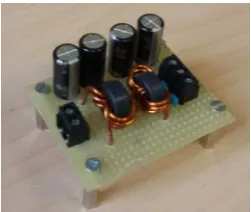
[image:6.595.87.248.232.365.2]It is worth noting that, as Fig. 11 shows, the CM attenuation of the filter can be increased up to 40 dBμV without increasing the design volume. This corresponds to an extra 10 dBμV safety margin that allows obtaining a better filter performance, balancing further possible non-idealities in the filter realization. The optimized EMI filter, designed according to the data of Table II and shown in Fig. 13, has been experimentally realized. Then, an experimental test has been performed to assess the filter performance within the inverter-fed induction motor drive described in Section V.
As shown in Fig. 14, the optimized designed filter exhibited a satisfactory behavior since the filtered EMI was below the standard limit (Military Standard 461F [19]). Therefore, without significant computational effort, the proposed EMI filter design method allowed obtaining the compliance of the power electronic system under study with the chosen standard using an EMI filter with optimized compactness and power density.
30 35 40 45 50 55 60
CM attenuation (dBμV) 18.5
18
17.5
17
16.5
16
15.5
15
14.5
14
13.5
3
vo
lu
m
e
(cm
[image:6.595.353.518.365.496.2])
Fig. 11. Volume variation of the best design for increasing CM attenuation.
30 35 40 45 50 55 60
1 2
n. of
st
age
s
30 35 40 45 50 55 60
CM attenuation (dBμV)
1 10 20 30 40
C
M
c
o
re
in
dex
[image:6.595.86.249.404.532.2] [image:6.595.360.529.545.676.2]Fig. 13. Photo of the optimized EMI filter.
Fig. 14. Measured EMI emission with/without the optimized EMI filter.
CONCLUSIONS
This paper proposes an interactive software tool for the optimized design of discrete EMI filters in terms of power density, namely ODEF (Optimized Design of EMI Filters). ODEF is an application running in Matlab® that allows a simple and fast selection of EMI filter components, circuit configuration and number of stages leading to the minimum overall filter volume/weight. Furthermore, ODEF allows to compare the optimal EMI filter design to the suboptimal results, so as to leave the final choice to the designer.
The effectiveness of the proposed design approach has been validated using a suitably devised experimental setup, based on an inverter-fed induction motor drive. Specifically, the operation of ODEF tool has been shown and the performance of an EMI filter, designed according to the proposed optimized procedure, has been assessed experimentally.
ACKNOWLEDGMENT
This paper has been funded by the following research projects: 1.CNR per il Mezzogiorno; 2. RITmare; 3. TESEO.
REFERENCES
[1] J. Millán, P. Godignon, X. Perpiñà, A. Pérez-Tomás, J. Rebollo, “A survey of Wide Bandgap Semiconductor Devices”, IEEE transactions on Power Electronics, vol. 29, pp. 2155 - 2163, May 2014.
[2] P. Gammon, “Silicon and the Wide Bandgap Semiconductors, shaping the Future Power Electronics Device Market”, 14th International
Conference on Ultimate Integration on Silicon (ULIS), 19-21 March 2013.
[3] G. L. Skibinski, R. J. Kerkman, D. W. Schlegel, “EMI Emissions of Modern PWM AC Drives”, IEEE Ind. Electron. Magaz., pp.47-81, Nov./Dec.1999.
[4] M. Silva, N. Hensgens, J. Oliver, P.Alou, “New considerations in the input filter design of a three-phase buck-type PWM rectifier for aircraft applications”, IEEE Energy Conv. Congr. Exp., pp. 4087 – 4092, 2011. [5] M.C. Di Piazza, A Ragusa, G Vitale, “Power-loss evaluation in CM
active EMI filters for bearing current suppression”, IEEE Trans. Ind. Electron., vol. 58, pp. 5142-5153, 2011.
[6] J. W. Kolar, U. Drofenik, J. Biela, M. L. Heldwein, H. Ertl, T. Friedli and S. D. Round, “PWM Converter Power Density Barriers”, Power Conversion Conference (PCC ’07), Nagoya, 2007.
[7] G. Ala, M. C. Di Piazza, G. C. Giaconia, G. Giglia, G. Vitale, “Design and performance evaluation of a high power density EMI filter for PWM inverter-fed induction motor drives”, IEEE 15th International Conf. on Environment and Electrical Engineering (EEEIC 2015), 10-13 June 2015, Rome, Italy, pp. 1573-1579, DOI: 10.1109/EEEIC.2015.7165406. [8] G. Ala, M. C. Di Piazza, G. C. Giaconia, G. Giglia, G. Vitale, “Design
and performance evaluation of a high power density EMI filter for PWM inverter-fed induction motor drives”, IEEE Trans. Industry Applicatons,
vol. 52, no. 3, pp. 2397-2404, May-June 2016, DOI:
10.1109/TIA.2016.2518129.
[9] Y. Maillet, Rixin Lai, Shuo Wang, Fei Wang, R. Burgos, D. Boroyevich, “High-Density EMI Filter Design for DC-Fed Motor Drives”, IEEE Trans. Power Electron., vol. 25, pp. 1163-1172, May 2010.
[10] B. Toure, J.L. Schanen, L. Gerbaud, T. Meynard, J. Roudet, R. Ruelland “Optimal EMC Modeling of Drives for Aircraft Applications: Modeling Process, EMI Filter Optimization, and Technological Choice”, IEEE Trans. Power Electron., vol. 28, pp. 1145-1156, March 2013.
[11] F. Wang, W. Shen, D. Boroyevich, S. Ragon, V. Stefanovic, M. Arpilliere, “Design Optimization of Industrial Motor Drive Power Stage Using Genetic Algorithms”, Power Electronics and Motion Control Conference (IPEMC 2006), 2006.
[12] Huang-Jen Chiu, Tian-Fu Pan, Chun-Jen Yao, and Yu-Kang Lo, “Automatic EMI Measurement and Filter Design System for Telecom Power Supplies”, IEEE Trans. Instrum. Meas., vol. 56, pp. 2254-2261, Dec. 2007.
[13] K. Raggl, T. Nussbaumer, J.W. Kolar, “Guideline for a Simplified Differential-Mode EMI Filter Design”, IEEE Trans. Ind. Electron., vol. 57, pp. 1031-1040, March 2010.
[14] G. Ala, G. C. Giaconia, G. Giglia, M. C. Di Piazza, M. Luna, G. Vitale, P. Zanchetta, “Computer Aided Optimal Design of High Power Density EMI Filters”, accepted for presentation at IEEE 16th International Conf. on Environment and Electrical Engineering (EEEIC 2016), 7-10 June 2016, Florence, Italy.
[15] Yoann Y. Maillet, “High-Density Discrete Passive EMI Filter Design for Dc-Fed Motor Drives”, Master Thesis, Dept. of Elect. Eng., Virginia Polytechnic Institute and State University, Blacksburg, VA, 2008. [16] M. C. Di Piazza, A. Ragusa, G. Vitale, “Common Mode EMI
Propagation in High Voltage DC supplied Induction Motor Drives for Electric Vehicles Application”, IEEE International Electric Machines and Drives Conference (IEMDC 2009), pp. 647–652, 3-6 May 2009. [17] S. Anand, B. G. Fernandez, “Optimal voltage level for DC microgrids”,
in Proc. 36th Annual Conference on IEEE Industrial Electronics Society (IECON 2010), pp. 3034-3039, 2010.
[18] H. Kakigano, N. Nomura, T. Ise, “Loss evaluation of DC distribution for residential houses compared with AC system”, in Proc. 2010 International Power Electronics Conference (IPEC), pp 480-486, 2010. [19] “Requirements for the control of electromagnetic interference
characteristics of subsystems and equipment”, Military Standard 461F, Dec. 2007.
[image:7.595.47.279.190.331.2]