Reliable Integration of a high performance multi-chip half-bridge SiC power module
Bassem Mouawad, Jianfeng Li, Alberto Castellazzi, C. Mark Johnson Power Electronics, Machine and Control Group (PEMC)
University of Nottingham
University Park Campus, NG7 2RD, Nottingham, United Kingdom Email: [email protected]
Abstract
Silicon carbide (SiC) devices have been adopted to push the boundaries further in terms of power density, conversion efficiency, switching speed or thermal capability. To have the benefit of such semiconductors, new packaging should be developed to meet all the advantages. In this paper, we present a reliable integrated concept of a new packaging solution for multi-chip SiC devices aiming to have a very low parasitic inductance in order to have high switching frequencies and ensure a good reliability for long-term operation.
Introduction
Silicon carbide (SiC) devices have been adopted to push the boundaries further in terms of power density, conversion efficiency, switching speed or thermal capability. In fact, they are enabling components mainly if higher switching frequencies in power electronics are considered. However, this trend imposes new challenges towards the package of these devices where stray parasitic inductances become crucial concern [1]. Hence, new packaging solution is needed to reduce the stray parasitic inductance for addressing this concern and some packaging solutions have been reported [2]–[4]. On the other hand, the reliability is key role in order to ensure a long-term operation of such a package.
The work presented here consists of a new packaging concept, which enables new possibilities of power track routing and leading to a significant reduction in commutation inductance. This requires the use of a
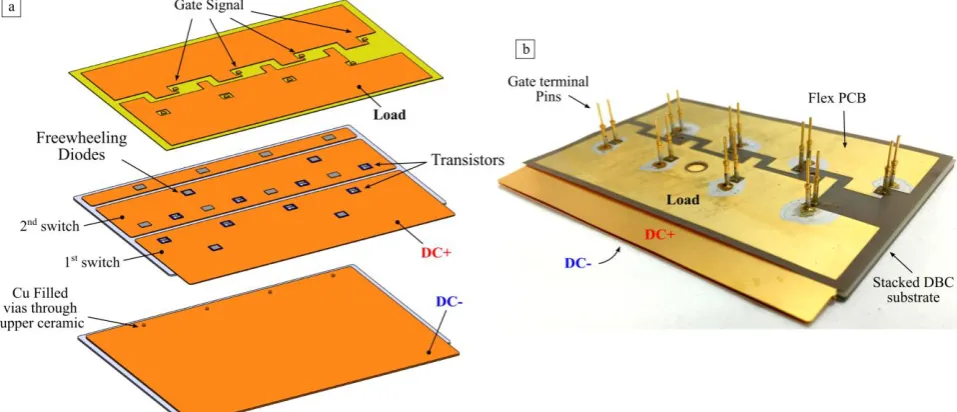
stacked DBC substrate (Cu/ceramic/Cu/ceramic/Cu) that allows the power lines to be overlapped and forming a parallel plate structure (Figure 1). This geometry is to cancel the magnetic field as much as possible and hence minimizing the stray parasitic inductance generated when the current flows through these plates. The connection between the top and middle Cu layer is achieved by Cu filled vias through the upper ceramic layer. A flex PCB is mainly used to replace the bond wires. It consists of two conductive layers. The lower layer connects the devices to the top conductive layer of the flex PCB. From the electrical point of view, the thinner the ceramic is, the lower the inductance. However, the thermal and mechanical behaviour of such packaging concept must be investigated.
This design was recently reported [5][6]. This paper is concerned with the thermomechanical reliability of a stacked substrate–chip–flex PCB assembly that has been constructed with soldering technology for implementation of an integrated power module. The assembling process followed to build the package shown in Figure 1b is listed. Then, the 3D finite-element (FE) modelling had been employed to simulate the thermomechanical response of the designed assembly under the reflow processes and an accelerated thermal cycling test between −55 and +150 °C.
Parts and assembly process of the designed package The designed package contains the following:
Stacked DBC substrates; this consists of 0.3mm Cu/ 0.635mm AlN/0.6mm Cu/0.635mm AlN/0.3mm Cu
[image:1.595.73.552.529.735.2]Flexible PCB; this consists of 0.1mm Cu / 0.1mm polyimide / 0.1mm Cu
SiC JFETs normally on devices with Cu metallisation on top
External anti-parallel SiC diodes
Ag pins for connecting the flex PCB to the stacked DBC substrates
Cu pins as gate terminal
The stacked DBC substrates were custom ordered and bonded by the supplier using a conventional reflow process with SnAgCu solder alloy.
Prior to the assembling process, both the Flex PCB and Cu-based SiC JFETs and SiC Diodes are chemically cleaned using acetone and isopropanol solutions. Plasma etching was then used to remove any residual organic contamination and for deoxidization of SiC devices.
First, Sn-3.5Ag solder paste was stencil-printed on the copper track of the Flex PCB. Because the SiC JFETs have relatively fine patterns, an accurate die bonder had been employed for accurate die placing to avoid potential short-circuiting between the gate and source. The Flex PCB with the SiC devices was then heated to melt the solder paste and to form the connection between the Cu tracks of the Flex PCB to the Cu track on the topside of the SiC devices.
Thermomechanical Modelling
In order to have an insight on the behaviour of the such package under different heat treatment; i.e. solder reflows processes and thermal cycling, a thermomechanical simulation was then used to investigate the weakpoints and the possible high stress and/or high creep strain area that could lead to a major failure of the
package.
We assumed that the physical structure and the SiC JFETs distribution is symmetric, so the thermomechanical model is then simplified to cover only 2x SiC JFET on each switch. Figure 2 shows a view of the representative meshing systems to discretize the half of the design and cross-sectional view with a close-up view showing all the parts and the meshed layers. Furthermore, the SiC diodes were not included in the simulation, as the final version of the package won’t contain external anti-parallel diodes.
The materials used for this simulation are as follow: DBC substrates each has 0.3mm Cu/ 0.635mm AlN/0.3mm Cu
0.1mm SnAgCu solder alloy to bond the two DBCs together
Backside joint: 0.1mm Sn37Pb solder; SiC JFETs: 0.11mm
Topside joint: 0.1mm Sn-3.5Ag solder Ag pins: 0.11mm thick silver
Flex PCB: 0.1mm Cu/0.1mm polyimide/0.1mm Cu 0.1mm Sn37Pb solder to bond the Gate terminal pins on the flex
It should be pointed out that the formation of intermetallic compounds (IMC) at the solder/contact metallisation interfaces have been neglected, because the IMCs are extremely thin when compared to other materials and parts in the model, and would require extremely fine elements to discretize them. Therefore, the formation and growth of the IMCs in this model have been ignored.
On the other hand, it should be pointed out that the shapes of the solder joints shown in Figure 2 are ideal
Figure 2 (a) Cut view of the representative meshing systems to discretize the half of the design and (b) cross-sectional view with a close-up view showing all the parts and the meshed layers
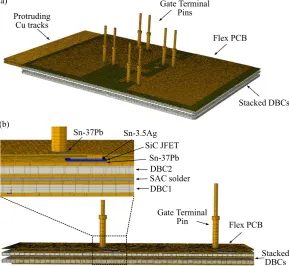
Protruding Cu tracks
Gate Terminal Pins
Flex PCB
Stacked DBCs (a)
DBC2
DBC1 SAC solder Sn-37Pb Sn-37Pb
Gate Terminal Pin Sn-3.5Ag
SiC JFET
Flex PCB
[image:2.595.167.457.466.732.2]approximations for subsequent FE modelling and simulation, and those of the actually reflowed solder joints might vary somewhat.
Moreover, in the final version of this prototype, the package will be filled with a soft dielectric encapsulant. This has been ignored because silicone gel, which is commonly used as the encapsulating gel, has extremely low thermal conductivity and Young’s modulus compared to the other components and parts in the assembly.
The thermal and mechanical properties of all the materials used for the simulation were taken from [7]–[9]. In particular, Chaboche’s plastic model was used to describe the mechanical properties of the Cu, and Anand’s creep model was used to describe the mechanical properties of all the solder alloys. For all the rest of materials, only linear elastic properties have been considered.
Meshing System
The thermomechanical modelling and simulation has been done using commercial available FE analysis software Abaqus 6.14 and its graphic user interface CAE. The meshing system used to discretize the half assembly model was determined through a few trials to ensure that the simulation can be executed with a desktop PC. It mainly consists of 350453 C3D8R linear brick or C3D6 linear triangular prism elements, plus minor C3D10 quadratic tetrahedron elements. The elements with varied sizes have been used. If all the triangle prism and tetrahedron elements are changed to the corresponding brick elements for comparison, the largest element is approximately 1 1 0.476mm, and the smallest element is 0.556 0.365 0.025mm. Relatively small and thin elements have been used to discretize the solder joints in which the stress and strain developments are mainly
concerned in the present work. Thermal history
The assembly was first subjected to a predefined temperature profile to simulate the stress and strain developments during the two-step reflow soldering process. During both soldering steps, the corresponding solder joints were deactivated without the development of stress and strain when they were in the form of either solder paste or molten solder. They were activated when they solidified from the molten solder. Both the solder paste and the solid solder joints are molten at the melting point of 221°C, and the solidification of the molten solder occurs at a supercooling temperature of 192°C for Sn-3.5Ag solder alloys.
[image:3.595.318.549.74.246.2]Then, the thermomechanical response of the assembly
Figure 3 Thermal history of predefined temperature profile of the two soldering steps followed by one thermal
cycle between −55 and 150 °C.
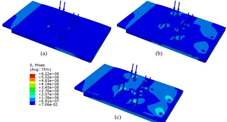
Figure 4 Distribution of the von Mises stress with unit in Pa of the simulated structure after (a) the SAC reflow step, (b) the reflow of Sn37Pb and (c) one thermal cycle between –55 to 150°C
(a)
(b)
[image:3.595.75.545.485.737.2]associated with one cycle of thermal cycling between −55 and +150°C, as shown in Figure 3, were simulated. The same approach was applied on an integrated package using 5 thermal cycles [10]. For the thermal cycling, a predefined uniform temperature field in the entire assembly was directly applied to simulate further stress and strain developments.
For the aforementioned thermomechanical simulation, all the parts in the assembly have been assumed to have a zero stress and strain state at the beginning of the first soldering step.
Simulation results
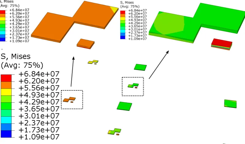
[image:4.595.140.357.75.298.2]From the simulation results, it was observed that the stress and strain developments in all the solder joints are independent of the initial stress and strain state in the DBC substrates. Figure 4 shows the distribution of the von Mises after each of the three steps shown in Figure 3. It’s shown the stress accumulation at the solder level between the device and the flex PCB. Figure 5 shows the distributions of the creep strain accumulation in the topside solder joints after the second reflow process, where Figure 6 shows the distributions of the von Mises
Figure 5 Distribution of the creep strain accumulation in the topside solder layer between the SiC JFET and the Cu tracks on the flex PCB, after the first SAC assembly
[image:4.595.112.512.485.720.2]stress at the latter.
The locations of the maximum residual stresses and the maximum creep/plastic strain accumulations in the solder joints may be different. For example, in the as-assembled module, the maximum Mises stress in the SAC solder joints occurs within one joint to connect the gate of one JFET to the flexible PCB and at the interface between the solder and the flexible PCB, while the maximum creep strain accumulation occurs within another joint to connect the source of one JFET to the flexible PCB and at the interface between the solder and JFET. This should be understood because the further creep strain development may lead to the release of the residual thermal stress to some extent and the failure of the solder joints is more related to the creep strain accumulation.
These results are readily understood because the stress and strain developments in the different materials are controlled by the mismatches of coefficients of thermal expansion (CTEs) between the materials and the accu- mulations of plastic and/or creep strains in the Cu, the flex and the solder alloy. Hence, using controlling or matching the CTEs (for eg. ceramic materials instead of polyimide) is essential in the current structure, first to ensure a good insulation and second to provide a better mechanical support for the package.
Single JFETs characterisation
Single SiC JFETs were then assembled using the same bond materials listed before, but with small peace of flex PCB, and one DBC substrate. Figure 7 shows the vehicle of test used for power cycling of a single SiC JFETs. Underfilling materials were used to provide a good mechanical structure. Unfortunately, either the solder of the gate pad or the solder of the source pad between the JFET and the Flex PCB were the weakest point in the samples with or without the underfilling materials (cf. Figure 8). This can be linked to the result obtained from the thermal simulation were the majority of the stress and or creep accumulations are located at this level of the assembly.
Conclusions
A novel packaging solution for integrated multi-chip SiC power devices is presented. The designed package offers the possibility to obtain a very low parasitic inductance and hence be beneficial for such semiconductor materials.
The assembly process is then listed. A FE thermomechanical modelling is then used to investigate all the thermomechanical performance induced after the soldering reflow process and the thermal cycling. The weakest point was found to be at the solder layer between the topside of the JFET and the Flex PCB with a high stress/strain accumulation. That point should be considered in the future and investigate an alternative material to replace the polyimide, for instance, with ceramic to provide a better mechanical support to the package.
Acknowledgments
This work is supported by the SPEED (Silicon Carbide Power Technology for Energy Efficient Devices) Project funded by the European commission FP7-Grant #:604057.
References
[1] R. Bayerer, “Parasitic inductance hindering utilization of power devices,” in 9th International Conference on Integrated Power Electronics Systems (CIPS), 2016. [2] R. Bayerer and D. Domes, “Power circuit design for
[image:5.595.104.528.76.235.2]clean switching,” in 6th International Conference on Figure 8 Photo showing the failed sample without
underfilling material. The flex PCB was intentionally bended for the photo.
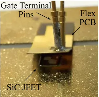
Gate Terminal
Pins
Flex
PCB
SiC JFET
Figure 7 Single DBC vehicle test for power cycling test showing in (a) the Gate terminal pins, SiC JFET bonded between the flex PCB and the DBC and in (b) the same with underfilling materials
Gate Terminal
Pins
Flex PCB
(a)
(b)
Underfilling
[image:5.595.108.269.569.727.2]Integrated Power Electronics Systems (CIPS), 2010, pp. 1–6.
[3] E. Hoene, A. Ostmann, and C. Marczok, “Packaging
Very Fast Switching Semiconductors,” in 8th
International Conference on Integrated Power Electronics Systems (CIPS), 2014, pp. 502–508. [4] P. Beckedahl, M. Spang, and O. Tamm,
“Breakthrough into the third dimension – Sintered multi layer flex for ultra low inductance power
modules,” in 8th International Conference on
Integrated Power Electronics Systems (CIPS), 2014, pp. 461–465.
[5] B. Mouawad, J. Li, A. Castellazzi, C. M. Johnson, T. Erlbacher, and P. Friedrichs, “Low inductance 2.5kV
packaging technology for SiC switches,” in 9th
International Conference on Integrated Power Electronics Systems (CIPS), 2016.
[6] B. Mouawad, J. Li, A. Castellazzi, and C. M. Johnson, “Low parasitic inductance multi-chip SiC devices
packaging technology,” in 18th European Conference
on Power Electronics and Applications (EPE’16 -ECCE), 2016.
[7] A. Zéanh, O. Dalverny, M. Karama, E. Woirgard, S. Azzopardi, A. Bouzourene, J. Casutt, and M.
Mermet-Guyennet, “Thermomechanical modelling and
reliability study of an IGBT module for an aeronautical application,” in International Conference on Thermal, Mechanical and Multi-Physics Simulation and Experiments in Microelectronics and Micro-Systems (EuroSimE 2008), 2008, pp. 1–7. [8] A. Zéanh, O. Dalverny, M. Karama, and A.
Bouzourene, “Lifetime and reliability assessment of AlN substrates used in harsh aeronautic environ- ments power switch modules,” Adv. Mater. Res., vol. 112, pp. 113–127, 2010.
[9] W. W. Sheng and R. P. Colino, Power electronic modules, design and manufacture. CRC press, 2005. [10] J. Li, A. Castellazzi, T. Dai, M. Corfield, A. K.