Research Paper
Need for Variable Frequency Control in DC-DC Switching Converters–
Challenges and Opportunities using Digital Implementation
K HARIHARAN and SANTANU KAPAT*
IIT-Kharagpur, Kharagpur, West Bengal 721 302, India
(Received on 04 April 2017; Revised on 12 November 2017; Accepted on 13 November 2017)
DC-DC converters play a vital role in efficient power management in various portable devices. However, the challenges remain in achieving fast dynamic performance, stable periodic behavior, and high efficiency over a wide operating range. In the context of fixed-frequency pulse-width modulation (PWM), a multi-loop current-mode control (CMC) scheme offers improved bandwidth and superior line regulation compared to a single-loop voltage-mode control (VMC) scheme. However, CMC suffers from sub-harmonic oscillations while operating with the steady-state duty ratio D > 0.5, which requires a compensating ramp for stabilization. A compensating ramp eventually degrades the closed-loop bandwidth, and a further increase in the ramp slope would tend to approach VMC; thus the benefits of CMC are lost with an increasing duty-ratio. On the other hand, variable-frequency CMC methods, such as hysteresis control and constant on/off-time control techniques do not suffer from inner current-loop stability problems, and also offer improved transient response and light-load efficiency. However, undesirable steady-state frequency variations complicate the input filter design and may eventually lead to EMI problems. While a digital platform is helpful for fast and precise frequency regulation using an all-digital-PLL, the choice of sampling frequency remains an important concern for implementing variable-frequency digital control. This paper highlights the challenges and scopes using variable-frequency digital control. The paper also presents event-driven digital control solutions and design insights for next-generation power management solutions.
Keywords: Variable-Frequency Digital Control; Event-Driven Sampling; DC-DC Converters; Constant On-Time Modulation; Constant Off-On-Time Modulation
*Author for Correspondence: E-mail: [email protected]
Proc Indian Natn Sci Acad 84 No. 3 September 2018 pp. 657-668
Printed in India. DOI: 10.16943/ptinsa/2018/49334
Introduction
Low power portable battery-operated devices, such as mobile phones, laptops, PDA, etc., have been gaining growing popularity. Each device requires multiple digital processors, in which the power management unit plays the central role in efficient DC power processing for extending the battery life. This primarily consists of one or more DC-DC converters with the objectives (i) to regulate the output voltage under varying input voltage and load current conditions, and (ii) to achieve high efficiency with fast transient performance. Linear regulators are often used for low power applications, in which a power transistor is used to adjust the voltage drop across the input-output terminals for precise voltage regulation by varying its on-time resistance. While linear regulators are simple and free from switching noise,
due to hard switching in DC-DC converters and there exists various techniques for EMI reduction (Hsieh H et al., 2008; Tse K K et al., 2002; Kapat S, 2016). Nevertheless, switching DC-DC converters are predominantly used for efficient power management solutions. When the required output voltage is lower than the supply (may be a battery) voltage, a down (or a buck) converter is used, whereas a step-up (or a boost) converter is used when the output voltage requirement is higher than the available input DC voltage. Fixed-frequency voltage mode control (VMC) and current mode control (CMC) techniques are the two popular pulse-width modulated (PWM) feedback control techniques that are often used in various commercial products. A CMC technique offers several performance benefits over a VMC technique; however, it suffers from sub-harmonic instability for the steady-state duty ratio higher than 50% and often requires a compensating ramp. Moreover, a higher ramp slope may degrade the closed loop bandwidth. Variable frequency CMC techniques, such as constant on-time, off-time modulation schemes, etc., can overcome current-loop stability problems; however, they suffer from a variation in the steady-state switching frequency and often require an extra phase-lock-loop (PLL) for the frequency regulation. This paper highlights the benefits and challenges of using variable frequency digital control techniques, and their design insights for future power management solutions.
This Paper is Organized as Follows
Section II discusses the various fixed-frequency PWM control methods as well as variable frequency control methods. Their benefits and shortcomings are highlighted in Section III. Section IV presents the implementation of mixed-signal variable-frequency CMC using uniform sampling and its shortcomings. Section V presents the benefits of using event-based sampling approach in variable-frequency digital CMC. Section VI describes the conclusions of the work.
Fixed-frequency and Variable-frequency Control
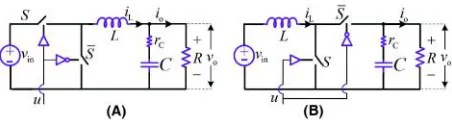
Figure 1 shows the schematic of a synchronous buck and boost DC-DC converters, where the gate signal ‘u’ is taken as the control variable. Under a PWM technique, the control technique adjusts the duty-ratio
d in order to regulate the output voltage of a DC-DC
converter to the desired value. Using the inductor
volt-second balance, the respective voltage gains of the buck and boost converters can be shown to be
d
and 1/(1-d) while operating under continuous conduction mode (CCM).Fixed-frequency Control
A fixed-frequency PWM-based approach remains a prevalent choice as it simplifies the design of the input filter. In a PWM scheme, the (switching) time period is fixed, and the on-time is accordingly adjusted by the feedback control loop. The voltage-mode and current-mode are the two popular PWM control schemes. Figure 2(A) shows a synchronous buck converter operating under a PWM voltage-mode control (VMC) scheme, and the related control waveforms are shown in Fig. 3. It uses a single-loop control architecture. The voltage controller Gc computes the control signal vc by taking the error voltage ve as input, where ve = vref - vo. The comparator output uc is generated by comparing vc with the periodic saw-tooth waveform with a time period Ts. The comparator follows a S-R latch circuit which is set by the rising edge of switching frequency clock Fs and reset by the comparator output uc. A dead-time circuit is used to avoid the shoot-through current using a synchronous configuration. Despite its simplicity and improved load regulation, a VMC technique suffers from poor line regulation and phase margin. An input voltage feed-forward can be used to improve the line regulation.
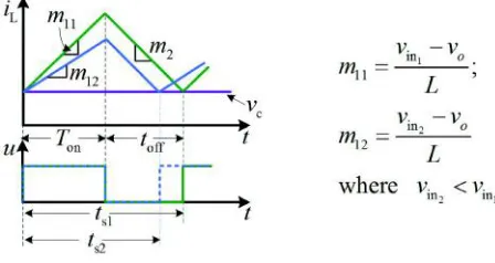
Figure 2(B) shows the schematic of a PWM CMC scheme which consists of two feedback loops. Here, the outer voltage-loop generates the reference command vc for the inner current-loop. It can be broadly categorized as peak CMC, valley CMC, and average CMC. Figure 4 shows the control waveforms using the peak and valley CMC schemes. In the former [shown in Fig. 4(a)], the control signal vc is compared with the peak value of the inductor current, whereas Fig. 1: Schematic of DC-DC converters: Synchronous (A)
[image:2.612.319.545.83.143.2]the valley point of the inductor current is compared with vc in the valley CMC as shown in Fig. 4(B). Any change in the input voltage vin would be immediately reflected via the inductor current; thereby, it can achieve superior line transient response and line regulation. However, it suffers from sub-harmonic instability when the duty-ratio D > 0.5and often requires an external ramp compensation for stabilization.
Variable-frequency Control
A variable-frequency control technique finds widespread applications in point-of-load converters because of its simplicity in implementation, fast
transient response, and improved light-load efficiency (Redl W R and Jian S, 2009). Based on their modulation, they can be broadly categorized as constant on-time, constant off-time, and hysteretic control modulations.
Constant on/off-time Control
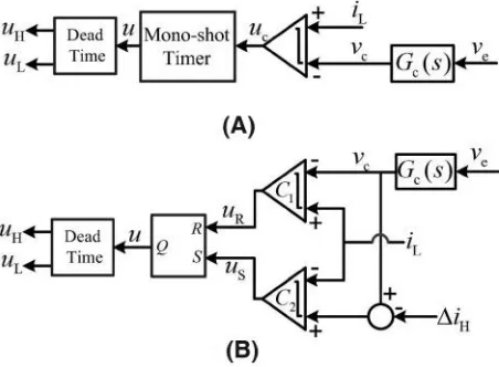
Figure 5(A) shows the schematic diagram of CMC Fig. 2: Schematic of a synchronous buck converter operating
under PWM (A) voltage-mode control and (B) current-mode control techniques
Fig. 3: Control waveforms under PWM voltage-mode control
Fig. 4: Control waveforms under PWM current-mode control: (A) peak CMC and (B) valley CMC
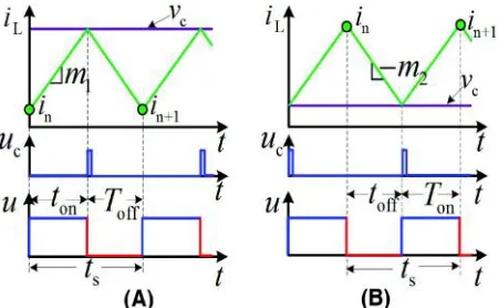
Fig. 5: Schematic diagram of a variable-frequency CMC (A) constant off-time modulation and (B) hysteretic mo dul ati on
[image:3.612.67.291.79.322.2] [image:3.612.317.546.83.184.2] [image:3.612.320.546.361.527.2] [image:3.612.100.265.381.504.2]mono-shot timer expires. The switch turns-off when
iL crosses vc [shown in Fig. 6(A)] and the mono-shot timer is triggered.
Similarly, the operation of a constant on-time scheme can be explained using Fig. 6(B). Here, the mono-shot timer is triggered when vccrosses iLand the controllable switch turns-on. Once the on-time expires, the high-side switch S turns-off. This modulation scheme can be useful to improve the light-load efficiency (Redl W R and Jian S, 2009).
Hysteretic Control
Figure 5(B) shows the schematic diagram of a current-mode hysteretic modulator, and the relevant control waveforms are shown in Fig. 7. In this modulation, the inductor current is kept within a specified band using the controller output and a hysteresis band. The output of the voltage controller
vcis used as the peak current reference, whereas the valley reference current is generated using vcand the hysteretic band iH as shown in Fig. 7. When the inductor current iLcrosses vc, the high-side switch turns-off, and it turns-on when iLfalls below the valley reference current (vc -iH).
Advantages and Shortcomings in Variable-frequency Control
The fixed-frequency peak CMC suffers from sub-harmonic instability when the operating duty-ratio D > 0.5 and it often requires an external ramp compensation for stabilization. This degrades the achievable closed-loop bandwidth. On the other hand, the current-loop of variable frequency CMC is inherently stable and shows improved closed-loop bandwidth; however, suffer from varying switching frequency.
Sub-harmonic Instability
Fixed-frequency Control : Figure 8 shows the control
waveforms under the PWM peak CMC scheme. The solid and dotted lines indicate the steady-state and perturbed waveforms. Let inand in+1 be initial and final values of the inductor current during the nth cycle.
Referring to Fig. 8, the current dynamics can be written as
n+1 n 1 s 2 1 s
i i m DT m D T (3.1)
where, m1 and m2 are the respective rising and falling slopes of the inductor current, and D is the steady-state duty ratio. From (3.1), the perturbed current dynamics can be written as
2
n+1 n
1
.
m i
m i
(3.2)
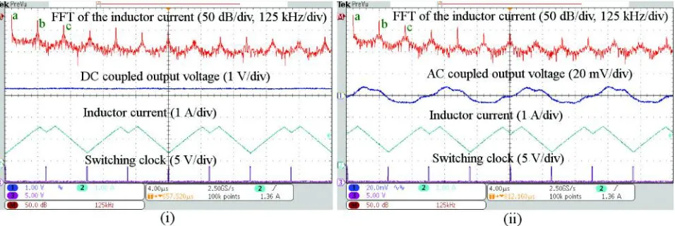
It can be shown from (3.2) that the current-loop under PWM peak CMC remains stable if the steady-state duty ratio D < 0.5. This fact is verified using test results in Fig. 9 for a buck converter using the parameter set: vin = 6V, vo= 3.3V, L = 10H, C =
150F, io= 1.5A and Fs = 200kHz. Here, a PWM peak CMC technique was implemented with the closed inner-loop and opened outer-loop and the steady-state duty-ratio was found to be D = 0.55. Under this condition, Fig. 9(i) demonstrates the existence of sub-Fig. 6: Control waveforms of a variable-frequency CMC (A)
constant off-time modulation and (B) constant on-time modulation
[image:4.612.68.293.83.222.2] [image:4.612.96.267.550.707.2]harmonic instability using the peak CMC, which is evident from the FFT trace with a sharp peak at 100~kHz for the switching frequency of 200~kHz.
Using an additional compensating ramp with a slope mc, the stability of the inner current-loop can be enhanced; the condition of current-loop stability can be derived as
2
2 c
n+1 n
c
.
m m
m m
i i
(3)
Using the above condition, Fig. 10 shows that the peak CMC technique can be stabilized using ramp compensation in a synchronous buck converter under the same operating condition as in Fig. 9. The FFT trace in Fig. 10 clearly shows that there is no sub-harmonic component in the power spectrum. Comparing the steady-state performances using the
unstable (in Fig. 9) and the stable (in Fig. 10) cases, one can infer that a sub-harmonic instability leads to a higher RMS value of the inductor current, which would result in higher conduction losses. Also the output voltage ripple significantly increases for the former compared to its nominal value as shown in the latter. Similarly for PWM valley CMC, it can be shown that the current stability can be ensured for the steady-state duty ratio D>0.5, which would also require a ramp compensation for stabilization when the operating duty-ratio D<0.5.
While the current-loop stability can be enhanced using a compensating ramp, it would degrade the closed-loop bandwidth; thereby, penalizing the transient performance (Ridley R B, 1991). Figure 11 shows the Bode plots of the control-to-output transfer function of a CCM buck converter under the PWM peak CMC using different ramp slopes. It is observed that an increase in the ramp slope decreases the closed-loop DC-gain and bandwidth, and a further increase in the ramp slope would tend to approach towards VMC; thus, the benefits of CMC would be lost.
Variable-frequency Control : Referring to the
waveforms using the current-mode constant off-time control technique as shown in Fig. 6(A), the inductor current at the end of nth cycle can be written as
n+1 c 2 off
i
v
m T
(3.4)Applying small perturbations, the perturbed Fig. 8: Perturbed and nominal control waveforms under
PWM peak CMC
[image:5.612.70.292.78.205.2] [image:5.612.69.547.528.688.2]current dynamics can be obtained as iˆn+1vˆc. This implies that the inner current-loop is inherently stable irrespective of the steady-state duty ratio and the overall closed-loop stability is determined by the outer voltage loop. Figure 12 shows the test results using the current-mode constant off-time modulator with the opened outer voltage-loop using the same test conditions as in Fig. 9. Figure 12 shows that the stable periodic behavior can be achieved for D>0.5 without the need of a ramp compensation using the current-mode constant off-time modulation. It is also evident
from the FFT trace of the inductor current. Stability of the inner current-loop can be retained for any arbitrary duty-ratio without using a compensating ramp. Similar stability results can be shown for a current-mode constant on-time control scheme.
Frequency Regulation
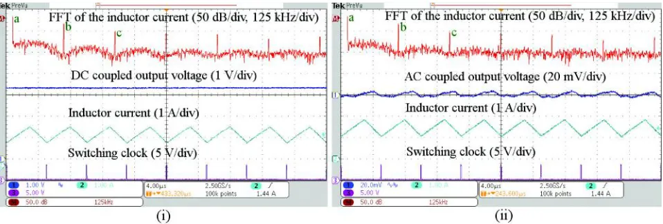
While a variable frequency CMC technique offers inherent current-loop stability over a PWM CMC technique, a variation in steady-state switching frequency remains a concern for the former, which makes it difficult to design an input filter using the Fig. 10: Steady-state waveform of a CCM buck converter under fixed-frequency peak CMC using ramp compensation with the outer voltage-loop open at 1.5 A load current and D=0.55; with (i) DC coupled output voltage and (ii) AC coupled output voltage; (a) DC component of the inductor current, (b) switching frequency (Fs) component, and (c) integer multiple of switching frequency (2*Fs) component; Time scale of 4 s/div
[image:6.612.68.547.82.244.2] [image:6.612.116.495.311.526.2]former (Redl W R and Jian S, 2009). Figure 13 shows the effect of input voltage variation on switching frequency for a constant on-time controlled buck converter. This technique is very sensitive to ambient noise (Redl W R and Jian S, 2009; Fang C C and Redl R, 2014; Fang C C, 2012). It can be noted from Fig. 13 that using the constant on-time, the steady-state switching frequency increases (or decreases) as the input voltage decreases (or increases). There exist various techniques to regulate the steady-state switching frequency either by adaptively varying the steady-state on-time (Qian T, 2013; Sahu B and Rincon-Mora G A, 2007; Lin H C et al., 2008) for constant on-time control, or by varying the off-time for constant off-time control or by varying the hysteretic band (Fu W et al., 2015) under hysteretic modulation. The method of constant on-time adaptation requires precise input voltage sensing either
by direct feed-forward (LM5017, 2015) or by estimation. The relation between the constant on-time
Ton and the input-voltage vin for constant on-time modulated buck converter is given as
o on
on s 2
in in in
1
v T
T T
v v v
However, for the sake of simplified analog implementation (LM5017, 2015), a piecewise linear approximation is used to relate the on-time and the input voltage to achieve a quasi-fixed frequency. However, this approximation leads to a wider frequency variation while operating over a wide range. There exist various methods for frequency regulation at steady-state, such as using analog phase-locked loop (PLL), delay-line PLL, digital PLL, etc.,(Jing X and Mok P K T, 2013; Li P et al., 2011). Such methods do not require any input voltage sensing, but can precisely regulate the switching frequency using an additional frequency-loop. These methods of frequency regulation require more hardware resources and exhibits slower locking time.
Need for Digital Implementation and Challenges
Recently, digital controllers have emerged as a viable alternative (Maksimovic D et al., 2004; Liu Y F et
al., 2009) due to their ease of integration with other
digital systems and ability to implement high-performance control schemes. Using a traditional controller-tuning method based on worst-case scenario, the closed-loop performance is often Fig. 12: Steady-state waveform of a CCM buck converter using constant off-time CMC with the outer voltage-loop open at 1.5 A load current and D=0.55; with (i) DC coupled output voltage and (ii) AC coupled output voltage; (a) DC component of the inductor current, (b) switching frequency (Fs) component, and (c) integer multiple of switching frequency (2*Fs) component; Time scale of 4s/div
[image:7.612.70.548.78.239.2] [image:7.612.66.290.312.431.2]compromised during the nominal operating conditions. A real-time (auto) tuning is a viable alternative, in which the gains are adaptively varied based on the operating conditions. Suitable gains can be computed either online or offline, and a look-up-table (LUT) based method can be used for digital implementation. Further, a digital platform simplifies the frequency regulation methods using an all-digital PLL (ADPLL) with a time-to-digital converter (TDC). A TDC captures the instantaneous switching period Ts,n and accordingly adjusts the desired timing parameter using
Tc,d = (Tc/Ts,n)*Ts,d where Tc is the instantaneous constant-time and Ts,d is the desired switching period (1/ Fs). This can be programmed in a digital device which also offers the flexibility of controller tuning and (constant) time adaptation (band adaptation in the case of hysteretic modulator) and speed-up the frequency locking mechanism within a few switching cycles.
Digital Implementation
Figure 14 shows the schematic diagram of a synchronous buck converter operating under the mixed-signal constant on-/off-time CMC scheme, where iL, vo and vref indicate the inductor current, the output voltage, and the reference voltage, respectively. The output voltage vois sampled using a uniform clock
Fvs(may be the same rate of the switching frequency
Fs or higher) using an analog-to-digital converter (ADC). Using the error voltage ve[n] (=vref –vo[n]), the digital voltage controller Gc(z) computes the control signal vc[n] at the rate of sampling clock Fvs. In fully digital current-mode control (DCMC), the inductor current is also sampled and taken to the digital domain using a high speed ADC. Instead, in mixed-signal DCMC (Saggini S et al., 2004; Trescases O et al.,
2011) the inductor current is placed in the analog domain and the control signal vc[n] in digital domain is converted to analog domain using a digital-to-analog converter (DAC). The analog control signal vA is then compared with the sensed inductor current
i
Lusing a high speed analog comparator. As shown in Fig. 14, the comparator output uc triggers the mono-shot timer for constant on-/off-time mode of operation. Followed by it is the ‘dead-time circuit’ which generates the respective gate signals for the synchronous mode of operation.Limit Cycle Oscillation
Although the variable frequency control offers many advantages over fixed-frequency control, the choice of sampling frequency in a variable-frequency digital modulator still remains a challenge, which is because of the mismatch in the switching and the sampling points. Figures 15 and 16 demonstrate the experimental results of the synchronous buck converter operating under mixed-signal constant off-time CMC scheme. The converter is designed to operate with the nominal switching frequency of 200 kHz and with an output voltage of 3.3 V. The output voltage is sampled at the same rate of the switching frequency. As shown in Fig. 15, there exists a fast-scale instability which is often known as multi-limit cycle instability (Krein P T and Bass R M, 1989). This increases the inductor current ripple, thereby increasing the conduction losses. If the sampling
Fig. 14: Schematic of the synchronous buck converter under the variable frequency mixed-signal constant on-/ off-time CMC scheme
[image:8.612.317.546.503.665.2] [image:8.612.68.294.582.701.2]frequency is increased to 5 times the switching frequency (Fvs = 5* Fs), the current ripple is reduced, but instability still persists as shown in Fig. 16.
Non-uniform Sampling in Variable-frequency Control
Figure 17 shows the schematic diagram of a synchronous buck converter operating under the mixed-signal current-mode constant on/off-time control using an event-based sampling approach (Hariharan K et al., 2016). The output voltage vois sampled using a non-uniform clock Fvswhich uses the rising edge of the high-side gate signal uHfor the constant off-time control and the falling edge of uH for the constant on-time control. The digital voltage controller Gc(z) takes the sampled error-voltage ve and computes the control signal vc using Fvs. The rest of the operation is similar to the digital implementation part given in Section Digital Implementation.
Discrete-time Modeling
A traditional state-space averaging method fails to capture fast-scale instability as this approach ignores the ripple information. On the other hand, the discrete-time model (Verghese G C et al., 1986) predicts the fast-scale instability and also enables one to design a controller directly in digital domain. Referring to Fig. 18, a general discrete-time model of a CCM buck converter can be written as
n+1 n, n ; n+1 n, n ,
i f i v v g i v
where, in and vn are the inductor current and the output voltage at the beginning of the nthcycle, and i
n+1 and
vn+1represent their respective values at the end of the same cycle. Referring to Fig. 18, the modeling is carried out in two steps: in step 1, i1 and v1are obtained when the high-side switch is turned off. Subsequently, in step 2, in+1 and vn+1 are obtained; thereby, the complete discrete-time model can be obtained, in which the final values in+1 and vn+1can be obtained in terms of their initial values in and vnduring the nth
cycle. Fig. 16: Steady state waveform of a CCM buck converter
using mixed-signal constant off-time CMC scheme at 1.5 A load current with kp = 7.5 and kp = 0.3 using uniform sampling with Fvs = 5*Fs = 1 MHz; constant off-time Tc = 2.03s; FFT traces shows the spectrum of the inductor current; Time scale of 8 s/div
Fig. 17: Schematic of a mixed-signal current-mode constant on-/off-time modulator using an event-based sampling approach (Hariharan K et al., 2016)
Fig. 18: Control waveform of the general discrete-time mo de l
Discrete-time Modeling Under an Event-driven Control Scheme
The state-space model of a synchronous buck converter is given by
0 1 in 1 1 , o o
A A Bv u A u v C
x x x x x
(5.1)
[image:9.612.68.295.79.246.2] [image:9.612.322.545.274.336.2] [image:9.612.352.515.393.523.2]0
n
0 0
; 0
A
R RC
1 / ;
0
L B
L n C
n1
n
/ /
/ 0 ;
r R r L R L
A
R C
Co
R rn C Rn
;
n / C
R R Rr and the control input u = 1 for the
mode 1 (uH = 1, uL = 0) configuration and for mode 2 (uH = 0, uL = 1) configuration, the control input u = 0. Similar to the discrete-time models derived for the digital current hysteresis control using an event-driven sampling clock (Kapat S, 2017), and the stability criterion for constant on-/off-time modulation was found to be
C C 1p i
C C
1
1 1
2
r T
r R
k
r C k
(5.2)
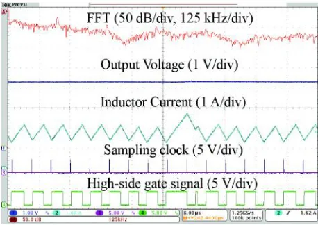
where, kp and ki are the proportional and integral gains and Tcis the constant-time parameter. From (5.2), it can be concluded that the stability boundary can be further enhanced by decreasing the ESR of the output capacitor. Figure 19 demonstrates the experimental results of a CCM buck converter under the mixed-signal constant off-time control CMC scheme using the event-based sampling approach. An event-based sampling method can completely eliminate the limit-cycle oscillation and achieve stable periodic behavior.
This is evident from the inductor current FFT traces shown in Fig. 19.
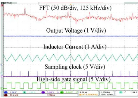
For constant on-time modulation, the same stability boundary in (5.2) can be used with Tc as the constant on-time. Figure 20 demonstrates the experimental results of a CCM buck converter under the mixed-signal constant on-time CMC scheme using an event-based sampling approach. The event-based method of sampling the output voltage at the falling edge of the high-side gate signal completely eliminates the limit-cycle oscillation behavior and achieves stable periodic behavior. This is evident from the inductor current FFT traces shown in Fig. 20.
A Controller Design Case Study Using Current-mode Constant Off-time Modulation
The feedback voltage controller using the current-mode constant on-time and/or off-time modulation techniques can be designed using discrete-time small-signal models. Consider a case study under the current-mode constant off-time modulation with the objective to achieve 45ophase margin and 10 kHz
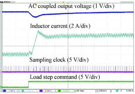
closed-loop bandwidth using a PI voltage controller. Following the modeling approach (Kapat S, 2017), the discrete-time controller gains are found to be kp = 8 and kp = 0.3. Figure 21 shows the transient response of the synchronous buck converter for a step change in load current from 1.5 A to 6 A using the mixed-signal current-mode constant off-time scheme. The Fig. 19: Steady-state waveform of a CCM buck converter
under the mixed-signal constant off-time CMC scheme at 1.5 A load current with kp = 7.5 and kp = 0.3 using an event driven sampling; constant off-time Tc = 2.03s; FFT traces shows the spectrum of the inductor current; Time scale of 8s/div
[image:10.612.68.296.83.245.2] [image:10.612.317.546.498.662.2]figure shows that 128s settling time and 600 mV (output voltage) undershoot are achieved.
The performance can be further improved by further increasing the proportional gain; however, this would increase the peak (inductor) current. While this is acceptable if the inductor current stays within its current limit, this would also increase the on-time duration of the high-side MOSFET for faster slew-up, thereby increasing the sampling interval using this event-based sampling approach. Due to the unavailability of output voltage samples during this slew-up process, the voltage controller fails to update, which may result in a complete collapse of the closed-loop system. This can be avoided by incorporating an additional uniform sampling clock which needs to be time-multiplexed with the event-based sampling clock, in which the latter is used throughout and the former would be only used when the inter-sample duration exceeds a threshold value. With this arrangement, a variable frequency digital/mixed-signal current mode controller can be designed to meet a high bandwidth demand over a wide operating range. Here, unlike in a PWM CMC technique, a ramp-compensation is not needed for current-loop stability while operating over a wide duty-ratio range; thus the benefits of current-mode control can be retained without compromising the current-loop bandwidth.
While the objectives in this paper are to highlight the benefits of using variable frequency digital current-mode control over its fixed-frequency counterpart, the relevant discussions are equally applicable for the given application needs. Then all the design guidelines are equally applicable, and the salient features would be retained. It is important to note that the benefits would be more pronounced for higher and/or lower duty-ratio operating regions. For any specific application, the following steps may be considered:
i) The power circuit needs to be designed first.
ii) Using power circuit parameters, the effective
sampling frequency and the nominal timing parameters need to be designed.
iii) The digital voltage controller can then be designed to meet the steady-state and closed-loop transient performance requirements.
Conclusions
In this paper, the merits and demerits of both the fixed-frequency and the variable-fixed-frequency control techniques were highlighted for DC-DC converters. It was found that the variable-frequency control would achieve inherent current-loop stability over a wide range of duty-ratio without the need of an additional compensating ramp. The steady-state switching frequency can be precisely regulated using an all-digital PLL. Further, a all-digital controller can be tuned for further performance improvement. An event-driven sampling mechanism would be very useful to overcome multi-limit cycle oscillations. Thus, such techniques emerge as an attractive digital control solution for future power management applications. Fig. 21: Transient response of a synchronous buck converter
under the current-mode constant off-time technique using an event-based sampling approach for the load step-up from 1.5 A to 6 A with the controller gains kp = 8 and ki = 0.3; Time scale of 40s/div
References
Fang C C (2012) Closed-form critical conditions of instabilities for constant on-time controlled buck converters IEEE
Transactions on Circuits and Systems I 59 3090-3097
Fang C C and Redl R (2014) Subharmonic stability limits for the
buck converter with ripple-based constant on-time control and feedback filter IEEE Transactions on Power Electronics 29 2135-2142
adaptive minimum-on-time control for low-power microcontrollers IEEE Transactions on Power Electronics 31 418-429
Hariharan K, Kapat S and Mukhopadhyay S (2016) Unified constant on/off-time hybrid compensation for fast recovery in digitally current-mode controlled point-of-load converters in Proc IEEE APEC 315-321
Hsieh H, Li J and Chen D (2008) Effects of X capacitors on EMI filter effectiveness IEEE Transactions on Industrial
Electronics 55 949-955
Jing X and Mok P K T (2013) A fast fixed-frequency adaptive-on-time boost converter with light load efficiency enhancement and predictable noise spectrum IEEE Journal
of Solid-State Circuits 8 2442-2456
Kapat S (2016) Reconfigurable periodic bifrequency DPWM
with custom harmonic reduction in DC–DC converters IEEE Transactions on Power Electronics 31 3380-3388
Kapat S (2017) Parameter-insensitive mixed-signal hysteresis-band current control for point-of-load converters with fixed frequency and robust stability IEEE Transactions on Power
Electronics 32 5760-5770
Krein P T and Bass R M (1989) Multiple limit cycle phenomena in switching power converters in Proc IEEE APEC 143-148
Lakshminarasamma N and Ramanarayanan V (2007) A family of
auxiliary switch ZVS-PWM DC–DC converters with
coupled inductor IEEE Transactions on Power Electronics 22 2008-2017
Li J, Qiu Y, Sun Y, Huang B, Xu M, Ha D S and Lee F C (2007) High resolution digital duty cycle modulation schemes for voltage regulators in Proc IEEE APEC 871-876
Li P, Bhatia D, Xue L and Bashirullah R (2011) A 90-240 MHz hysteretic controlled DC-DC buck converter with digital phase locked loop synchronization IEEE Journal of
Solid-State Circuits 46 2108-2119
Lin H C, Fung B C and Chang T Y (2008) A current mode adaptive on-time control scheme for fast transient DC-DC converters in Proc IEEE ISCAS 2602-2605
Liu Y F, Meyer E and Liu X D (2009) Recent developments in digital control strategies for DC/DC switching power converters IEEE Transactions on Power Electronics 24 2567-2577
LM5017 (2015) 100-V, 600-mA Constant on-time synchronous buck regulator Texas Instruments
Maksimovic D, Zane R and Erickson R (2004) Impact of digital control in power electronics in Proc IEEE ISPSD 13-22
Qian T (2013) Subharmonic analysis for buck converters with constant on-time control and ramp compensation IEEE
Transactions on Industrial Electronics 60 1780-1786
Redl W R and Jian S (2009) Ripple-based control of switching
regulators–an overview IEEE Transactions on Power Electronics 24 2669-2680
Ridley R B (1991) A new, continuous-time model for current-mode control IEEE Transactions on Power Electronics 6 271-280
Saggini S, Ghioni M and Geraci A (2004) An innovative digital control architecture for low-voltage high-current DC-DC converters with tight load regulation IEEE Transactions
on Power Electronics 19 210-218
Sahu B and Rincon-Mora G A (2007) An accurate, low-voltage, CMOS switching power supply with adaptive on-time pulse-frequency modulation (PFM) control IEEE
Transactions on Circuits and Systems I 54 312-321
Trescases O, Prodic A and Ng W T (2011) Digitally controlled current-mode DC-DC converter IC IEEE Transactions on
Circuits and Systems I 58 219-231
Tse K K, Chung H S-H, Hui S Y R and So H C (2002) A comparative study of carrier-frequency modulation techniques for conducted EMI suppression in PWM converters IEEE Transactions on Industrial Electronics 49 618-627
Verghese G C, Malik M E and Kassakian J G (1986) A general approach to sampled-data modeling for power electronic circuits IEEE Transactions on Power Electronics PE-1 76-89
Yan Y, Lee F C and Mattavelli P (2012) Unified three-terminal switch model for current mode controls IEEE Transactions
on Power Electronics 27 1965-1972
Yan Y, Lee F C and Mattavelli P (2013) Comparison of small signal characteristics in current mode control schemes for point-of-load buck converter applications IEEE