1
Faculty of Electrical Engineering,
Mathematics & Computer Science
Interference Nulling via a
Resistor-Weighted Op-Amp
Vector Modulator
Frederik van den Ende Master of Science Thesis
March 2011
Supervisors
Abstract
In order to perform interference nulling (through beamforming), for an in-terferer with variable angular position, the radiation pattern of an array antenna has to be adjusted electronically.
This thesis deals with a beamforming algorithm that rotates the beams of a Butler Matrix beamforming network (BFN), such that one of the beams is able to ’capture’ an interferer. This beam is strongly attenuated, such that the interferer is nulled out. In this way the signal-to-interference ratio (SIR) is improved. Subsequently, a vector modulator performs phase shifting in order to optimize the signal-to-noise ratio (SNR).
Based on an existing platform, a circuit level implementation, using Op-Amps and resistors, is proposed to verify the nulling performance of the beamforming algorithm.
Contents
1 Introduction 1
1.1 Beamforming . . . 2
1.1.1 Antenna Array Basics . . . 2
1.1.2 Complex Weights . . . 3
1.2 Project Description . . . 3
1.3 Previous Work . . . 4
1.4 Idea . . . 5
1.5 Research Questions . . . 5
1.6 Acknowledgements . . . 6
1.7 Outline . . . 6
2 Interference Nulling 7 2.1 Multiple Beams . . . 7
2.2 Butler Matrix . . . 7
2.3 Motivation for the Butler Matrix . . . 9
2.4 Analysis of the Butler Matrix . . . 10
2.4.1 Beam Position . . . 10
2.4.2 Phase Progression . . . 11
2.4.3 Matrix Synthesis & Orthogonality . . . 11
2.5 Beam Summation. . . 13
2.6 Beam Cancellation . . . 14
2.7 Broadside Butler . . . 15
3.1 Howells-Applebaum Algorithm . . . 19
3.2 Synthesis of the Complex Weights . . . 21
3.3 2-Step Beamforming . . . 23
3.3.1 Beam Weighting . . . 23
3.3.2 SNR Optimization . . . 25
4 Beamforming Platform 27 4.1 System Functions . . . 27
4.2 Motivation . . . 28
4.2.1 Mixer Array. . . 29
4.2.2 TIA Stages . . . 29
4.2.3 Linearity . . . 30
5 System Model Evaluation 31 5.1 Circuit Constraints . . . 31
5.1.1 Butler Beamforming Network . . . 31
5.1.2 Weight Quantization . . . 32
5.2 Model Simulations . . . 32
5.2.1 Quantized Butler Phases. . . 32
5.2.2 Quantized Magnitude Weights . . . 34
5.2.3 Quantized Phase Weights . . . 34
6 Circuit Level Design 37 6.1 Beamforming Front-End . . . 37
6.2 Mixer Block . . . 38
6.3 Butler BFN . . . 39
6.4 TIA Stage . . . 40
6.4.1 Proposed Circuit Implementation . . . 40
6.4.2 Transimpedance . . . 41
Contents
6.4.4 Charge Pump . . . 42
6.4.5 Bandwidth . . . 43
6.5 Vector Modulator . . . 43
6.5.1 Vector Modulation . . . 44
6.5.2 Synthesis of the Weights . . . 45
6.5.3 Implementation of the Weights . . . 46
6.5.4 Proposed Vector Modulator Implementation. . . 47
7 Simulation Results 49 7.1 Simulation Setup . . . 49
7.2 Gain Compression . . . 50
7.3 Third-Order Intermodulation Distortion . . . 51
7.4 Vector Modulator . . . 52
7.5 Nulling Performance . . . 53
7.6 A Word about Noise . . . 54
7.7 Power Consumption . . . 54
8 Conclusions 55
9 Recommendations 57
Chapter 1
Introduction
Nowadays the radio-frequency (RF) spectrum becomes increasingly filled with transmitters operating in the same frequency-band. Modern radio re-ceivers need to support a variety of (mobile) communication standards, each using a different frequency-band. Due to this ’crowded’ spectrum, receivers need to accommodate quite a few highly selective analog filters in order to select the right frequency-band.
High-order analog filters typically operate in a single fixed frequency-band. This is undesired for upcoming applications, such as software-defined radio (SDR) and cognitive radio (CR), which require a high degree of flexibility. Cognitive radio operates in unused spots in the frequency spectrum. Fixed transmitters (e.g. TV channels) are closely spaced to these empty spots and are considerably stronger. Strong interferers, nearby the wanted signal (band), are hard to reject by means of frequency-domain filtering. Still, these blocking signals or blockers can desensitize the receiver.
Consider Figure 1.1where a piece of unused spectrum (between two strong interferers) is available for cognitive radio applications. A band-pass filter might be used to select this ’piece of spectrum’.
f
Unused Spectrum
Although the interferers are located outside the passband of this filter, they cannot be suppressed adequately, due to the finite steepness of the band filter. Therefore another approach should be exploited, in order to reject these kind of strong interferers.
1.1
Beamforming
Antennas can be configured as an array of antenna-elements. When the signals from these elements are amplified and/or phase-shifted and subse-quently summed, the radiation pattern is modified. In this way the radiation pattern of the array can be adjusted electronically. This is called beamform-ing. Beamforming is also referred to as spatial filtering. If, as in the case
of Figure 1.1, a wanted signal and an interferer are spatially separable, it might be possible to obtain sufficient rejection. Beamforming can also be used in order to increase the signal-to-noise ratio (SNR).
1.1.1 Antenna Array Basics
Consider a linear array ofK omnidirectional equally spaced radiators. It is
assumed that the radiators have an isotropic radiation pattern and mutual coupling between the elements is neglected for simplicity. Consequently, the radiation pattern of the array is described by the array factor (F) [Visser,
2005, p. 127], that is:
F(θ) =
K
X
i=1
ejk0(i−1)dsin(θ) (1.1)
where
k0= 2π λ0
• λ0 is the wavelength in free space.
• k0 is the angular wave number in free space, i.e. the magnitude of the wave vector.
• d is the inter-element distance.
• θis the angle relative to the array normal (broadside or z-direction).
So, when the contributions from the elements are summed, the radiation pattern of the array is obtained. In Figure 1.2b the radiation pattern of a 4-element linear array with 1
1.2. Project Description
(a) Array configuration
−50 0 50
−40 −30 −20 −10 0 10
θ [°]
F(
θ
) [dB]
(b) Radiation pattern
Figure 1.2: Configuration and radiation pattern of a 4-element linear array.
The radiation pattern is plotted for θ = [−90◦. . .90◦], i.e. visible space, because the array factor for the interval θ= [90◦. . .270◦] is mirrored with respect to the intervalθ= [−90◦. . .90◦].
1.1.2 Complex Weights
In the expression for the array factor (1.1), it is assumed that the amplitudes received by the elements of the array are equal. That is, the array exhibits a uniform aperture distribution. It is also assumed that the summation network introduces no additional phase differences or time delays.
Most array systems incorporate ’weights’ in order to perform beamforming. These weights can provide amplification and/or phase shifting. Hence the namecomplex weights. Amplitude weighting is often referred to asamplitude tapering [Visser, 2005,§4.6]. An amplitude taper lowers the sidelobe level
at the cost of broadening the main beam. Phase tapers are used to phase
shift the antenna signals such that they coherently add up. In this way, the SNR can be improved for a certain direction of arrival, as in the case of a
Phased Array.
1.2
Project Description
This thesis examines the feasibility of implementing a beamforming system to perform interference nulling. This work is performed in the framework
of beamforming for consumer electronics, i.e. personal communications for frequencies of 1 - 5 GHz.
1.3
Previous Work
In previous work [Soer et al.,2011], a beamforming system based on a Vec-tor ModulaVec-tor was proposed. A vector modulator performs phase
shift-ing and/or amplification, by modulatshift-ing the magnitudes of two quadrature phases (orthogonal vectors) and summing the results.
Consider Figure 1.3. Summing two orthogonal vectors, i.e. I & Q, yields the resulting vector, which experiences a phase shift with respect to I & Q. In this way the complex weights can be adjusted in order to steer a beam to a desired direction.
I Q
Figure 1.3: Phasor Diagram.
[Wang and Hajimiri,2007] presented a digital linearPhase Rotator, in which
the I & Q components of the local oscillator (LO) signal each serve as input to a variable gain amplifier (VGA). These VGAs are transconductor stages, sensing the LO signal and producing an output current. Their gains are 5 bit digitally controlled and can be set independently from each other. Adding the outputs of the VGAs in the current domain results in an interpolated signal with the desired phase and amplitude.
[Raczkowski et al., 2010] reported a wideband beamformer, in which the output currents of a quadrature mixer serve as input to a phase shifter. These phase shifters are implemented using 4 digitally controlled variable-gain current amplifiers, as currents are easily summed to produce the phase-shifted output signal. The phase shifts are derived from a lookup table, which contains the gains of a single VGA.
The complex weights of the beamforming system proposed by [Soer et al.,
1.4. Idea
1.4
Idea
In this work the implementation of complex weights based on the combi-nation of Op-Amps and resistors is examined. This could save power
con-sumption and die area compared to using capacitors as in [Soer et al.,2011]. Consider Figure 1.4.
R
IR
QR
FB VIVQ
VOUT
Figure 1.4: Possible implementation of a Vector Modulator.
The voltages VI & VQ, which are 90◦ out of phase (i.e. I/Q signals), are
converted to current through the variable resistors and added at the summa-tion node at the inverting input of the Op-Amp. Subsequently the summed current flows through the feedback resistor (RF B) and hence converted back
to voltage. So the resulting voltage (VOU T) experiences a phase shift with
respect to the input voltages. In this way a vector modulator can be con-structed.
This work examines if the implementation of complex weights, using resistors and Op-Amps, is suitable for a beamforming algorithm in order to perform interference nulling. This leads to the following research questions.
1.5
Research Questions
1. Given a linear phased array configuration, can the radiation pattern be adjusted in a structured way to perform interference nulling (with sufficient accuracy) through beamforming?
1.6
Acknowledgements
First of all, I would like to thank Michiel Soer for providing me with this assignment. It was challenging & versatile, ranging from array theory to pat-tern synthesis and from front-end design considerations to Op-Amp circuits. Also his help considering circuit simulations is acknowledged.
Secondly, I would like to thank Eric Klumperink for his feedback on behalf of writing this thesis and the discussions considering the circuit implemen-tations. Also I want to thank Remko Struiksma for his critical review of this report. I would like to thank professor Bram Nauta, for facilitating this graduation project carried out within the ICD group of the University of Twente and professor Frank van Vliet for leading the graduation com-mittee. Furthermore I want to thank the (former) ICD students, especially Michiel Duiven for the nice cooperation during our studies.
My thank goes out to my parents, who gave me the opportunity to study and supported me during my whole study period. Finally I would like to thank Inge van Leeuwenkamp for her love and patience during the last months.
1.7
Outline
This thesis is organized as follows:
• Chapter 2 introduces a beamforming network (BFN), which is used to
perform interference nulling in a structured way.
• Chapter 3 describes a beamforming algorithm, which performs
inter-ference nulling and SNR improvement.
• Chapter 4 examines an existing platform for the beamforming system. • Chapter 5 evaluates the performance of the system model, due to
constraints imposed by a circuit implementation.
• Chapter 6 proposes circuit implementations, suitable for synthesizing
the complex weights of the beamforming system.
• Chapter 7 provides simulation results, obtained with SpectreRF. • Chapter 8 presents the conclusions.
Chapter 2
Interference Nulling
2.1
Multiple Beams
As elucidated in Chapter 1, the main function of the beamforming system is to perform interference nulling. It is hereby assumed, that the angular position of the interferer, which is random, is known a priori. However, in the absence of interference the array should be sensitive in all directions. As depicted in Figure 1.2b, the array is most sensitive in broadside direction (i.e. 0◦), whereas in endfire direction (i.e. ±90◦) the array is not sensitive at all. The four-element array has natural pattern nulls at ± 30◦. If an incoming signal enters the array at an angle of± 30◦ or ± 90◦, the array
will not notice its presence.
In order to satisfy these sensitivity conditions, multiple beams are needed.
Multiple beams can be created by means of a beamforming network (BFN) or via quasi-optical lenses [Hansen, 2009, §10.2]. The latter is not further
described here. The next section introduces an often used BFN.
2.2
Butler Matrix
A Butler Matrix1, named after his inventor [Butler and Lowe, 1961], is a
beamforming network, which can mathematically be represented by a square matrix:
0◦ −45◦ −90◦ −135◦
−90◦ 45◦ 180◦ −45◦
−45◦ 180◦ 45◦ −90◦ −135◦ −90◦ −45◦ 0◦
(2.1)
1
In Figure2.1an often encountered representation of a Butler BFN is given [Litva and Lo,1996,§2.2] [Rajagopalan,2006].
0° -90°
0° -90° A1 A2 A3 A4
1R 2L 2R 1L 45° 45°
Figure 2.1: Antenna array feeding a Butler BFN.
The BFN in Figure 2.1 consists of 4 hybrid junctions and 2 fixed phase shifters. A 4-element array antenna feeds the upper hybrid junctions, which perform a -90◦ phase shift when a signal propagates to the other branch in the hybrid. The outputs of the lower hybrids are referred to asbeam ports.
A Butler BFN connects N = 2n (where n = 1,2,3, . . .) array elements to
an equal number of beam ports. The signals present at these beam ports represent a beam. The Butler BFN in Figure2.1results 4 beams, which are shown in Figure2.2.
1 2 3 4 30
210
60
240
90 270
120 300
150 330
180 0
(a) Butler rosette
−50 0 50
−30 −20 −10 0 10
Magnitude [dB]
θ [°]
1R 2L 2R 1L
(b) Radiation pattern
Figure 2.2: Butler beams.
2.3. Motivation for the Butler Matrix
A Butler BFN is often recognized as the calculation flowchart (a.k.a. FFT butterfly) of the fast Fourier transform (FFT) [Hansen, 2009, §10.2.1.2]
[Mailloux, 2005, §1.3.2]. From this point of view, it could be said that a
Butler BFN performs a spatial fast Fourier transform. That is, the Butler
BFN performs an FFT on a discrete number of antenna elements, giving a discrete number of ’direction of arrival’ bins.
2.3
Motivation for the Butler Matrix
Next to the Butler Matrix in the general sense, there exists other types
of beamforming networks, such as the Blass Matrix and the Nolen Matrix
[Hansen,2009,§10.2.1.3]. A ’classical’ Blass matrix BFN uses a set of
array-element transmission lines, which intersect a set of beam port lines via power dividers to generate multiple beams. The Blass matrix BFN can have a number of beam ports unequal to the number of antenna elements.
The Nolen matrix BFN is in fact a generalization of both the Butler and the Blass matrices, such that the Nolen matrix can be reduced to the Butler matrix when N = 2n. Just like the Butler BFN can be considered an implementation of the FFT, the Nolen matrix BFN can be considered an implementation of the discrete Fourier transform (DFT).
So, more types of beamforming networks exist. Why not use those?
• A Butler BFN generates beams, which cover the complete visible space
of the array (in case of 1
2λspacing).
• As already mentioned above, the Butler BFN can be considered as an
implementation of the FFT. Hence it can be expected that this BFN requires a minimum number of components. Compared to the Butler BFN in Figure2.1, a Nolen matrix BFN would require 6 phase shifters & 6 hybrids for a 4-element array.
• A Butler BFN can be implemented using switches driven by different
phases. So it is suitable for implementation in CMOS, which offers good switches.
2.4
Analysis of the Butler Matrix
In this section the mathematical representation of the Butler BFN is ad-dressed. For clarity, Figure2.3visualizes the (direct) relation of the matrix with the beamforming network. Each box (Bi,j) represents a phase shift
corresponding to the elements of the matrix.
B1,1 B2,1 B3,1 B4,1 B1,2 B2,2 B3,2 B4,2 B1,3 B2,3 B3,3 B4,3 B1,4 B2,4 B3,4 B4,4
1R 2L 2R 1L
A1 A2 A3 A4
Figure 2.3: Direct implementation of the Butler matrix.
Radiation patterns, such as Figure1.2b, are often plotted as function of the variable u. Commonly referred to as u-space. The relation of u with the
angular variableθ is described by:
u= sin(θ)
In array theory it is customary to describe the mathematics in u-space, since beamwidth is invariant in u-space [Visser,2005,§7.2]. In addition, the phase
term in expression (1.1) becomes linear with u.
2.4.1 Beam Position
In u-space, the beams of a Butler matrix are located at [Hansen, 2009, p. 346] [Mailloux,2005, p. 392]:
ui =
iλ
2N d (2.2)
for
i=±
(
1,3,5, . . . ,(N −1) when N is even 0,2,4, . . . ,(N −1) when N is odd
So, in case of 1
2λspacing and a 4x4 Butler matrix, (2.2) simplifies to: ui =
i
2.4. Analysis of the Butler Matrix
In u-space, the 4 beams (i.e. N is even) are located at:
u=
−0.75 wheni=−3 −0.25 wheni=−1
0.25 when i= 1 0.75 when i= 3
(2.4)
2.4.2 Phase Progression
The phase progression between the elements of the matrix (i.e. Bi,j) is
described by [Mailloux,2005, p. 392]:
δi =−
i
Nπ (2.5)
In words, δi represents the increase/decrease in phase with respect to the
previous row-element of the matrix. For N = 4 and i = 1 the phase pro-gression becomes:
δ1=− 1
4π (2.6)
2.4.3 Matrix Synthesis & Orthogonality
With the aid of (2.6), the first row of the matrix (i.e. B1,j) can be
con-structed. Starting from broadside direction (i.e. ej0π) the row-elements become:
h
ej0π e−j14π e−j 1 2π e−j
3 4π
i
The second row of the matrix should contain the phases necessary to create a beam ’orthogonal’ to the first beam (1R). Orthogonal, meaningin geometric sense (perpendicular).
In Figure2.4the beams, at the positions given by (2.4), are represented by four impulses. For i= 1 expression (2.4) resulted a beam at u = 0.25. In order to be orthogonal with 1R, the second beam should be ±90◦ out-of-phase with the first beam. In u-space this corresponds to:
u= sin(±90◦) =±1 (2.7)
Figure 2.4: Beams located in u-space.
For u = −0.75 it follows from (2.4) that i = −3. From (2.5) the phase
progression for the second row of the matrix is:
δ−3 =−−3
4 π= 3
4π (2.8)
Again, starting from broadside direction, the row-elements become:
h
ej0π ej34π e−j12π ej14πi
In a similar way the phase progression fori= 3 andi=−1 result the phases
of the third and fourth row. Hence the Butler matrix becomes:
B =
ej0π e−j14π e−j 1 2π e−j
3 4π
ej0π ej34π e−j 1 2π ej
1 4π
ej0π e−j34π ej 1 2π e−j
1 4π
ej0π ej14π ej12π ej34π
(2.9)
The Butler beams can be calculated as:
1R 2L 2R 1L =
ej0π e−j14π e−j12π e−j34π
ej0π ej34π e−j 1 2π ej
1 4π
ej0π e−j34π ej 1 2π e−j
1 4π
ej0π ej14π ej 1 2π ej
3 4π A1 A2 A3 A4 (2.10)
A represents the element signals of the array. A multiplication with B,
results the phases - apart from a rotation - as defined in (2.1).
2.5. Beam Summation
2.5
Beam Summation
The beams generated by the Butler BFN can be summed in order to form a radiation pattern P(u):
P(u) =
1 1 1 1
1R 2L 2R 1L
(2.11)
Figure2.5illustrates the summing operation. The Butler BFN is represented by a black box, which could contain an implementation as illustrated in Figure 2.1.
Σ
Butler Matrix BFN
A1 A2 A3 A4
1R 2L 2R 1L
P
Figure 2.5: Summing the Butler beams yields the radiation patternP.
The beams, formed by the BFN in Figure2.1, are generated from the element signals as:
1R=A16 0◦ +A26 −45◦+A36 −90◦+A46 −135◦ (2.12a) 2L=A16 −90◦ +A26 45◦ +A36 180◦ +A46 −45◦ (2.12b) 2R=A16 −45◦ +A26 180◦ +A36 45◦ +A46 −90◦ (2.12c) 1L=A16 −135◦+A26 −90◦+A36 −45◦+A46 0◦ (2.12d) Summing these beams according to (2.11), results the radiation pattern shown in Figure 2.6a. Summing the beams, given by (2.10), yields the radiation pattern shown in Figure 2.6b. This Figure shows that different implementations of the Butler matrix represent the same Butler beams. However, when these beams are summed according to (2.11), the resulting radiation patterns (P) differ!
−1 −0.5 0 0.5 1 −30 −20 −10 0 10 Magnitude [dB] u−space
1R 2L 2R 1L P
(a) Using beams of (2.12)
−1 −0.5 0 0.5 1
−30 −20 −10 0 10 Magnitude [dB] u−space
1R 2L 2R 1L P
(b) Using beams of (2.10)
Figure 2.6: Radiation patterns of summed Butler beams.
2.6
Beam Cancellation
A Butler BFN distributes the received signal power of the array equally over its beam ports to form orthogonal beams. As depicted in Figure2.2b, the angle where one of the beams is at its maximum, the other beams are zero. As an example, consideru= 0.25, where the element signals are given by:
A=
ej0π
ej14π
ej12π
ej34π
(2.13)
At u = 0.25, beam 1R is maximal according to Figure 2.2b, as verified by this calculation:
1R=ej0πej0π+e−j14πej 1
4π+e−j 1 2πej
1
2π+e−j 3 4πej
3 4π= 4
2L=ej0πej0π+ej34πej 1
4π +e−j 1 2πej
1 2π+ej
1 4πej
3 4π = 0
2R=ej0πej0π+e−j34πej 1 4π+ej
1 2πej
1
2π +e−j 1 4πej
3 4π= 0
1L=ej0πej0π+ej14πej 1
4π +ej 1 2πej
1
2π +ej 3 4πej
3 4π = 0
When all beams - except 1R - are summed according to (2.11), the radiation pattern (P) contains a null at u = 0.25. So, if a Butler beam points into the direction of an interferer, and this beam is cancelled2, the interferer is
nulled out. In this way the radiation pattern gets a null at the position of
the cancelled beam.
2
2.7. Broadside Butler
Figure 2.7 illustrates the principle of interference nulling used within this
work. Note that the radiation pattern in Figure 2.7b does not remain flat when a beam is cancelled. That is, the antenna gain is lowered in certain directions.
−1 −0.5 0 0.5 1 −30 −20 −10 0 10 Magnitude [dB] u−space (a) Butler beams in case
1R is cancelled
−1 −0.5 0 0.5 1 −30 −20 −10 0 10 Magnitude [dB] u−space (b) Sum of the beams in
case 1R is cancelled
−1 −0.5 0 0.5 1 −30 −20 −10 0 10 Magnitude [dB] u−space (c) Sum of the beams in
case 2R is cancelled
Figure 2.7: Principle of interference nulling.
The question may arise which Butler beam should be cancelled, when an interferer is present at a direction just in between two neighboring beams. Consider an interferer at u = 0.5. Which beam, i.e. 1R or 2R, should be cancelled? Figure 7.2c illustrates the case when beam 2R is cancelled. As can be seen from Figures 2.7b & 7.2c, it follows that no interferer can be nulled atu= 0.5, when either 1R or 2R is cancelled. To cancel an interferer at an arbitrary angle (i.e. from an arbitrary direction), a Butler beam should be shifted to that particular direction. This implies that all Butler beams, i.e. the whole matrix, should be shifted such that one of the beams can ’capture’ the interferer.
2.7
Broadside Butler
Expression (2.2) defines the position of Butler beams in u-space. Increasing
i by 1 in (2.2) shifts the beams to:
u=
−0.5 wheni=−2
0 when i= 0
0.5 when i= 2
1 when i= 4
(2.14)
The beam at u = 1 (i.e. 90◦) has a mirror beam at u = −1 (270◦). This
can be observed from Figure2.8.
Within this thesis, the Butler matrix that renders beams as presented in Figure 2.8, is denoted as Broadside Butler, because one beam points to
1 2 3 4 30 210 60 240 90 270 120 300 150 330 180
(a) Broadside Butler rosette
−1 −0.5 0 0.5 1
−30 −20 −10 0 10 Magnitude [dB] u−space
1R 2L 2R 1L
(b) Radiation pattern
Figure 2.8: Beams of theBroadside Butler.
The broadside Butler matrix can be constructed in a similar way as described in section2.4.3.
B0◦ =
0◦ 0◦ 0◦ 0◦ 0◦ 180◦ 0◦ 180◦ 0◦ 270◦ 180◦ 90◦ 0◦ 90◦ 180◦ 270◦
(2.15)
Note that due to the symmetry of this matrix only 4 phases are needed. Therefore, the broadside Butler matrix can be considered as a special case of the generic Butler matrix.
As exemplified in the previous section, it was not possible to reject an in-terferer atu = 0.5. However, Figure2.8 clearly shows that beam 2R (red) points at 30◦, i.e. u = 0.5. So, using the broadside Butler matrix, the interferer located atu= 0.5 can be nulled. Note that the broadside Butler matrix is in fact a shifted version of the generic Butler matrix.
By rotating the (generic) Butler matrix such that one of its beams points into the direction of an interferer, this interferer can be nulled.
2.8
Beamforming Function
In order to perform interference nulling, a Butler beam, which points into the direction of an interferer, is cancelled. In this way the interferer is nulled and the signal-to-interference ratio (SIR) is improved. Figure2.9 presents a beamforming system which is able to perform interference nulling. The gain blocks in Figure2.9 are used to cancel a Butler beam.
It is also desired to improve the sensitivity of the array in the direction of the signal to be received. In other words, thebeamforming function should
2.8. Beamforming Function
A1
A2
A3
A4
Butler Matrix BFN
Σ P
1/0
1/0
1/0
1/0
1R
2L
2R
1L
Figure 2.9: Beamforming system to perform interference nulling.
Chapter 3
Beamforming Algorithm
As mentioned in section 2.8, the beamforming system should perform two functions:
1. Interference Nulling
2. Signal-to-Noise optimization
As explained in the previous chapter, interferers can be nulled by cancelling a Butler beam and summing the other Butler beams. By applying a phase shift to the other beams, such that they coherently add up, the SNR can be improved according to the principle of a phased array. In order to perform both functions, i.e. SIR & SNR optimization, a beamforming algorithm is used.
First, the complex weights, for the SIR & SNR optimized beamforming algorithm, are mathematically derived. Secondly, these complex weights are decomposed into magnitudes and phases, which are consecutive applied to the Butler beams.
3.1
Howells-Applebaum Algorithm
The Howells-Applebaum algorithm performs signal-to-noise optimization
[Mailloux,2005, p. 160]. This algorithm uses a so-calledQuiescent Steering Vector. ’Quiescent’ refers to the case that no interferers are present, such
that this vector describes the complex weights, which are responsible for steering the main beam to receive some desired signal at angle θ0.
becomes zero. A certain angle of incidence gives a phase difference between the elements of the array. By phase shifting the element signals by the same - but negative - amount, the array becomes most sensitive to that direction. Therefore, to steer the main beam to a random angle, it should hold:
k0(i−1)dsin(θ0) = 0 (3.1)
wherei is the element number.
Defining a complex weight as:
wi =aie−jφ (3.2)
Normalizing the magnitude and applying a phase shift according to (3.1):
ai =
1 K
φ=k0(i−1)dsin(θ0)
Such that (3.2) becomes:
wi=
1 Ke
−jk0(i−1)dsin(θ0) (3.3)
When expression (3.3) is multiplied with the array factor - as defined in (1.1) - the main beam is steered toθ0. The radiation patternP(θ) becomes:
P(θ) =
K
X
i=1
wiF(θ)
P(θ) =
K
X
i=1
wiejk0(i−1)dsin(θ)
P(θ) =
K
X
i=1 1 Ke
−jk0(i−1)dsin(θ0)ejk0(K−i)dsin(θ)
P(θ) =
K
X
i=1 1 Ke
jk0(i−1)d(sin(θ)−sin(θ0))
In u-space:
P(u) =
K
X
i=1 1 Ke
jk0(i−1)d(u−u0) (3.4)
3.2. Synthesis of the Complex Weights
−1 −0.5 0 0.5 1
−40 −30 −20 −10 0
u−space
Magnitude [dB]
Figure 3.1: Quiescent beam pattern with main beam atu= 0.6.
When written in vector form, expression (3.3) is known as the - already mentioned - quiescent steering vector (QSV). According to the Howells-Applebaum method [Mailloux,2005, p. 163], the SIR is maximized by using complex weights to move one of the natural pattern nulls to the position of the interferer. This principle can be forced by subtracting a so-called
cancellation pattern from the quiescent beam pattern (i.e. the radiation
pattern where the main beam is steered to receive some desired signal at angle θ0).
Figure3.1illustrates the quiescent beam pattern as a result of applying the QSV foru0= 0.6.
3.2
Synthesis of the Complex Weights
The quiescent beam pattern is the result of applying complex weights (i.e. the QSV) to the array factor as presented by expression (3.4). In a similar way a cancellation pattern can be synthesized. The cancellation pattern is defined as the radiation pattern where the main beam is steered to the position of the interferer. In order to force a null, the cancellation pattern is normalized to the level of the side lobes of the quiescent beam pattern at the position of the interferer. Subsequently, the (normalized) complex weights for the cancellation pattern are subtracted from the QSV. In this way the complex weights for the interference nulled radiation pattern are
determined.
Summarizing the above described procedure:
2. The cancellation pattern is normalized to the quiescent beam pattern at the interferer position (uint).
3. The complex weights of the normalized cancellation pattern are sub-tracted from the QSV. The resulting complex weights render the in-terference nulled radiation pattern, such that inin-terference nulling is performed.
Figure3.2 illustrates the principle for an interferer atu=−0.7.
−1 −0.5 0 0.5 1
−40 −30 −20 −10 0 10
u−space
Magnitude [dB]
Quiescent Beam Pattern Interference Nulled Pattern Normalized Cancellation Pattern Original Cancellation Pattern
Figure 3.2: Synthesis of the interference nulled radiation pattern (in green). Main beam steered tou= 0.6. Null created at u=−0.7.
Defining theInterference Steering Vector (ISV), being the complex weights
for the cancellation pattern and the QSV as:
QSV= 1
Ke
−jk0Mdu0
ISV= 1
Ke
−jk0Mduint
where
M=
0 1 2 (K−1)T
In order to normalize the cancellation pattern to the level of the side lobes of the quiescent beam pattern (as depicted in Figure3.2), the ISV should be normalized. That is, the complex value of the cancellation pattern should become equal to the complex value of the quiescent beam pattern at the position of the interferer, i.e. P(uint). When both patterns are equal at the
position of the interferer and their complex weights (i.e. QSV& ISV) are subtracted from each other, a null is created.
3.3. 2-Step Beamforming
(i.e. 1). This is convenient in order to obtain the same complex value for both patterns at the interferer position. The quiescent beam pattern, evaluated at the position of the interferer (uint) is:
P(uint) = K
X
i=1 1 Ke
jk0(i−1)d(uint−u0) (3.5)
Thus P(uint) provides the normalization factor, such that the complex
weights (W) for the interference nulled radiation pattern become:
W=QSV−P(uint)ISV (3.6)
As a result, the interference nulled radiation pattern becomes:
P(u) =
K
X
i=1
Wiejk0(i−1)du (3.7)
The interference nulled beamforming algorithm performs SNR optimization by steering the main beam to the direction where the wanted signal is to be received and performs SIR optimization by forcing a null via a subtraction of complex weights.
3.3
2-Step Beamforming
In Chapter 2 is described how interference nulling is performed by cancelling a Butler beam. The previous section described a beamforming algorithm which also performs interference nulling. What is the relation between the
principle of interference nulling as defined in Chapter 2 and the above
de-scribed beamforming algorithm?
The principle of interference nulling only gives SIR optimization, while the previously discussed beamforming algorithm performs both SIR and SNR optimization. Consequently, beam cancellation can be considered a subset (i.e. only SIR optimization) of the beamforming algorithm. However, the principle of beam cancellation can be used for beam weighting. When the
Butler beams are weighted, the magnitudes of the complex weights - as determined by the algorithm (see section3.2) - can be synthesized.
3.3.1 Beam Weighting
In order to obtain themagnitude weights for the Butler beams, these weights
1. The Butler matrix.
2. The complex weights determined by the algorithm, i.e. W (3.6).
That is, a system of linear equations has to be solved. According to (3.7), thewanted interference nulled radiation pattern is:
P(u) =
K
X
i=1
WiAi (3.8)
where
Ai=ejk0(i−1)du
So, in order to synthesize the magnitudes of W, the Butler beams have to be weighted. Defining a column vectorC and using expression (2.10), the
wanted interference nulled radiation pattern can be written as:
P(u) =CT
1R 2L 2R 1L (3.9)
Equating expressions (3.8) & (3.9), such that the pattern to be synthesized with weighted Butler beams equals the wanted pattern:
CT 1R 2L 2R 1L
= (W∗)TA (3.10)
Recall that the Butler beams are the result of multiplying the Butler matrix (B) with the element signals (A), as derived at (2.10):
CTBA= (W∗)TA (3.11)
CTB = (W∗)T (3.12)
In expression (3.12) a matrix equation of the form Ax=bmay be recognized. From (3.12), the solution vector Ccan be solved:
CT = (W∗)TB−1 (3.13)
Expression (3.13) defines the complex weights for the Butler beams, of which the magnitudes are:
ai =|Ci|=
p
3.3. 2-Step Beamforming
When the Butler beams are shifted (i.e. rotating the matrix), such that one of the beams points into the direction of an interferer, one element of
|C| is always zero. Consequently the Butler beam is cancelled and thus
the interferer, just like the principle of interference nulling as introduced in Chapter 2.
Solving the linear system as presented by (3.12), not only results the weighted magnitudes for the Butler beams, but a whole new set of complex weights. Consequently, also phase shifts are introduced. This implies a new system function, i.e. phase shifting.
3.3.2 SNR Optimization
According to equation (3.12), a phase shifting function should be added to the beamforming system in order to synthesize the complex weights (C) using orthogonal (i.e. Butler) beams.
ϕi =arg(Ci) = arctan
=(C
i) <(Ci)
(3.15)
Therefore, beamforming is performed in two steps. In the first step the Butler matrix is rotated such that one of the beams captures an interferer. When the beams are weighted according to expression (3.14), interference nulling is performed.
The function of the second step is to improve the SNR. This is achieved by phase shifting the Butler beams in a way that they coherently add up, just like the principle operation of a phased array. Figure3.3illustrates the total interference nulled beamforming system.
A1
A2
A3
A4
Rotated Butler Matrix BFN
a1
a2
a3
a4
Σ P
Step 1 Step 2
φ1
φ2
φ3
φ4
When the complex weights of the Butler matrix (ejφ) and the magnitude
weights (ai) are quantized (i.e. limited in resolution), the phase shifters also
Chapter 4
Beamforming Platform
In this chapter the functions of the beamforming system are reviewed. In ad-dition, an existing platform is introduced which is suitable for implementing the beamforming system.
4.1
System Functions
As illustrated in Figure 3.3, the radiation pattern of the proposed beam-forming system can be written as:
P(θ) =
K
X
i=1
aiejϕiB·Ai(θ) (4.1)
As becomes clear from expression (4.1), the elements of the beamforming system are easily recognized:
• Butler matrix B
• Magnitude weightsa, i.e. |C| • Phase weights ϕ, i.e. arg(C) • Summation of the antenna signals
As exemplified in section1.4, a phase-shifting function - which is typical for a phased array - by means of a vector modulator, can be implemented via a combination of resistors and an Op-Amp. Thus, the complex weights of a phased array can be implemented using resistors and Op-Amps. However,
Part of this work is to examine if the above listed functionalities can be implemented in a similar way. In other words:
How can these functions be mapped to a circuit level implementation?
Apart from a single antenna input, the receiver - as reported in [Ru et al.,
2009] - provides the hardware for a potential implementation, and thus can serve as a platform for the proposed beamforming system. This front-end is shown in Figure4.1.
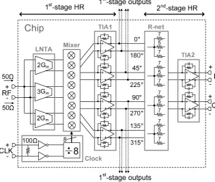
[image:36.595.162.478.257.523.2]Chapter 5 Downconversion Techniques Robust to Out-of-Band Interference
Figure 5.4 Block diagram of the chip implementing the 2-stage polyphase HR and the low-pass blocker filtering
shown in (5.1). The additional more accurate HR follows in the 2nd stage, aiming to
bring residual harmonic images below the noise floor.
5.3.2 Working Principle
We will now show how to accurately approximate 1:√2:1 via 2:3:2 and 5:7:5. A
key point is that the output of the TIA1 stage has 8 IF-outputs with equidistant phases, i.e. 0° to 315° with 45° step, instead of the conventional 4 phases, i.e.
quadrature. This enables iterative HR by adding a 2nd stage. Fig. 5.5 shows the
weighting factor for the 8 outputs of the 1st-stage HR versus time (t) for one
complete period of the LO (T). If we weight and sum three adjacent-phase outputs
of the 1st-stage HR via the 2nd-stage weighting factors 5:7:5, as shown in Fig. 5.6,
Figure 4.1: Software defined radio receiver as reported in [Ru et al.,2009].
4.2
Motivation
The main features of this front-end for beamforming purposes are:
• Low-noise transimpedance amplifier (LNTA), providing 50 Ω input
impedance andV →I conversion
• 8-phase passive mixer
• 2 transimpedance amplifier (TIA) stages • High linearity
4.2. Motivation
4.2.1 Mixer Array
The passive mixer array is driven by an 8-phase local oscillator (LO). The passive mixer simply consists of NMOS switches, which perform the fre-quency translation. In a similar way, i.e. using switches, a Butler BFN can be constructed. Since the LO provides 8 phases, different mixer outputs can be combined to form a Butler beam (in case of multiple antennas). Since the mixer operates in the current domain, the down-converted & phase-shifted signals from multiple antenna-elements are easily summed to form a Butler beam.
4.2.2 TIA Stages
Both Op-Amp stages are configured as a transimpedance amplifier (TIA) via resistive feedback. The transimpedance is largely defined by the feedback resistor. The R-net in between the TIA stages serves as a weighting network for harmonic rejection (HR).
TIA1
In the proposed platform, the first TIA stage is driven by the down-converted LNTA current. When the transimpedance is programmable, the output voltage (1st-stage outputs in Figure 4.1) can be adjusted. In this way a Butler beam can be attenuated by lowering the transimpedance. Thus the first TIA stage can be extended as implementation for the magnitude weights (a) of the beamforming system.
TIA2
4.2.3 Linearity
As becomes clear in the above sections, this architecture is well suited for implementation of the system functions, i.e. the proposed beamforming system. However, the most important feature of this receiver - in the context of beamforming - ishigh linearity.
Especially this property fits the main goal of this work, namely interference nulling. Because of high linearity, this front-end is highly tolerant to strong interferers. In order to prevent clipping to the supply (which is very limited in modern CMOS processes) voltage gain is avoided at RF. Consequently, these blockers can be processed in the current domain from RF to IF and subsequently be suppressed at the first TIA stage where voltage gain occurs. Figure4.2presents the proposed beamforming system, utilizing the features of the above described front-end. In Figure4.2, n represents the number of phase-shifted mixer outputs, which are summed in the summation network to form a Butler beam.
LNTA
LNTA
LNTA
LNTA
Σ
Σ
Σ
Σ n
n
n
n
I
Q
I
Q
I
Q
I
Q
P A1
A2
A3
A4
Butler BFN
(incl. Mixer) a φ Σ
Chapter 5
System Model Evaluation
The previous chapter described a receiver front-end, suitable for implemen-tation of the proposed beamforming system. This chapter evaluates the performance of the beamforming system, subject to constraints imposed by a circuit implementation. In order to model the circuit implementation as shown in Figure4.2, the complex weights of the proposed beamforming sys-tem are quantized. In this chapter, simulations of the syssys-tem model with quantized weights are presented. It will become clear that a circuit imple-mentation imposes constraints to the system performance.
5.1
Circuit Constraints
The proposed platform described in Chapter 4 imposes constraints, which limit the performance. This section addresses these limitations with respect to the (ideal) system design.
5.1.1 Butler Beamforming Network
The proposed front-end provides an 8-phase LO (1
5.1.2 Weight Quantization
The complex weights (C), as determined by the beamforming algorithm (see section 3.3), should be implemented using resistors. A variable resistance can only have a finite number of values. Thus, the complex weights (i.e. resistors) should be quantized. Keeping a circuit implementation in mind, realistic quantization levels are chosen. The beamforming algorithm results magnitude weights (aq) normalized between 0 and 1 and phase weights (ϕq)
normalized between 0◦ and 360◦. Expressing the number of quantization levels in bits (b) results:
aq =
q−1
2b−1 (5.1)
ϕq =
q−0.5
2b 360
◦ (5.2)
where
1≤q≤ 2b
Consider a phasor diagram with a phasor at 0◦ in the first quadrant and a phasor at 90◦ in the fourth quadrant. These vectors overlap. Therefore, ϕ
q
has an 1
2 LSB offset from the I/Q axis.
5.2
Model Simulations
The interference nulled radiation pattern (P) is evaluated for various
quan-tization settings. Figures 5.1 - 5.3 present benchmark curves, to identify the performance of the beamforming algorithm. In each figure, the main beam is steered to u = 0.61, while the position of an interferer is swept from u =−1 (endfire) to u = 0.5, i.e. 30◦. The blue curves represent the magnitude of one of the Butler beams, which is maximal at the position of the interferer. This curve can be considered the nulling performance of the first stage in Figure 4.2. The green curves represent the total nulling per-formance, so including phase shifting and beam summation. The red curves represent the level of the main beam. All curves are relative to 0 dB.
5.2.1 Quantized Butler Phases
Figure 5.1 presents the nulling performance of the beamforming algorithm as a result of constructing the Butler matrix with a limited number of LO
1This value is chosen because, for low resolutions (i.e. strong quantization), a Butler
5.2. Model Simulations
phases. The Butler phases are quantized to 2, 3 & 4 bits. In this way a rotational broadside Butler (i.e. using 4 LO phases) and a rotational
standard Butler (using 8/16 LO phases) can be constructed. The algorithm rotates the Butler matrix such that one of the beams captures the interferer. The magnitude weights (i.e. aq) and the phase weights (i.e. ϕq) are both
quantized to 5 bit.
−1 −0.5 0 0.5
−40 −30 −20 −10 0 10
Interferer position [u−space]
Magnitude [dB]
Interferer Rejection after 1st Stage Interferer Rejection after 2nd Stage Main Beam Ripple
(a) 2-bit Butler matrix
−1 −0.5 0 0.5
−40 −30 −20 −10 0 10
Interferer position [u−space]
Magnitude [dB]
Interferer Rejection after 1st Stage Interferer Rejection after 2nd Stage Main Beam Ripple
(b) 3-bit Butler matrix
−1 −0.5 0 0.5
−40 −30 −20 −10 0 10
Interferer position [u−space]
Magnitude [dB]
Interferer Rejection after 1st Stage Interferer Rejection after 2nd Stage Main Beam Ripple
(c) 4-bit Butler matrix
Figure 5.1: 2-stage nulling performance due to quantized Butler phases.
As mentioned above, the blue curve represents the nulling performance of the first stage. More bits, i.e. more phases, means that a Butler beam can be steered more accurately into the direction of the interferer. Figure 5.1
clearly shows that more Butler phases result more nulls (see the blue dips), which are located at the positions of the Butler beams (see Figure2.4). The green curve shows a large rejection for each scenario, due to the relatively high resolution (5 bit quantization) ofaq&ϕq. The red curve is ideally 0 dB,
but shows some variation due to overall quantization. When the interferer approaches the main beam atu= 0.6, the red curve falls off.
Simulations of the system model result the (minimum) interference rejection figures and the main beam loss for each quantization level. Table5.1presents these figures, which apply to the intervalu= [−1. . .0.1], since fromu= 0.1 the red curve starts to fall off because the interferer approaches the main beam.
Number of quantization bits 2 bit 3 bit 4 bit First stage rejection [dB] -10.07 -11.53 -16.04 Second stage rejection [dB] -34.02 -34.39 -35.10
Main beam loss [dB] -0.80 -0.85 -0.86
5.2.2 Quantized Magnitude Weights
In a similar way, as described in the previous section, the effect of quantizing the magnitude weights (aq) is evaluated. Figure5.2presents the nulling
per-formance of the beamforming algorithm for various quantization levels. The Butler phases are quantized to 3 bit (i.e. 8 phases) and 5 bit quantization is used for the phase weights.
−1 −0.5 0 0.5
−40 −30 −20 −10 0 10
Interferer position [u−space]
Magnitude [dB]
Interferer Rejection after 1st Stage Interferer Rejection after 2nd Stage Main Beam Ripple
(a) 3-bit magnitude weights
−1 −0.5 0 0.5
−40 −30 −20 −10 0 10
Interferer position [u−space]
Magnitude [dB]
Interferer Rejection after 1st Stage Interferer Rejection after 2nd Stage Main Beam Ripple
(b) 4-bit magnitude weights
−1 −0.5 0 0.5
−40 −30 −20 −10 0 10
Interferer position [u−space]
Magnitude [dB]
Interferer Rejection after 1st Stage Interferer Rejection after 2nd Stage Main Beam Ripple
(c) 5-bit magnitude weights
Figure 5.2: 2-stage nulling performance due to quantized magnitude weights.
The blue curves, i.e. first stage rejection, remain relatively constant. How-ever, more bits result smoother curves due to finer quantization steps. The total interference rejection (green curves) improves with approximately 6 dB for each bit that is added. The ripple of the red curve becomes smaller for each bit that is added.
Table5.2presents the (minimum) interference rejection figures and the main beam loss for each quantization level. Again, the presented values in Table
5.2apply to the intervalu= [−1. . .0.1].
Number of quantization bits 3 bit 4 bit 5 bit First stage rejection [dB] -11.32 -11.57 -11.53 Second stage rejection [dB] -22.39 -28.67 -34.39
Main beam loss [dB] -1.10 -0.93 -0.85
Table 5.2: Minimum rejection values due to quantized magnitude weights.
5.2.3 Quantized Phase Weights
Finally, the quantization of the phase weights (ϕq) is examined. Figure
5.3 presents the nulling performance. Both Butler phases and magnitude weights are quantized to 3 bit.
5.2. Model Simulations
−1 −0.5 0 0.5
−40 −30 −20 −10 0 10
Interferer position [u−space]
Magnitude [dB]
Interferer Rejection after 1st Stage Interferer Rejection after 2nd Stage Main Beam Ripple
(a) 1-bit phase weights
−1 −0.5 0 0.5
−40 −30 −20 −10 0 10
Interferer position [u−space]
Magnitude [dB]
Interferer Rejection after 1st Stage Interferer Rejection after 2nd Stage Main Beam Ripple
(b) 2-bit phase weights
−1 −0.5 0 0.5
−40 −30 −20 −10 0 10
Interferer position [u−space]
Magnitude [dB]
Interferer Rejection after 1st Stage Interferer Rejection after 2nd Stage Main Beam Ripple
(c) 3-bit phase weights
Figure 5.3: 2-stage nulling performance due to quantized phase weights.
first stage, the (quantization) requirements for the phase weights (i.e. the vector modulator) are heavily relaxed. Therefore, using more bits, does not result better nulling performance. The ripple of the main beam is smoothed, in case more bits are used.
Table5.3presents the (minimum) interference rejection figures and the main beam loss for each quantization level. Once again, the values in Table 5.3
apply to the intervalu= [−1. . .0.1].
Number of quantization bits 1 bit 2 bit 3 bit First stage rejection [dB] -11.32 -11.32 -11.32 Second stage rejection [dB] -9.14 -14.58 -22.39
Main beam loss [dB] -1.63 -1.36 -1.10
Chapter 6
Circuit Level Design
In this chapter, circuits are proposed to implement the beamforming system. As addressed in Chapter 5, a circuit implementation imposes constraints, in terms of performance, compared to the ideal system model. These con-straints (i.e. quantization) serve as specification for the circuit implementa-tion. Thesecircuit specifications are:
• Maximal 8 LO phases for synthesizing the Butler BFN. • 3-bit linear transimpedance setting in the first TIA stage. • 5-bit uniform phase setting in the second TIA stage.
6.1
Beamforming Front-End
In Figure 6.1, a four-element linear array feeds the front-end, which ac-commodates four signal paths. Each path consists of a low-noise transcon-ductance amplifier (LNTA), providing 50 Ω input impedance and V → I conversion. Subsequently, a passive mixer array, operating in the current domain, performs frequency translation. Each transconductance block con-sists of four small LNTAs, driving the mixer blocks. At IF, a summation network constructs four Butler beams. The passive mixer array together with the summation network, implement the Butler BFN.
The first TIA stage, with programmable transimpedance, implements the magnitude weights (aq), weighting the Butler beams and performingI →V
64 A1 A2 A3 A4 A11 A12 A13 A14 A21 A22 A23 A24 A31 A32 A33 A34 A41 A42 A43 A44 Σ Σ Σ Σ 4x 4x 4x 4x I Q I Q I Q I Q 4x P Butler BFN (incl. Mixer) Vector Modulator
Figure 6.1: Front-end based on [Ru et al.,2009] suitable for beamforming.
Figure 6.1 shows the proposed beamforming system using 4 LO phases, such that a broadside Butler BFN can be implemented. In a similar way an 8-phase system can be constructed, using 8 signal paths. However, on behalf of circuit complexity and to save simulation time, a 4-phase system is actually implemented and simulated, in order to verify the functional operation. Therefore, the following sections apply to the ’4-phase version’ of the proposed beamforming system.
6.2
Mixer Block
The passive mixer array in Figure 6.1 consists of 16 mixer blocks. Figure
6.3. Butler BFN
In case these mixer blocks would not be driven by separate LNTAs, an undefined current distribution between the virtual grounds of the first TIA stage would occur, leading to a pre-weighting of the Butler beams, which is unwanted. In addition, noise & offset problems can arise.
CLK0
CLK90
CLK180
CLK270
OUT_0
OUT_90
OUT_180
OUT_270 IN
Figure 6.2: Passive down-conversion mixer.
Note that the phases for the Butler BFN are generated in these mixer blocks.
6.3
Butler BFN
A Butler beamformer is implemented as shown in Figure6.3. Four of these configurations, implement the whole Butler BFN.
Σ
A11
A21
A31
A41
1R
Figure 6.3: Implementation of a Butler beamformer.
6.4
TIA Stage
As already suggested in section 4.2.2and described in section 6.1, the first TIA stage in Figure6.1implements the magnitude weights (aq) of the
beam-forming system. To map these magnitude weights to this resistor - Op-Amp arrangement, the feedback resistance should be made programmable. The feedback resistance can either be a series network or a parallel network of resistors. To obtain a linear increase in transimpedance, a series network is a natural choice.
6.4.1 Proposed Circuit Implementation
Figure6.4 presents the circuit implementation of magnitude weights in the first TIA stage.
C
FBM0
P0
a0
a0
R R
M1 R
M2 M7
a1 a2
a7
IIN
VOUT
Figure 6.4: TIA with 3-bits programmable transimpedance.
According to the circuit specifications, the transimpedance should be lin-early adjustable and 3-bits programmable. A resistor string of 23−1 resistors (R) is used as feedback network. Each node between two successive resistors can be switched to virtual ground at the inverting input of the Op-Amp. NMOS switches M1-M7 are used to set the transimpedance. M0 and (com-plementary driven) P0, are used for setting the lowermost magnitude weight, i.e. 0, simply by dumping the input current to ground. Only one switch at a time can be on, since the input vector aq is thermometer coded. The
6.4. TIA Stage
6.4.2 Transimpedance
RF input power typically ranges from -40 to -30 dBm. However, accord-ing to [Ru et al., 2009], inband interference can be as strong as 30 to -20 dBm. Consider an in-band interferer of --20 dBm, i.e. 10µW input power.
Since the LNTA stage performs a transconductance of 20 mS, i.e. 50 Ω tran-simpedance, it can be derived what the maximum transimpedance for the first TIA should be, in order to prevent clipping to the supply.
According toP = VR2, 10µW input power results an rms voltage of
approxi-mately 22.36 mV when dissipated in a resistor of 50 Ω. Assuming a sinusoidal input signal, this corresponds to an amplitude of 31.62 mV. Consequently 20× voltage gain (i.e. VT OP = 632 mV) can clip an in-band interferer of
-20 dBm to a 1.2 V supply, when biased at 1
2VDD (i.e. VCM = 600 mV).
6.4.3 MOST Switches
When an NMOS transistor operates in triode region, its drain current is [Razavi,2001, p. 17]:
ID =µnCox
W L
(VGS−VT H)VDS −
1 2VDS2
(6.1)
To let a MOS transistor operate as a switch, the device must be in deep triode region. That isVDS<<2(VGS−VT H). Hence the quadratic term in
(6.1) can be neglected, so (6.1) becomes:
ID ≈µnCox
W
L [(VGS−VT H)VDS] (6.2) The drain current has become a linear function of the drain-source voltage, hence the transistor operates as a linear resistor. WritingRon= VID
DS results:
Ron=
1
µnCoxWL(VGS−VT H)
(6.3)
An ideal switch has an on-resistance (Ron) of 0 Ω. To operate as a switch,
a MOS transistor should have an Ron as small as possible. According to
(6.3), a low on-resistance can be obtained by increasing the width of the transistor (W) or increasing the gate-source voltage (VGS). In practice,
both parameters are used to lower Ron.
Furthermore it is desired to keep Ron constant. Note the position of the
CFB
M7 R
VOUT
a7
IIN
Figure 6.5: Voltage swing modulating Ron.
The input current (IIN) causes voltage swing at the source of M1, due to the
resistor. Consequently the gate-source voltage of M1 is modulated according toIIN. Thereby changingRonand hence introducing nonlinearity. In Figure
6.4all NMOSTs have their source tied at the inverting input of the Op-Amp, i.e. virtual ground. In this way the gate-source voltage is relative constant and thusRon remains relatively constant.
6.4.4 Charge Pump
In order to obtain a relatively lowRon compared to the total feedback
resis-tance, a high gate-source voltage is desired. Since the common-mode level is halfVDD, i.e. VCM = 600 mV, the gate-source voltage is limited to:
VGS=VDD−VCM = 1.2−0.6 = 600 mV
The used NMOS transistors have a threshold voltage (VT H) of 415 mV.
Consequently, the maximum overdrive (VGS−VT H) is 185 mV, which is too
low for Ron. Therefore, a voltage higher than VDD is necessary in order
to obtain a sufficiently lowRon. A common solution is to employ a charge
pump, which can generate a voltage higher than the supply from which it is operating. A useful introduction is given by [Pylarinos].
Figure6.6 presents a charge pump. Note that this thesis does not focus on charge-pump design. However, an example is presented to illustrate that such a circuit can be used in order to obtain voltages well above the supply. WhenVCLK goes low (i.e. 0 V), point A is grounded such that C1 is charged
6.5. Vector Modulator
____ VCLK
C1
VOUT
VCLK
VDD
VDD
VDD
C2
C3
CLOAD
M1
M2
M3 M4 A
B
C
Figure 6.6: Charge pump from [Baker,2010,§18.4.1].
sense a voltage of:
VDD+VC1 =VDD+ (VDD−VT H) = 2VDD−VT H
This causes M2 & M3 to turn on, so that points B & C are pulled toVDD.
When VCLK returns back to zero (i.e. VCLK =⇒ VDD), the sources of M2
& M3 swing up to 2VDD, such thatCLOAD is charged to 2VDD−VT H.
The output voltage reaches 1.77 V with a 1.4 mV ripple using minimum sized transistors and a load capacitor of 150 fF. Due to non-idealities, the simulated output voltage is 215 mV lower than the theoretical value.
6.4.5 Bandwidth
The bandwidth of the first TIA stage is limited to 20 MHz. This should be sufficient in order to accommodate most mobile communication standards [Ru et al.,2009,§5.4.4]. The feedback capacitor (CF B) limits the bandwidth
for a fixed resistance according to:
B−3 dB= 1 2πRCF B
(6.4)
6.5
Vector Modulator
6.5.1 Vector Modulation
Figure6.7presents a phasor diagram, in order to illustrate the phase shifting function by means ofvector modulation. A phasor (or phase vector) can be
defined as the sum of a horizontal component (i.e. vector I) and a vertical component (vector Q). In Figure6.7, the lengths of these I & Q vectors are linearly modulated via uniform steps (denoted by ∆L). The I/Q vectors are complementary in length, so when vector I increases by ∆L, vector Q decreases by ∆L and vice versa.
Magnitude Error
I Q
ΔL
0° 180°
90°
270°
Figure 6.7: Phasor Diagram with linear modulated I & Q vectors.
As becomes clear from Figure 6.7, using uniform steps (i.e. weights) for the I & Q vectors, results into a magnitude error (i.e. a deviation from the unit circle). This error is undesired, since the contributions of each signal path in the front-end of Figure 6.1 need to be properly summed, in order to render the correct radiation pattern. Figure 6.8presents a phasor diagram illustrating aproper vector modulator function, which is described
by Euler’s formula:
ejϕ = cos(ϕ) +jsin(ϕ) (6.5)
0° 22.5° 45°67.5°90°
I Q
6.5. Vector Modulator
In Figure6.8, the length of the Q vector is modulated according to the sine function. Likewise, the length of the I vector is modulated according to the cosine function (not illustrated). So, the horizontal & vertical components of the phasors are modulated by sinusoidal steps. In other words:
A uniform phase step requires non-uniform weights for the I & Q vectors.
This property of a vector modulator was already presented in [Soer et al.,
2011], where the weights, modulating the lengths of the I/Q vectors, approx-imate the sine/cosine curves via a switched-capacitor charge distribution network. In this work the idea, as introduced in section 1.4, is to imple-ment the weights via resistors. According to the circuit specifications, the vector modulator should have a 5-bit uniform phase setting (for comparison purposes).
6.5.2 Synthesis of the Weights
To obtain the result of (6.5), the I & Q vectors have to be weighted according to the cosine & sine functions respectively. As shown in Figure 6.1, the vector modulator senses (differential) in-phase & quadrature components of the output voltage of the first TIA stage, i.e. VI &VQ. Since currents need
to be summed at the virtual ground of the second TIA stage,VI &VQ need
to be weighted by resistors, which performV →I conversion, writing:
I = VI RI
+ VQ
RQ
(6.6)
In order to describeRI &RQ, a resistorR0 is defined:
RI =
R0
cos(ϕ) (6.7a)
RQ =
R0
sin(ϕ) (6.7b)
Such that (6.6) becomes:
I = VI
R0cos(ϕ) + VQ
R0 sin(ϕ) (6.8)
Since V → I conversion is performed, i.e. conductance, the inverse of R0 can be considered the length of the phasor:
1 R0 =
s
1
RI
2
+
1
RQ
2
Using (6.7) and a value of 1207 Ω1 for R0, gives the values for R
I & RQ,
which are listed in Table 6.1:
R0 = 1207 Ω RI[Ω] RQ[Ω]
5.625◦ 1213 12315 16.875◦ 1261 4158 28.125◦ 1369 2561 39.375◦ 1562 1903 50.625◦ 1903 1562 61.875◦ 2561 1369 73.125◦ 4158 1261 84.375◦ 12315 1213
Table 6.1: Resistor values for RI &RQ weighting the I/Q signals.
6.5.3 Implementation of the Weights
In order to implement the I & Q resistors, their values as presented by Table
6.1have to be round off. It is assumed that the maximum difference between the smallest and the largest resistance is 6 bit (i.e. 64×). A numerical
analysis (using Matlab) is performed in order to find a resistor valueR, of which integer multiples approximate the resistor values listed in Table 6.1
with minimal deviation. The analysis results that multiples of R = 116 Ω yields, on average, the smallest deviation.
Table6.2presents the (rounded) values for RI2, using a resistance of 116 Ω.
R = 116 Ω n nR[Ω] RI[Ω] Abs. Error [Ω] Rel. Error [%]
5.625◦ 10 1160 1213 53 4.37
16.875◦ 11 1276 1261 15 1.19
28.125◦ 12 1392 1369 23 1.68
39.375◦ 13 1508 1562 54 3.46
50.625◦ 16 1856 1903 47 2.47
61.875◦ 22 2552 2561 9 0.35
73.125◦ 36 4176 4158 18 0.43
84.375◦ 100 11600 12315 715 5.81
Table 6.2: Rounded resistor values ofRI.
1
The value of 1207 Ω would appear strange. When following a slightly different design procedure, as presented in this section, this value was numerically convenient.
2
6.5. Vector Modulator
6.5.4 Proposed Vector Modulator Implementation
The first TIA stage in Figure6.1, provides voltage outputs. Using resistors to performV →I conversion, the quadrature vectors (i.e. I/Q currents) are weighted and subsequently summed to obtain the desired phase shift. Figure 6.9presents the circuit implementation of the vector modulator.
VI
x7
x1
x0
y0 y1 y7
VQ
RFB
10R R 64R
10R R 64R
VOUT
Figure 6.9: Circuit implementation of the vector modulator.
The entire resistor ladder is illustrated in Figure6.10, synthesizing the values forRI. Note that the total resistance accumulates to 100·116 = 11600 Ω.
VI
10R R R R 3R 6R 14R 64R
Chapter 7
Simulation Results
The circuits, as proposed in Chapter 6, are simulated using SpectreRF. These circuits are not optimized to meet a specific design parameter, such as noise, power consumption, etc. The circuits are simulated in order to ver-ify the functional operation of the proposed implementation. This chapter first describes the simulation setup. Subsequent sections present