DESIGN AND OPTIMIZATION OF
PULSED MODE SILICON BASED DDR
IMPATT DIODE OPERATING AT 0.3 THz
ARITRA ACHARYYA
Institute of Radio Physics and Electronics, University of Calcutta, 92 APC Road, Kolkata-700009, India.
J. P. BANERJEE
Institute of Radio Physics and Electronics, University of Calcutta, 92 APC Road, Kolkata-700009, India.
Abstract:
Properties and performance of DDR p+pnn+ Silicon IMPATT diode at 0.3 THz frequency has been investigated for optimum bias current density through modeling and simulation technique. A double iterative computer method based on drift-diffusion model has been used to study the DC and small signal admittance properties of the device. The bias current density is optimized with respect to maximum conversion efficiency and device negative resistance at 0.3 THz. The simulation studies show that this device is a potential source for generating high RF power at 0.3 THz. The DC-to-RF conversion efficiency of the device is found to be 6.53 % at 0.3 THz at the optimum bias current density of 18×108 Amp/m2. The design results presented in this paper will be useful to realize experimentally Si IMPATTs for Terahertz frequencies.
Keywords: Admittance characteristics; Double drift region; IMPATT; Optimum bias current density.
1. Introduction
IMPact Avalanche Transit Time (IMPATT) diodes have emerged as very important solid state sources capable of generating high frequency RF power at microwave [2-3], millimeter wave and sub-millimeter wave frequency bands. In view of the simple arrangement, low cost, tuning capability, frequency coverage, output power and reliability, Impatt devices have found a variety of applications as solid state transmitters in tracking Radars, Missile seekers, Radiometers and Millimeter wave communication systems. The Terahertz domain is enriched with the emerging possibilities in the fields of Remote sensing, Imaging, Spectroscopy and Communication with unique application for detecting hidden biological weapons and explosives. The development of reliable solid state semiconductor devices operating in the Terahertz frequency region has therefore attracted the attention of researchers worldwide [4]. During last decade, significant efforts were made to realize solid-state sources that may generate THz power. Among all the available solid state sources, IMPATT diodes have already emerged as the most efficient source for its ability to deliver high RF power even at 300 GHz or more. It is well known that the RF power depends on various factors like critical field for avalanche breakdown, saturation drift velocity for charge carriers, etc which varies for different semiconductor materials and play vital role in limiting the output power of an IMPATT diode at a particular operating frequency. Silicon and Gallium Arsenide Impatt diodes have been established as reliable sources. However due to rapid technological advancement and better high frequency properties, Silicon emerged as the most powerful and popular base material for IMPATT devices.
To the best of the authors’ knowledge, no experimental results on fabrication of Si based IMPATT diodes at
0.3 THz are available in the literature. However some studies on Si IMPATTs have been reported lately at this frequency. In the sub-millimeter/Terahertz region high power IMPATT oscillators are extremely useful solid state sources. To satisfy the quest of increasing demand for high power terahertz sources in various strategic, civilian and defense applications, the authors have designed Silicon based DDR IMPATT diode at terahertz domain for their optimum performance. A flat profile p+pnn+ device structure has been taken for operation at
The rest of the paper is organized as follows. Section II describes the simulation methodology of IMPATT devices. In Section III entire design methodology is described along with the necessary results in form of graphs and tables. Finally the paper concludes in Section IV.
2. Simulation Methodologies
2.1 Design of Doping Profile
The frequency of operation of an IMPATT diode essentially depends on the transit time of charge carriers to cross the depletion layer of the diode. A double drift p+pnn+ structure of Si IMPATT have been designed by using computer simulation technique for operation at 0.3 THz frequency by using the transit time formula of Sze and Ryder which is Wn,p = 0.37 vsn,sp / f; where Wn,p, vsn,spand f are the total depletion layer width (n or p -side), saturation velocity of electrons/holes and operating frequency respectively. Here n+ and p+-layers are highly doped substrates and n and p are epilayer.
2.2 Material and Design Parameters
The material parameters of Silicon (at 500 K) are enlisted in TABLE I and design parameters of the same are shown in TABLE II.
TABLEI
MATERIAL PARAMETERS OF SILICON AT 500K
PARAMETER VALUE
*
Ionization coefficient of electrons at low fields, An (×108 m-1) 0.620
*
Ionization coefficient of electrons at low fields, bn (×108 V/m) 1.340
*
Ionization coefficient of holes at low fields, Ap (×108 m-1) 2.000
*
Ionization coefficient of holes at low fields, bp (×108 V/m) 2.190
*
Ionization coefficient of electrons at high fields, Ahn(×108 m-1) 0.500
*
Ionization coefficient of electrons at high fields, bhn (×108 V/m) 1.250
*
Ionization coefficient of holes at high fields, Ahp (×108 m-1) 0.560
*
Ionization coefficient of holes at high fields, bhp(×108 V/m) 1.540
Saturation drift velocity of electrons, vsn (×105 m/s) 0.643
Saturation drift velocity of holes, vsp (×105 m/s) 0.634
Mobility of electrons, μn (×10-1 m2V/s) 0.500
Mobility of holes, μp(×10-1 m2V/s) 0.180
Permittivity, ε (×10-9 F/m
) 0.104 *α
n and αp are rapidly increasing function of electric field. Experimentally obtained values of αn and αp can be
approximately fitted with the empirical formula, αn,p = An,p exp((-bn,p/E)m). For high fields Ahn,hp and bhn,hp are
used in place of An,p and bn,p (Table IV). Value of m depends on the base material. For silicon, m = 1 [9].
TABLEII DESIGN PARAMETERS
Operating Frequency, (THz) 0.3
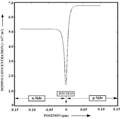
n-epitaxial layer doping concentration, (×1023 m-3) 5.20
p-epitaxial layer doping concentration, (×1023 m-3
) 6.80
n+-substrate layer doping concentration, (×1026 m-3) 1.00
Width of the n-layer, (μm) 0.140
Width of the p-layer, (μm) 0.110
2.3 Computer Simulation Techniques
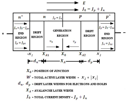
In the computer simulation of DC and small-signal behavior of the Si DDR IMPATT diode, the following assumptions are made, viz., (i) one dimensional model of the p-n junction is treated (Fig. 1); (ii) the electron and hole velocities are taken to be saturated and independent of the electric field throughout the space charge layer.
Fig. 1 The Active Layers of a Reverse Biased p-n junction.
The simulation method starts with DC analysis described in details elsewhere [5, 7, 8]. In this method the computation starts from the field maximum near the metallurgical junction. The distribution of DC electric field and carrier currents in the depletion layer is obtained by the double-iterative computer method, which involves iteration over the magnitude of field maximum (Em) and its location in the depletion layer. A computer algorithm has been developed for simultaneous numerical solution of Poisson’s equation, carrier continuity equations and the space charge equation taking into account the effect of mobile space charge and carrier diffusion in order to obtain the electric field profiles and carrier current profiles. The boundary conditions for the electric field at the depletion layer edges are given by,
x 0 and E
x
0E 1 2 (1)
Where, -x1 and x2 define the p+ and n+edges of the depletion layer (origin at the junction). The boundary conditions for normalized current density P(x) = (Jp – Jn)/J0 (where, Jp = hole current density, Jn = electron current density) at the edges are given by,
n 2 p 1 M 2 1 x P and 1 M 2 xP (2)
The necessary device equations have been simultaneously solved [5] satisfying the appropriate boundary conditions mentioned in (1) and (2). The field dependence of electron and hole ionization rates (αn and αp) and saturated drift velocities of electron (vsn) and holes (vsp) at 500 K are made use of in the computation for the profiles of electric field and carrier currents. The conversion efficiency is calculated from the approximate formula [6],
B D V V m 2 % (3)Where, VD = Voltage drop across the drift region, VB = Breakdown voltage and m = ½.
Avalanche breakdown occurs in the junction when the electric field is large enough such that the charge multiplication factors (Mn, Mp) become infinite. Again, the breakdown voltage is calculated by integrating the spatial field profile over the total depletion layer width, i.e.,
2 1 x xB Exdx
V (4)
2 1 2 1 x x X x xR Rdx and Z Xdx
Z (5)
The negative conductance (G), Susceptance (B) and the quality factor (Q) of the device can be calculated using the following relations:
2
X 2 R X 2 X 2 R
R/Z Z and B Z /Z Z
Z
G
(6)
at peak frequencypeak B/G
Q
(7)
It may be noted that both –G and B are normalized to the area of the diode. The avalanche frequency (fa) is the frequency at which the imaginary part (B) of the admittance changes its nature from inductive to capacitive. Again it is the minimum frequency at which the real part (G) of admittance becomes negative and oscillation starts to build up in the circuit.
At a resonant frequency of oscillation, the maximum RF power output (PRF) from the device can be obtained from the following expression,
A . G . V . 2 1
PRF RF2 p (8)
Where, VRF is the amplitude of the RF swing (VRF=VB/2, assuming 50% modulation of the breakdown voltage
VB), Gp is the diode negative conductance at the operating frequency and A is the area of the diode (10-8 m2). The accuracy of the our method of DC and Small-Signal simulation of IMPATT devices is increased by incorporating realistic doping profiles, considering recently reported values of material parameter at 500 K (TABLE II) and including the effect of mobile space charge.
3. Results and Discussions
The various design parameters used to study the DC and high frequency properties of Si DDR IMPATT diode at 0.3 THz are given in Table I & Table II respectively. Simulated DC parameters of the diode for different bias current densities are tabulated in Table III.
In Fig. 2 the doping profile of designed diode is shown. Fig. 3 shows the electric field profiles of the diode at different bias current densities.
Fig. 2 Doping profile of the diode.
Fig. 3 Electric field profiles of the diode at different bias current densities (mentioned in Table III).
TABLEIII SIMULATED DC PARAMETERS
PARAMETERS SET-I SET-II SET-III SET-IV SET-V
BIAS CURRENT DENSITY,
J0 (×108 Amp/m2)
16 18 20 22 24
PEAK ELECTRIC FIELD,
Em (×107 Volt/m)
8.9999 8.9499 8.8999 8.8249 8.7749
BREAKDOWN VOLTAGE,
VB (Volt)
11.64 11.75 11.87 11.90 12.01
EFFICIENCY,
η (%)
6.4445 6.5279 6.3960 6.2800 6.2212
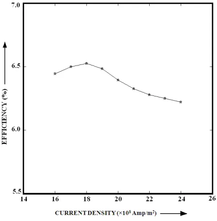
It is observed from Table III and Fig. 3 that the peak electric field (Em) at the p-n junction decreases with the increase in current density. The E(x) profiles at high bias current levels are found to be punch through type. The avalanche zone width is obtained from the region of the depletion layer near the junction where the current grows through avalanche multiplication to 95% of its DC value (J0). Table III reveals that with the increase of current density, the field maximum decreases gradually, and also due to the increasing space charge effect, efficiency degrades from 6.4445 % to 6.2212 %. The conversion efficiency (η) increases very slowly at lower range of current density and attains a maximum value of η = 6.5279 % at bias current density of 18×108
Amp/m2
, and then again starts to decrease with increasing bias current densities. Thus the optimum bias current density for the device operation 0.3 THz frequency is obtained as 18×108 Amp/m2. As we further increase the bias current density, the efficiency actually falls owing to the mobile space charge effect. The optimum bias current density has been found to be 18×108 Amp/m2 where the DC-to-RF conversion efficiency is of maximum value 6.5279 % as is evident from Fig. 4. The breakdown voltage in this case is 11.64 V at a current density of
Fig. 4 Efficiency as a function of bias current density.
The small signal results of the device at different bias current densities are shown in Table IV. The admittance plot (G-B) of Flat profile Si DDR IMPATT diode is shown in Fig. 5. As the bias current density increases the operating frequency also increases. At the optimum bias current density (18×108 Amp/m2) the operating frequency fortunately exactly matches with the design frequency (0.3 THz). Peak negative conductance of the diode continuously increases with bias current density, but the Q-factor decreases with it. The Q-factor determines the growth rate and stability of oscillation. Less Q-factor means better device performance.
TABLEIV
SIMULATED SMALL-SIGNAL PARAMETERS
PARAMETERS SET-I SET-II SET-III SET-IV SET-V PEAK OPERATING
FREQUENCY,
fp (THz)
0.295 0.300 0.304 0.310 0.317
PEAK CONDUCTANCE,
GP (×107 S/m2)
-23.9039 -25.1231 -26.2673 -27.1052 -28.1645
PEAK SUSCEPTANCE,
BP (×107 S/m2)
75.5727 76.7113 77.9376 75.2656 76.5322
QUALITY FACTOR,
Q = (-BP/GP)
3.16 3.05 2.96 2.78 2.72
NEGATIVE RESISTANCE,
ZR (×10-8 Ohm.m2)
-0.03821 -0.03856 -0.03883 -0.04245 -0.04290
PULSED POWER OUTPUT,
P (Watt)
40.4841 43.3570 46.2623 47.9796 50.7806
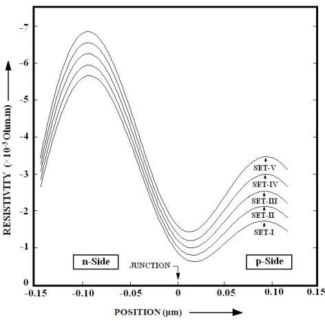
Negative resistivity profiles of the device for different current densities are shown in Fig. 6. Clearly from Fig. 6 and Table IV it can be concluded that as the bias current density increases the negative resistance of the diode improves. As the RF power output is directly proportional to the square of breakdown voltage and magnitude of negative conductance (equation (8)), and as both of then improves with increasing bias current density (Table III and Table IV), so pulsed power output also improves. At optimum bias current density (18×108 Amp/m2) we get sufficient output pulsed power (43.3670 Watt) for pulsed mode of operation (A = 10-8
m2).
Fig. 5 Small-Signal Conductance-Susceptance plot.
Fig. 6 Negative Resistivity profile.
4. Conclusions
based IMPATTs will be highly suitable for operation in Terahertz frequency region in near future. Further the design results presented in this paper will be useful to realize experimentally Si IMPATTs for Terahertz frequencies.
Acknowledgments
The authors wish to thank Miss Moumita Mukherjee [Research Associate, Centre of Millimeter wave Semiconductor Devices and Systems, Institute of Radio Physics And Electronics, University College of Science And Technology (University of Calcutta)] for her valuable suggestions.
References
[1] H. K. Gummel and J. L. Blue, “A Small-Signal Theory of Avalanche Noise in IMPATT Diodes”, IEEE Trans. on Electron Devices, vol. ED-14, no. 9, pp. 569-580 (1967).
[2] T. A. Midford and R. L. Bernick, “Millimeter Wave CW IMPATT diodes and Oscillators”, IEEE Trans. Microwave Theory Tech., vol. 26, pp. 483-492, (1979).
[3] M. Mukherjee and J. P. Banerjee, “DDR Pulsed IMPATT Source at MM-Wave window Frequency: High Power Operation Mode”, Int. J. of Advanced Science and Technology, vol. 16, pp. 11-20, (2010).
[4] M. Mukherjee, S. Banerjee and J. P. Banerjee, “Dynamic Characteristics of III-V and IV-IV Semiconductor Based Transit Time Devices in the Terahertz Regime: A Comparative Analysis”, Terahertz Science and Technology, vol. 3, pp. 97-109, (2010).
[5] S. K. Roy, J.P. Banerjee and S. P. Pati, “A Computer analysis of the distribution of high frequency negative resistance in the depletion layer of IMPATT Diodes”, Proc. 4th Conf. on Num. Anal. of Semiconductor Devices (NASECODE IV) (Dublin) (Dublin: Boole), pp. 494-500, 1985.
[6] H. Eisele and G. I. Haddad, “Microwave Semiconductor Device Physics” (Ed. S. M. Sze), p. 343, Wiley, New York, 1997.
[7] Aritra Acharyya, Moumita Mukherjee, J.P. Banerjee, “Effect of Carrier Diffusion on the Parasitic Positive Series Resistance of Millimeter Wave DDR Si-IMPATT Diodes [W-Band]”, International Conference on Communication, Computers and Devices, Kharagpur, INDIA, December 10-12, 2010.
[8] Aritra Acharyya, Moumita Mukherjee, J. P. Banerjee, “Noise Performance of Millimeter-wave Silicon Based Mixed Tunneling Avalanche Transit Time (MITATT) Diode”, International Journal of Electrical and Electronics Engineering, WASET, vol. 4, no. 8, pp. 589-596, year-2010.
[9] G. Gibbons, “Avalanche-diode microwave oscillators”, Oxford University Press, 1973.
Aritra Acharyyareceived his M.Tech. Degree from Institute of Radio Physics and Electronics, University of Calcutta, Kolkata, W.B., India. Earlier he obtained his B.E. Degree from Bengal Engineering and Science University, Shibpur, Howrah, W.B., India. He worked on Studies on Series Resistance of Millimeter Wave Si-IMPATT Diodes for his Master’s thesis, with emphasis on various physical effects like effect of carrier diffusion and tunneling current on series resistance of IMPATT devices. His research interest is Microwave and Millimeter-wave Semiconductor Devices more specifically IMPATT Devices. He is the first author of 15 research papers in different national and international journals and conference proceedings and more than 8 papers are under review in different international and national journals.
Professor (Dr.) J.P. Banerjeeobtained B.Sc. (Hons.) and M.Sc. in Physics and Ph.D. in Radio Physics
and Electronics from University of Calcutta. He worked as a senior scientist of a Department of Electronics project in Institute of Radio Physics and electronics, C.U. during 1986-1989.
He joined the Department of Electronic Science, C.U. in 1989 as a reader. He has been working as a professor in the Institute of Radio Physics and Electronics, C.U. since 1998.
He is the recipient of Indian National Science Academy Award of a visiting fellowship and Griffith Memorial Prize in Science of the Calcutta University in 1986. He is the principle co-author of more than 130 research papers in International Journals in the fields of Semiconductor Science and Technology, Microwave and Millimeter wave avalanche transit time devices and avalanche Photo Detectors. He has successfully carried out a number of research projects of Government of India on IMPATT diodes. A collaborative research work in the field of computer analysis, fabrication and characterization of V-Band silicon double low high low IMPATTs was successfully carried out by Dr. Banerjee for the first time with Dr. J.F. Luy the eminent German Scientist of Daimler Benz research centre. He is a Fellow of Institute of Electronics and Communication Engineers (IETE), a life member of society of EMI and EMC and Semiconductor Society, India. He is an expert committee member of All India Council of Technical Education and served as a referee