SINGLE CDBA BASED CURRENT
MODE FIRST ORDER
MULTIFUNCTION FILTER
RISHI PAL
Department of Physics, Mizoram University,Aizawl, India. [email protected]
RAMESH CHANDRA TIWARI
Department of Physics, Mizoram University, Aizawl, India [email protected]
RAJESHWARI PANDEY
Dept.of Electronics and Communication Engineering, Delhi Technological University, Delhi, India. [email protected]
NEETA PANDEY
Dept.of Electronics and Communication Engineering, Delhi Technological University, Delhi, India. [email protected]
Abstract:
In this paper, a current-mode (CM) multifunction first order filter configuration using single current differenc buffered amplifier (CDBA) is proposed which can be used to synthesize lowpass (LP), highpass (HP) filter functions simultaneously. The proposed topology can be modified to include an allpass (AP) filter function with the help of programmable switches. Workability of the proposed topolgy is demonstrated through PSPICE simulations using current feedback operational amplifier (CFOA) based realization of CDBA.
Keywords: CDBA; Multifunction filter; current mode processing. 1. Introduction
Electronic filter is an essential building block of continuous time signal processing and finds extensive application in communication and instrumentation systems. These filters can be designed using classical voltage-mode (VM) op-amps, however these circuits have a limitation on their maximum frequency operation due to lower slew rate and constant gain-bandwidth product of the op-amps. During the last few decades, the CM processing has emerged a viable alternative over VM processing due to its inherent advantages like wider bandwidth, greater linearity, and larger dynamic range. Advancements in current mode processing have led to the emergence of new analog building blocks as detailed in [1] and refrences cited there in. The CDBA among those is of relatively recent origin [2] which exploits all advantages offered by current mode processing. Additionally due to its low input impedance terminals, CDBA is free from parasitic capacitances and hence is appropriate for high frequency operation. It provides further flexibility to the designers, enabling a variety of circuit designs, as it can operate in both current and voltage mode. An extensive literature review suggests that though the CDBA has extensively been used for design of biqadratic [3-8] and higher order filters [9, 10] but only a limited number of first order filters [11-14]have been reported and they provide only all pass filtering function.
In this paper, a CM first order multifunction filter configuration using single CDBA is presented which realizes the LP and HP filter functions simultaneously. The proposed topology is further modified to include AP filter function with the help of programmable switches. The passive sensitivities are very low for the proposed configuration. The SPICE simulation results are included to verify the functionality of proposed filter configuration.
2. Circuit Description
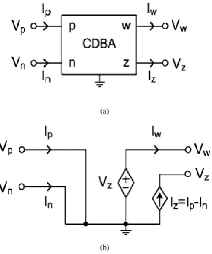
The equivalent circuit of CDBA is shown in Fig. 1(b).The proposed filter topology is shown in Fig. 2. Routine analysis of the circuit of Fig. 2 results in the following transfer function functions
)
1
(
1
eq
sCR
eq
sCR
in
I
I
(2))
1
(
2
2
eq
sCR
R
eq
R
in
I
I
(3)where Req =R1 R2
(a)
(b)
Fig.2. Proposed CM first order multifunction filter.
The current transfer function of (2) represents an HP response whereas the one expressed by (3) is an LP response. The cutoff frequency (ω0) for both the responses is given as
)
(
1
0
eq
CR
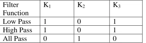
(4)It is a well known fact that using a first order structure, only LP, HP and AP responses can be obtained. The proposed filter topology of Fig. 2, which provides LP and HP responses only, can be extended to provide the AP response as well with the help of programmable switches as shown in Fig.3. The LP, HP and AP responses can be obtained with the switch settings given in Table 1. A switch can be implemented using MOS transistor with gate voltage used for controlling the switch closure.
Table 1. Switch settings for various filter function.
Filter
Function
K
1K
2K
3Low Pass
1
0
1
High Pass
1
0
1
All Pass
0
1
0
With switch settings K1 = K3 = 1, K2 = 0, the transfer function for I1 and I2 are given by equations (2) and (3) respectively whereas with K1 = K3 =0 and K2 = 1 the transfer function at I2 is given by
)
1
/
1
(
)
1
/
1
(
2
CR
s
CR
s
in
I
I
(5)which represents an AP function having phase response as
))
1
arctan(
2
180
(
)
(
CR
(6)The sensitivities of ω0 with respect to each passive component are low and obtained as
1
0
0
2
0
1
Fig.3. Modified CM first order multifunction filter.
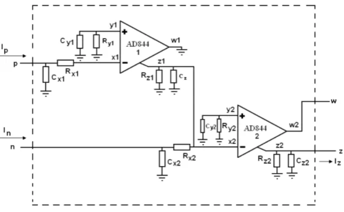
3. Realizing a CDBA and associated non ideality analysis
For the proposed configuration, the CDBA was realized using AD844 CFOA IC as shown in Fig. 4 [2]. Ideally the input resistance at the x terminal is zero and is infinite at the z terminal. From Fig. 3 various currents can be calculated as
p
z
I
I
1 (8)1
2 n z
x
I
I
I
(9)
2
2 x
z
I
I
(10)Therefore Iz, the current from z terminal can be calculated as
)
-(
12 p n
z
z
I
I
I
I
(11)And the output voltage Vw is given as
z
w
V
V
(12)Fig. 5. CDBA realization with nonideal model of AD844
Using this nonideal model for CFOA the CDBA structure of Fig.4 modifies to Fig.5. The non-ideal transfer function of LP from Fig. 4 can be expressed as
)
1
1
1
(
)
1
)
1
1
1
(
1
(
)
2
2
1
)(
1
(
2
2
x
R
x
sC
x
R
x
R
x
sC
R
eq
R
z
sC
eq
sCR
z
sC
eq
R
in
I
I
(13)where R2eq = (R2║Rz2). As Rx1<< R1 and (13) can be approximated to
)
2
2
1
(
2
2
)
1
(
2
2
eq
R
z
sC
z
sC
R
eq
sCR
R
eq
R
in
I
I
(14)It is clear from (14) that due to nonidealities of CFOA the proposed configuration deviates from ideal behaviour. The deviation from ideal behavior so caused, can be kept small if the external resistor R1 is chosen to be much larger than Rx1andR2 much smaller than Rz2. Nonideal transfer functions for HP and AP can also be deduced in a similar manner.
4. Simulation Results
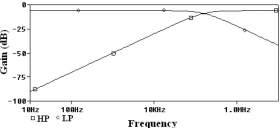
Fig.6. Frequency responses of HP and LP filters
(a)
(b)
Fig. 7. Input signal (a) Time domain representation (b) Frequency spectrum
(b)
Fig.8. HP Filter (a) Transient response (b) frequency spectrum.
(a)
(b)
Fig.9. LP Filter (a) Transient response (b) Frequency spectrum.
Fig.10. AP filter (a) Phase and magnitude Responses (b) Transient responses
5. Conclusion
A new single CDBA based current mode first order multi function filter topology is presented. The configuration can be used to synthesize lowpass, highpass filter functions. The allpass function can also be included with the use of programmable switches. The proposed theory is verified using SPICE simulations.
References
[1] Biolek D., Senani R., Biolkova V., Kolka Z. (2008) : Active Elements for Analog Signal Processing: Classification, Review, and New Proposals. Radioengineering, 17, pp. 15-32.
[2] Acar C., Ozuguz S. (1999) : A new versatile building block: current differencing buffered amplifier suitable for analog signal processing filters. Microelectronics Journal, 30, pp.157-160.
[3] Ozcan S., Kuntman H., Cicekoglu O. (2002) : Cascadble current mode multipurpose filters employing current differencing buffered amplifier (CDBA). International Journal of Electronics and Communications (AEU), 56, pp. 67-72.
[4] Keskin A. U. (2004) : Cascade approach for the realization of high ordervoltage-mode filters using single CDBA-based first and secondsections. Journal of RF-Engineering and Telecommunications, 58, pp.188-194.
[5] Keskin A. U. (2005) : Voltage-mode high-Q band-pass filters and oscillatorsemploying single CDBA and minimum number of components. International Journal of Electronics, 92, pp.479-487.
[6] Keskin A. U. (2006) : Multi-function biquad using single CDBA. Electrical Engineering, 88, pp. 353–356.
[7] Pisitchalermpong S., Pukkalanun T., Tangsrirat W., Surakampontom W. (2005) : Current Differencing Buffered Amplifier Based Multiple-output Biquadratic Filters. Proc. of IEEE Conference on Electron Devices and Solid-State Circuits, pp. 521-524.
[8] Nandi R., Venkateswaran P., Das S., Kar M. (2010) : CDBA-based electronically tunable filters and sinusoid quadrature oscillator. Journal of Telecommunication, 4, pp.35-41.
[9] Tangsrirat W., Surakampontom W., Fujii N. (2003) : Realization of Leap frog filters using current differencing buffered amplifiers. IEICE Trans. Fundamentals, E86-A, pp.318-326.
[10] Acar C., Sedef H. (2003) : Realization of nth-order current transfer function using current differencing buffered amplifiers. International Journal of Electronics, 90, pp.277-283.
[11] Maheshwari S. (2007) : Voltage-mode all-pass filters including minimum component count circuits. Active and Passive Electronic Components, vol. 2007, doi:10.1155/2007/79159 5 pages.
[12] Kacar F., Ozcelep Y. (2011) : CDBA Based Voltage-Mode First-Order All-pass Filter Topologies,” IU-JEEE 11, pp.1327-1332. [13] Lahiri A. (2009) : Comment on Voltage-Mode All-Pass Filters Including Minimum Component Count Circuits. Hindawi Publishing
Corporation Active and Passive Electronic Components vol. 2009 doi:10.1155/2009/595324, 4 pages.
[14] Toker A., Ozoguz S.R., Cicekoglu O., Acar C. (2000) : Current-Mode All-Pass Filters Using Current Differencing Buffered Amplifier and a New High Bandpass Filter Configuration. IEEE Trans, on circuits and systems—ii: analog and digital signal processing, 47, pp. 949-954.