Effect of CuI Anode Buffer Layer on the Growth of
Polymers Thin Films and on the Performances of Organic
Solar Cells
*
Pedro Pablo Zamora1, Fernando Raul Díaz1#, Maria Angelica del Valle1, Linda Cattin2, Guy Louarn2, Jean Christina Bernède3
1Facultad de Química, Pontificia Universidad Católica de Chile, Santiago, Chile; 2Institut des Matériaux Jean Rouxel (IMN), Centre National de la Recherche Scientifique, Université de Nantes, Nantes, France; 3MOLTECH, Centre National de la Recherche Scientifique, Université de Nantes, Nantes, France.
Email: #[email protected]
Received November 29th, 2012; revised January 6th, 2013; accepted January 21st, 2013
ABSTRACT
Organic photovoltaic cells using polymer belonging to the aniline-heteroaryl family as electron donor have been achieved by thermal evaporation. We show that the properties of the polymer film, morphology, molecule order and conductivity depend strongly on the bottom anode buffer layer. While cells without anode buffer layer or with MoO3 or
CuI anode buffer layer have been probed, we show that CuI allows improving strongly the cells efficiency through an improvement of the morphology and conductivity of the polymer film. This shows that although it is necessary a good band matching at the interface, this is not sufficient, because the templating effect of CuI on the polymer film is primor- dial for photovoltaic cells improvement.
Keywords: Organic Solar Cells; Vacuum Thermal Evaporation; Conjugated Polymers; Aniline-Heteroaryl Polymers
1. Introduction
Conjugated organic polymers have been of great interest as an important class of electronic materials because of their high electrical conductivities [1]. Polyaniline is one example which has received a great interest and has been employed in a number of commercial applications [1-4], however, it has no photovoltaic properties due to inade- quate band gap for these applications. On the other hand, furan and thiophene are two of the five-membered het- eroaromatic ring compounds that have been extensively studied in terms of its reactivity, its specific physicoche- mical properties, and its technological applications [5-10]. It has attracted particular attention, due to its low band gap value, notwithstanding due to high oxidation poten- tial, difficulty which many authors have overcome by changing the substituents in furan and thiophene rings. In addition, various, co-polymers and biopolymers [11-13] based on polyfuranes and polythiophenes show good sta- bility.
Furan/aniline and Thiophene/aniline based polymers, as poly 4-(2-furanyl)-aniline (P4,2FA) and poly 4-(3- furanyl)-aniline (P4,3FA) 4-(2-thiophenyl)aniline (P4,2TA) and 4-(3-thiophenyl)aniline (P4,3TA), will exhibit a re-
duced Eg. Consecuently these are materials with photo- electrical properties which could be employed in solar cells. Along with this it is possible to study the effect of different anode buffer layers in the photovoltaic yield when these polymers are used as electron donor in pho- tovoltaic devices.
Organic photovoltaic is nowadays one of the most in- vestigated research field, because of low cost and low temperature process [14]. Smart chemistry can design conjugated polymeric structures for organic photovoltaic cells (OPVCs) and progress has been made in recent years. Nevertheless, most of the materials designed today suffer from the disadvantage of low carrier mobility, which limits the short circuit current of the cells and therefore their efficiency. To solve this problem, differ- ent approaches, such as thermal annealing or additives, have been used to improve the carrier mobility. A well know mean consists in the increase of the order present in the layer. The fundamental structure of OPVCs con- sists in the photoactive layer sandwiched between two electrodes [15]. The photoactive layer can be a bilayer of an electron donor (ED), and an electron acceptor (EA) or a bulk heterojunction consisting of a blend of the two types of organic semiconductors. Indium tin oxide (ITO) is commonly used as transparent conductive anode. In
order to increase the anode work function, which is nec- essary for efficient hole collection, the ITO surface is subjected to specific treatments, such as oxygen plasma, or coated with a suitable anode buffer layer [16]. Metal, such as gold [17], but also transition metal oxides [18], such as tungsten oxide [19], molybdenum ox- ide MoO
3
[20] and nickel oxide
WO3
NiO
[21] have been used as efficient anode buffer layer (ABL). If a lot of works have been dedicated to the improvement of the band matching at the interface anode/organic electron donor, no many works have been devoted to the possibi- lity of templating the organic layer through the use of specific anode buffer layer. As a matter of fact it has been already shown that, in the case of small molecules, it is possible to modify the molecular orientation of the organic layer through the use of specific anode buffer, such as PTCDA [22], CuI [23-25]. In the present study, we show that this result can be generalized to polymers.Two technological routes are mainly used to grow OPV cells, the deposition of polymers and nanoparticles from solution by spin coating technique and the vacuum sublimation of small molecules and oligomers [26]. The former route has given the concept of bulk heterojunction solar cells (BHJ) [27], while the later gives the multi- heterojunction solar cells family [28]. Compared to spin coating deposition, sublimation under vacuum allows easy purification of organic material. High purity is cri- tical not only for devices performances, but also for long device life time. In addition, vacuum deposition allows facile fabrication of multilayered devices and facile con- trol of the layers thickness [29]. Moreover the templating effect of the substrate, if present, on the organic film structure is amplified by the vacuum deposition process, since in that case the organic material is deposited mole- cule by molecule onto the substrate. Recently, the vac- uum thermal evaporation of poly (3-hexylthiophene) (P3HT) for application in photovolataic cells has been demonstrated [30,31]. In the present work we widen the field of application of the CuI as templating anode buffer layer to polymers deposited by vacuum sublimation. In order to put in evidence this effect of CuI on the growth of different organic film, we investigated multi-hetero- junction solar cells. We show that for different polymers belonging to the aniline-heteroaryl family, a thin CuI buffer layer allows to enhance strongly the OPV cells performance through the improvement of the conductiv- ity of the organic donor, via improvement of the optical absorbance and structural properties of these polymers.
2. Experimental
The chemical syntheses of monomers was made by Su- zuki-Miyaura cross coupling between 4-bromoaniline and the heteroaryl boronic acid , respectively, in presence of 10 mol% Pd C as catalyst and potassium carbonate.
Subsequently, the monomers were purified and polymer- ized using H5IO6 and HClO4 as oxidizing agent mixture
[32]. The polymers were dedoped using a solution of NH4OH (pH = 9) for 24 h under stir.
The characterizations of monomers and polymers
structures were carried out using NMR and UV-vis spec- troscopy. NMR spectra were recorded on a Bruker 400 MHz spectrophotometer using DMSO d6 as deuterated
solvent UV-Vis measurements were carried out on a
CARY 5G spectrophotometer.
In the present work, OPVCs studied were the multi- heterojunction: ITO ABL ED C60 BCP Al . In these cells, fullerene
C60 and BCP (bathocuproine) have been used as electron acceptor and exciton blocking layer (EBL), respectively. C60 is well known as a very efficientelectron acceptor. Between the C60 and the aluminium
cathode, the introduction of EBL improves significantly the OPV cells performances [33]. The ABL was either CuI, MoO3 [34] or MoO CuI3 . Also OPV Cells without
[image:2.595.311.535.559.709.2]ABL have been probed as reference. The different ED used were Poly(4-(2-thiophenaniline)) (P4,2TA), Poly (4-(2-furanylaniline)), (P4,2FA), Poly(4-(3-thiophenani- line)) (P4,3TA) and Poly(4-(3-furanylnaniline)), (P4,3FA) the schemes of these different polymers are presented in
Figure 1.
Before thin films deposition, the ITO coated glass substrate was scrubbed with soap, rinsed with distilled water, dried and next placed in the vacuum chamber
10 Pa4
. The ABL, ED, C60, BCP layers were deposited
onto the substrate by sublimation and Al were deposited by high vacuum evaporation, without breaking the vac- uum. The CuI layer thickness was 3 nm, in the light of earlier works [23], while the MoO3 layer was 4 nm thick
[35]. The thickness of the different ED layers has been optimized experimentally. It is, whatever the ED used, 15 nm. Finally, the thickness of the ED, C60, and BCP films
was 15 nm, 40 nm and 9 nm respectively. The deposition
H N
S
n
S H
N
n
(a) (b)
S H
N
n
S H
N
n
(c) (d)
rate of the organic material was 0.05 nm s. The effect-
tive area of each cell was 0.16 cm2. The thin films thick- nesses and deposition rates were estimated quartz monitor. Finally, the cell arrangement was: in situ using a
60
glass ITO 100 nm ABL ED C 40 nm BCP 9 nm Al 100 nm
All the chemical products have been provided by Al- drich except for the ED, which have been synthesized in the Pontificia Universidad Católica de Chile, while the ITO glass coated have been provided by SOLEMS, France. The chemical products form Aldrich were used without any purification, the monomer synthesized were purified by chromatography column and crystallization then were polimerizated and used as ED in the OPV (a new purification occurred) Indeed, it has been shown that, using the same charge in the evaporation crucible, there is an “auto purification” of the product [36].
In order to try to prevent polymer degradation during deposition, we have measured the temperature of the evaporation boat, using a copper-constantan thermocou- ple, the weld of the thermocouple being clamped be- tween the body of the crucible and its lid. The thin films structures were analyzed by X ray diffraction (XRD) by a Siemens D5000 diffractometer using Kα radiation from
.
Ka
Cu 0.15406 nm
The optical measurements were carried out at room temperature using a Carry spectrometer. The film optical density was measured at wavelengths of 1 to 0.30 μm.
AFM images on different sites of the film were taken
ex-situ at atmospheric pressure and room temperature. All measurements have been performed in tapping mode (Nanowizard JPK Instrumens), Classical Silicon-SPM- Sensor were used (NCHR, NanoWorld®). The average
force constant and resonance were approximately 14 N m
and 330 Hz, respectively. The cantilever was excited at its resonance frequency.The surface roughness Rq (root mean square roughness) of each polymeric surface over the different buffer layer was evaluated with AFM soft- ware.
The electrochemical work was performed on a Volta- master model CV 50 W potenciostat/galvanostat, using a conventional three-compartment, three-electrode cell, and a polycrystalline platinum disk (0.07 cm2 geometric area)
as working electrode. The counter electrode was a coiled Pt wire of large area, separated from the electrolytic so- lution by a sintered glass. The reference electrode was a
Ag AgCl electrode that matches the potential of the saturated calomel electrode (SCE). Then all potentials quoted in the electrochemical section, are referred to the SCE. The electro-polymerization of each monomer (0.01 mol·L−1) was carried out in anhydrous acetonetrile using
tetrabutylammonium hexafluorophosphate (TBAPF6, 0.1
mol·L−1) as supporting electrolyte. All the system was
kept under argon atmosphere and all measurements were
performed at room temperature.
Electrical characterizations were performed with an automated I-V tester, in the dark and under sun global AM 1.5 simulated solar illumination. Performances of photovoltaic cells were measured using a calibrated solar simulator (Oriel 300 W) at 100 mW cm2 light intensity
adjusted with a PV reference cell (0.5 cm2 CIGS solar
cell, calibrated at NREL, USA). Measurements were per- formed at an ambient atmosphere. All devices were illu- minated through TCO electrodes [37].
In order to determine the effect of the ABL on the dif- ferent ED film conductivity, we have investigated the J-V characteristics of hole-only devices with MoO3 or
CuI ABL. These devices were grown using high work- function electrode buffer layers. The hole only devices were fabricated with high work function MoO3, which is
well known to be a hole injector (collector) and a block- ing electron layer. Hole only devices have been made using the same ITO covered glass substrate than those used to grow OPV cells. After deposition of the ABL, an ED film thick of 15 nm has been deposited. Then the organic film has been covered with a MoO3 film thick of
4 nm. Finally aluminium has been used as top electrode. We have also proceeded to thermal gravimetric analy- sis (TGA) of the different EDs to determine changes in weight in relation to temperature, in order to check the stability of the polymers at the temperature used for their sublimation. TGA analyses were carried out in a 951 Thermogravimetric Analyser TA-9900 in nitrogen at- mosphere
flow rate 100 mL min
at a heating rate of 10˚C/min.3. Experimental Results
3.1. NMR Characterization of Monomers and Polymers
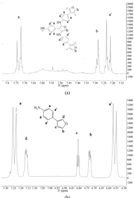
To determine the polymerization positions, the polymers were characterized using NMR spectroscopy. The NMR signal that disappears in the NMR of polymer indicates. the growth position on the chain [38].
P4,2FA shows in both NMR spectra Figure 2 the sig-
signal d is attributed to linkage of furane-furante ring as Lère-Porte et al. have reported previously [38,39]. This results indicates that the polymerization of 4,2FA occurs by carbon 5 of furane ring and exist only one furane- furane linkeage because the linkage Nitrogen-Nitrogen of aniline rings is not possible in this kind of polymerize- tion. In the case of 4,3FA the NMR spectra Figure 3
show that after the polymerization of monomer the sig- nals c and d disappears and the signal b remains which h indicates that the polymerization occurs by two positions of furane ring (carbon 2 and 4) of random forms. This produces a branched polymer without presence of qui- noids units. This fact prevents a decrease of molecular band gap.
In the case of 4,2TA and 4,3TA the same synthetic behavior is observed as previously we have reported [38]. In this sense the positions of polymerization of 4,2TA, 4,3TA, 4,2FA and 4,3FA is the same respectively i.e.
4,2TA and 4,2FA polymerized by position 5 of het- eroaryl ring which produces a non branched polymer. By the other hand 4,3TA and 4,3FA have two positions of
(a)
(b)
Figure 2. 1H-NMR spectra in the aromatic range for (a) the monomer 4,2FA and (b) the polymer P4,2FA.
(a)
[image:4.595.307.538.93.435.2](b)
Figure 3. 1H-NMR spectra in the aromatic range for (a) the Polymer P4,3FA and (b) the monomer P4,3FA.
polymerization (carbon 2 and 4 of heteroaryl ring) which produces a branched structure. The NMR spectra of 4,2TA and 4,3TA have been previously reported by Zamora et al. [38]. These results suggest that in these polymers the Sulfur or Oxygen atoms of heteroaryl ring have no significant influence in the polymerization pro- cess.
3.2.Thermal Gravimetric Analysis and Electrochemical Characterization of the Polymers
Before polymer thin film deposition by sublimation un- der vacuum, the thermal stability of the different poly- mers used has been studied by TGA measurements. The results are presented in Figure 4. It can be seen that the
[image:4.595.59.286.360.705.2]Figure 4. TGA of the different EDs: (a) P4,2TA, (b) P4,3TA, (c) P4,2FA and (d) P4,3FA.
of polymer chains during the deposition process the tem- perature was limited at 190˚C.
On the other hand, in the case of solar cells, after pho- ton absorption and exciton creation, the efficiency of the photo induced charge separation is a key problem. What- ever the structure used, bilayer or bulk heterojunction, the donor and acceptor should have their relative electron affinity (LUMO) and ionisation potential (HOMO) well adapted. The electron affinity of the donor is smaller than that of the acceptor, while the ionisation potential of the acceptor must be significantly greater than that of the donor. When the donor is excited, the electron promoted to the LUMO will lower its energy by moving to the LUMO of the acceptor. The band offset at the organic hetero-interface between the electron-donor material and the electron-acceptor material tends to separate the exci- ton diffusing to that interface into an electron in the ac- ceptor and a hole in the donor material. Therefore, the knowledge of the HOMO and LUMO of the organic ma- terial is very important. When the organic material shows a one electron reversible reduction and oxidation wave, cyclic voltammetry (CV) is recognised as an important technique for measuring band gaps, electron affinities (LUMO) and potential ionisation (HOMO). The oxida- tion process corresponds to removal of charge from the HOMO energy level whereas the reduction cycle corre- sponds to electron addition to the LUMO. Moreover, the potential difference can be used to estimate the energy gap of the polymer. Therefore, the HOMO and LUMO energy of the different EDs used in the present work have been estimated before their use in OPVCs. The energy level of the normal hydrogen elec- trode (NHE) is situated 4.5 eV below the zero vacuum energy level. To estimate the HOMO and LUMO energy, the slope change of the anodic and cathodic current respectively were determined. These values corresponds to the onset oxidation potential on, and onset re- duction potential and correlates linearly with
the HOMO and LUMO energy, with a correction factor of 4.4 eV [40, 41]:
Eg LUMO HOMO
Eox
Ered on
ox on
red on
E HOMO E 4.4 eV
E LUMO E 4.4 eV
The different HOMO and LUMO values deduced from cyclic voltammetry measurement are reported in Table 1,
polymeric responses were assessed applying a perturba- tion to the modified electrode in a monomer-free solution of supporting electrolyte
1
6
0.1 mol L TBAPF in an- hydrous acetonitrile finding in all cases a p-type and n-type doping. No chemical degradation of these states was observed after 10 cycles.
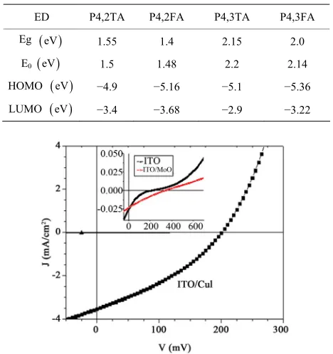
3.3. OPVCs Performances
The performances of the cells using the different EDs are presented in Figure 5, the ABL being used as a parame-
[image:5.595.306.540.408.657.2]ter. Then, in order to understand the different behaviours, the multilayer structures ITO/ABL/ED have been char- acterized by XRD, AFM and optical measurements.
Table 1. Optical (Eg) and electrochemical (E0) band gap of
the different EDs. Their HOMO and LUMO values de- duced from electrochemical measurements are also re- ported.
ED P4,2TA P4,2FA P4,3TA P4,3FA
Eg eV 1.55 1.4 2.15 2.0
E0 eV 1.5 1.48 2.2 2.14
HOMO eV −4.9 −5.16 −5.1 −5.36
LUMO eV −3.4 −3.68 −2.9 −3.22
Figure 5. Typical J-V characteristics of ITO ABL P42TA
60
C BCP AI structure, with ABLITO CuI under illu-
mination of AM1.5 solar simu- lation ( 2
100mW cm . Inset: enhanced J-V characteristics of the cells using ABL without
, 3
.Typical results for the four OPVCs configuration used are presented in Figure 5, in the case of P4,2TA as ED.
The corresponding values of the short circuit currents , open circuit voltages
Jsc
Voc
, fill factors
FF and cells efficiency
are given in Table 2. The cellspresented in each figure have been deposited in the same run. It can be seen that the presence of CuI in the ABL improve strongly the OPVC performances. This im- provement is mainly due to the fact that Jsc is more than one order of magnitude higher in presence of CuI. There is also a significant improvement of FF, while there is no enhancement of Voc Table 2. All these results in a
power cell efficiency (PCE) two orders of magnitude higher when CuI is used as ABL. Even if the overall ef- ficiencies are slightly smaller, the same effect is obtained in the case of P4,2FA (Table 2).
Must be noted that when P4,3TA and P4,3FA are used as ED, the PCE of the cells is very small, however the same improvement in presence of CuI is achieved, from around 2.5 × 10⁻³% and 2 × 10⁻⁴% without CuI to 2.5 ×
10−2% and 3 × 10⁻³% with CuI in the case of P4,3TA and
P4,3FA, respectively. It can be concluded that the solar cell performances are far better when the ITO is recov- ered with CuI. As it can be seen in Table 2, MoO3, in the
case of P4,2TA, improve the OPVC performance and since it is well known that MoO3 allows achieving a
good band matching between the ITO anode and the HOMO of the ED, whatever the HOMO value [42], we have tried to optimise the PCE of the OPVCs using a double ABL, MoO CuI3 in our last samples. One can
see that this double ABL allows improving significantly the PCE.
3.4. Characterization of the ITO/ABL/ED Structures
In order to understand the origin of the strong improve-
Table 2. Photovoltaic performance data under AM1.5 con- ditions of devices using P4,2TA or P4,2FA as ED with dif- ferent anodes.
ED Anode
mA cmJsc 2ment of the OPVCs performances induced by the pres- ence of a CuI ABL, the structures ITO ABL ED , with
3
ABL MoO ,CuI, or no ABL and
ED P4, 2TA, P4, 2FA, P4,3TA, P4,3FA , have been submitted to XRD, AFM, optical and hole only electrical characterizations.
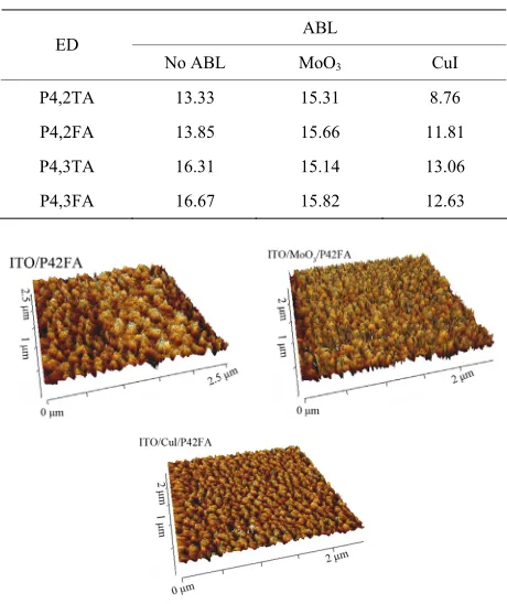
All EDs deposited onto the different ABLs have been studied by XRD diffraction. However, well resolved dif- fraction peaks have been obtained only with P4,2FA. In that case, as it can be seen in Figure 6, the intensity of
the diffraction peaks depends on the ABL used. The presence of CuI induces a significant improvement of the intensity of peaks. Also, some new diffraction peaks are visible. Therefore, the presence of CuI induces, not only an improvement of the crystallinity of the deposited films, but also the presence of two crystalline phases of the organic material or at least two different orientations of the crystallites.
This show that, the CuI ABL has a clear templating effect on P4,2FA, it induces some ordered growth of the organic material. Even if not easily visible in the case of the others EDs, the films being often highly disordered, CuI could also modify the growth properties of the or- ganic films. As a mater of fact, this order modification is corroborated by the AFM study. Indeed, the AFM study shows that, even if the root mean square roughness (Rq) of the surface is not strongly modified by the ABL con- figuration Table 3, the CuI ABL induces a significant
decrease of the Rq value, which results in a clear modi- fication of the surface morphology of the polymer film
Figure 7.
This effect, which in the case of P4,2FA Figure 7 can
be correlated to the modification of the crystalline order in the film, is also clearly visible in the case of the others polymers, as shown for P4,2TA in previous works of Zamora et al. [38]. Therefore it can be inferred that, here also, the order of the organic molecules is modified by
Voc (V) FF (%) η(%) ITO 0.024 0.20 14 6.7 10 43
ITO MoO 0.023 0.34 21 1.6 10 3
ITO CuI 2.55 0.20 33.5 0.17
P4,2TA
3
ITO MoO CuI 4.13 0.20 33 0.23
ITO 0.021 0.42 20 1.7 10 3
3
ITO MoO 0.017 0.47 16.5 1.3 10 3
ITO CuI 0.94 0.47 21 0.10
P4,2FA
3
ITO MoO CuI 0.88 0.36 40.5 0.13 Figure 6. X-ray diffraction diagrams of the ITO/ABL/ P4 2FA, structures with , ,
3
Table 3. Variation of the Rq (root mean square roughness) for the four EDs with the different ABLs.
ABL ED
No ABL MoO3 CuI
P4,2TA 13.33 15.31 8.76
P4,2FA 13.85 15.66 11.81
P4,3TA 16.31 15.14 13.06
P4,3FA 16.67 15.82 12.63
[image:7.595.327.515.409.536.2]
Figure 7. TM-AFM images of P4,2FA, (15 nm thick) depos- ited onto ITO ITO MoO CuI3 and ITO CuI .
the CuI ABL.
The influence of the ABL on the optical absorbance has been probed. From the example of P4,2TA visualised in Figure 8, it can be seen that there is no clear shift of
the absorption spectrum of the film, there is only a slight increase of the absorption in presence of CuI mainly for the small band situated at 440 nm.
The J-V characteristics of the hole only devices are shown in Figure 9. It shows typical curves log (J) against
log (V) plots obtained when injecting holes through the ITO contact. Charge transport in these devices is limited to holes. Electron injection from the aluminium electrode can be neglected, due to the large electron barrier due to the MoO3 interlayer. The devices using CuI and
3
MoO CuI ABL show largest current density at the same driving voltages as compared to the devices using MoO3 ABL. Clearly the conductivity is enhanced by
nearly an order of magnitude when a CuI or MoO CuI3
ABL is used on the place of the MoO3 ABL. For instance
when the applied voltage is 10 mV, the current density with MoO3 ABL is 0.047 mA cm2, while it is
2
0.35 mA cm with CuI ABL.
Therefore, it is clear that the presence of a CuI layer below the organic film induces significant modifications of these organic films, which result in a strong improve-
ment of the solar cells performances in the presence of CuI ABL.
4. Discussion
[image:7.595.347.500.581.707.2]After First of all, following the works of Kovacik et al. and E. Nasybulin et al. [30,31], we have checked the temperature of the polymer crucible in order to avoid polymer molecule destruction during the sublimation. Since the mass loss of P4,2TA is bellow 5% at 190˚C we can conclude that this polymer is not destroyed during the deposition. Moreover, even if there is, probably, some decrease of the molecular weight due to the subli- mation process, this decrease is not sufficient to modify strongly the optical properties of the polymer, since the absorption domain of the films is in good agreement with absorption deduced from the band gap estimated by elec- trochemistry. If this is true for P4,2TA, the case of P4,2FA is different. Actually at 190˚C its weight loss is nearly 5%, which means that there is probably some degradation of the polymer, at least a strong decrease of the chain lengths and/or opening of furan ring. It is know that furan ring is less stable than thiophene ring [43]. When furane ring is opened two ketones units are formed (dicarbonyl moieties). This chemical modification pro-
Figure 8. Variation of the optical density of the ITO/ABL/ P4,2TA structures with the ABL.
duces more flexibility in the polymeric chains and a lost of conjugation due to the decrease of quinoids and het- eroaryl units. Moreover, aniline-thiophene units show more thermal stability in a greater range of temperature due to thiophene ring, which is more aromatic than fu- rane. These degradations of the chain length or furan ring-opening decrease the photovoltaic yield. Therefore P4,2FA films correspond probably to oligomer films. This can explain the crystallization of the films, since films of oligomers crystallize easier than polymer films (Figure 6). Therefore if the partial destruction of the
polymer chain during the heating process of P4,2FA can explain that better PCE are achieved with OPVCs using more stable polymer, the fact that it crystallize more ea- sily help us to put in evidence the effect of the different ABL on the growth properties of the films. When depos- ited onto CuI it is clear that the crystallization of P4,2FA is different from that achieved when it is deposited onto MoO3. The intensity of the diffraction peaks is far higher
than that obtained when the films are deposited onto MoO3, which testifies of a better crystalinity of the films
deposited onto CuI. After decomposition of the strongest diffraction peak of each diagram, it can be seen that the grain size of the crystallites is more or less the same in each films since the full width at half maximum is around 0.20 degree. This means that the ratio crystallized phase/amorphous phase is higher when the film is depos- ited onto CuI. Moreover the new peaks visible in the dif-fraction diagram of the films deposited onto CuI show that a new crystalline phase or at least a new grain orient- tation is induced by the CuI under layer. The different characterizations of the structures ITO ABL ED have shown that CuI modifies the properties of the organic films. The XRD and AFM studies show that the order in the films is significantly improved by the CuI bottom layer. If these modifications have not a broad impact on the optical properties of the films they improve signify- cantly their conductivity. As a matter of fact, if CuI does not induce systematically the crystallization of the poly- mers, it improves the order of the molecules in the films, which justifies the improvement of the conductivity of the films. It is well known that a limiting factor of the PCE in organic OPVCs is the small conductivity of the organic films. Therefore an increase of this conductivity induces higher short circuit current density and therefore better PCEs.
Another important parameter is the open circuit volt- age Voc, it is well known that its maximum value corre- sponds to the difference between the HOMO of the ED and the LUMO of the acceptor. Therefore, following the results indicated in Table 1 the Voc obtained with
P4,2FA must be higher than that achieved with P4,2TA. It can be seen in Table 2 that it is actually the case. How-
ever, the PCE of achieved with the cells using P4,2TA as ED is higher than that achieved with P4,2FA, which is due to the smaller Jsc measured. Such disappointing re- sult must be related to the fact that, as shown by the TGA study, P4,2FA is less stable than P4,2TA and it under- goes probably damages during its deposit.
Nevertheless, whatever the polymer used as electron donor, it is clear that CuI improved strongly the OPVCs performances. Since it is known that a MoO3 anode
buffer layer allows obtaining good band matching with electron donors, which HOMO value is around 5eV [42], it is clear from the present study that if this condition is necessary it is not sufficient in the case of the polymers studied in the present work. He is necessary furthermore to use an anode buffer layer which improves the mor- phology and therefore the conductivity of the polymer. In the present case, we show that CuI is very efficient as templating layer. Theses differences in organic film mor- phology on different substrates are usually attributed to the different interaction between the organic material and the surface of the substrates. Often it is proposed that when the interaction organic molecule-substrate is stronger than the molecule-molecule interaction, the films adopt a lying down configuration (2 dimensions growth of the film). If the molecule-substrate interaction is weak, the molecule-molecule interaction dominates and the mole- cules adopt a standing up configuration (three dimension growth of the film). For instance, different studies have been done on the influence of the substrate on the mo- lecular orientation of CuPc [44,45]. In the present study, we show that the presence of a thin CuI layer onto the ITO allows controlling the morphology of the polymer films. It has been already shown that CuI and other cop- per halides can interact easily with organic molecules [46-49]. For instance, complex formation between CuI and organic molecules leads to different π stacking cop- per halide motifs [46]. More precisely, there is complex formation between copper (I) iodine and nitrogen-donor of the organic molecules. Also, it is well-established that the pymSH/pymS− and bis (2-pyrimidyl)disulfide (pym2S2)
ligands are good coordinating ligands toward soft Lewis acids such as Cu (I) and it as been shown that, the sol- vothermal reactions between pyrimidinedisulfide (pym2S2) and CuI in CH2Cl2:CH3CN lead to the formation of
atoms) when they are in contact.
5. Conclusion
In order to discuss the effect of CuI on the properties of the polymer films and their corresponding OPVCs, cells with CuI and also with MoO3 or without ABL have been
probed. It is shown that the CuI ABL thin film induces significant improvement of the structural properties of the oligomers, which increases the order in the deposited films and allows strong enhancement of the OPVCs per- formances due to possible strong Cu-polymer interaction on the ABL surface like pyrimidine-Cu interaction. By the other hand the EDs show is thermally stable under 190˚C and the rate of degradation does not appear to significantly affect the optical properties of the polymer. The PCE achieved with the better polymer of the four EDs of the aniline-heteroaryl family studied in the pre- sent work is of the same order of magnitude as those achieved by Kovacik et al. and E. Nasybulin et al. [30,31] with the polythiophene, which is very promising and justifies further working with these materials.
6. Acknowledgements
The authors thank FONDECYT financial support through project 1095156. P.Z. acknowledge the doctoral scholar- ship 21090478, doctoral scholarship support 24110046, granted to conduct this research and ECOS CONICYT project No.C09E02
REFERENCES
[1] S. Bhadra, N. Singha and D. Khastgir, “Effect of Aro- matic Substitution in Aniline on the Properties of Poly- anil,” European Polymer Journal, Vol. 44, No. 6, 2008, pp. 1763-1770.
[2] Z. Liu, W. Guo, D. Fu and W. Chen, “p-n Heterojunction Diodes Made by Assembly of ITO/Nano-Crystalline TiO 2/Polyaniline/ITO,” Synthetic Metals, Vol. 156, No. 5, 2006, pp. 414-416.
[3] J. Gao, J. M. Sansinena and H. L. Wang, “Chemical Va- por Diven Polyaniline Sensor/Actuators,” Synthetic Met- als, Vol. 135-136, No. 4, 2003, pp. 809-810.
[4] A. Bishop and P. Gouma, “Leuco-Emeraldine Based Po- lyaniline—Poly-Vinyl-Pyrrolidone Electrospun Compos- ites and Bio-Composites: A Preliminary Study of Sensing Behaviour,” Reviews on Advanced Materials Science, Vol. 3, No. 10, 2005, pp. 209-214.
[5] J. Upadhyay, P. Gaston, A. A. Levy and A. Wassermann “Cationic Polymerisation of a Bicyclopentyl Derivative: Mechanism of Formation of Deeply Coloured, Electri- cally Conducting Polymers,” Journal of The Chemical
Society, Vol. 593, 1965, pp. 3252-3266.
doi:10.1039/jr9650003252
[6] C. F. Blakely, R. J. Gillespie, L. Roubinek, A. Wasser-
mann and R. F. M. White, “Conversion of Cyclopentadi- ene into New Bicyclopentyl Derivatives; Structure De- termination with the Help of Proton Magnetic Resonance Spectroscopy,” Journal of The Chemical Society, Vol. 374, 1961, pp. 1939-1945. doi:10.1039/jr9610001939 [7] J. Upadhyay, J. B. G. Wallace and A. Wassermann, “Pro-
ton Accetor Properties and Electrical Conductance of Deeply Coloured Cyclopentadiene Polymers,” Polymer, Vol. 7, No. 9, 1966, pp. 465-468.
[8] P. V. French, L. Roubinek and A. Wassermann, “Prepara- tion and Properties of Deeply Coloured, Electrically Conducting Polymers,” Journal of The Chemical Society, Vol. 376, 1961, pp. 1953-1963.
doi:10.1039/jr9610001953
[9] M. Armour, A. G. Davies and A. Wassermann, “Colored Electrically Conducting Polymers from Furan, Pyrrole, and Thiophene,” Journal of Polymer Science Part A, Vol. 5, No. 7, 1966, pp. 1527-1538.
[10] C. E. H. Bawn, C. Fitzsimmons and A. Ledwith, “Reac- tivity and Mechanism in the Cationicpolymerization of Isobutyl Vinyl Ether,” Polymer, Vol. 12, No. 2, 1971, pp. 119-140.
[11] M. Talu, M. Kabasakolglu, F. Yildirin and B. Sari, “Elec- trochemical Synthesis and Characterization of Homopo- lymers of Polyfuran and Polythiophene and Bipolymer Films Polyfuran/Polythiophene and Polythiophene/Poly- furan,” Applied Surface Science, Vol. 181, No. 1, 2001, pp. 51-60.
[12] I. Carrillo, E. Sanchez de la Blanca and M. J. Gonzalez- Tejera, “Influence of the Electropolymerisation Time on the Nucleation Mechanism, Structure and Morphology of Polyfurane/Perchlorate Doped Films,” Polymer, Vol. 42, No. 1, 2001, pp. 9447-9453.
doi:10.1016/S0032-3861(01)00500-6
[13] M. Kabasakalo˘glu, M. Talu, F. Yildirim and B. Sari, “The Electrochemical Homopolymerization of Furan and Thiophene and the Structural Elucidation of Their Bi- polymer Films,” Applied Surface Science, Vol. 218, No. 1, 2003, pp. 85-97.
[14] F. C. Krebs, “A Review of Printing and Coating Tech- niques,” Solar Energy Materials & Solar Cells, Vol. 93, No. 4, 2009, pp. 394-412.
doi:10.1016/j.solmat.2008.10.004
[15] J. C. Bernede, “Organic Photovoltaic Cells: History, Prin- ciple and Techniques,” Journal of the Chilean Chemical
Society, Vol. 53, No. 3, 2008, pp. 1549-1564.
[16] A. Godoy, L. Cattin, L. Toumi, F. R. Diaz, M. A del Valle and J. C. Bernede, “Effects of the Buffer Layer In- serted between the Transparent Conductive Oxide Anode and the Organic Electron Donor,” Solar Energy Materials
& Solar Cells, Vol. 94, No. 4, 2010, pp. 648-654.
[17] J. C. Bernède, L. Cattin, M. Morsli and Y. Berredjem, “Ultra-Thin Metal Layer Passivation of the Transparent Conductive Anode in Organic Solar Cells,” Solar Energy
Materials &Solar Cells, Vol. 92, No. 11, 2008, pp. 1508-
1520.
Fullerene Film without Thermal and Solvent Annealing,”
Applied Physics Letters, Vol. 99, No. 14, 2011, pp. 735-
748.
[19] S. Han, S, W. S. Shin, M. Seo and D. Gupta, “Improving Performance of Organic Solar Cells Using Amorphous Tungsten Oxides as an Interfacial Buffer Layer on Transparent Anodes,” Organic Electronics, Vol. 10, No. 5, 2009, pp. 791-797.
[20] M. T. Grenier, M. G. Helander and Z. B. Wang, “Highly Simplified Phosphorescent Organic Light Emitting Diode with >20% External Quantum Efficiency at >10,000cd/ m2v,” Applied Physics Letters, Vol. 96, No. 21, 2010, pp. 213-230.
[21] S. Y. Park, H. R. Kim, Y. J. Kang, D. H. Kim and J. W. Kang, “Organic Solar Cells Employing Magnetron Sput-tered p-Type Nickel Oxide Thin Film as the Anode Buffer Layer,” Solar Energy Materials & Solar Cells, Vol. 94, No. 12, 2012, pp. 2332-2346.
[22] P. Sullivan, T. S. Jones, A. J. Ferguson and S. Heutz, “Structural Templating as a Route to Improved Photo- voltaic Performance in Copper Phthalocyanine/Fullerene (C60) Heterojunctions,” Applied Physics Letters, Vol. 91, No. 23, 2007, pp. 233114-233126.
[23] C. H. Cheng, J. Wang, G. T. Du and S. H. Shi, “Organic Solar Cells with Remarkable Enhanced Efficiency by Using a CuI Buffer to Control the Molecular Orientation and Modify the Anode,” Applied Physics Letters, Vol. 97, No. 8, 2010, p. 83305.
[24] B. P. Rand, B. P. D. Cheyns, K. Vasseur, N. C. Giebink and S. Nothy, “The Impact of Molecular Orientation on the Photovoltaic Properties of a Phthalocyanine/Fullerene Heterojunction,” Advanced Functional Materials, Vol. 22, No. 14, 2012, pp. 2987-2995.
[25] T. M. Kim, J. Kim, H. Shim and J. Kim, “High Efficiency and High Photo-Stability Zinc-Phthalocyanine Based Pla- nar Heterojunction Solar Cells with a Double Interfacial Layer,” Applied Physics Letters, Vol. 101, No. 11, 2012, p. 113301. doi:10.1063/1.4748123
[26] J. C. Bernède, A. Godoy, L. Cattin, F. R. Diaz, M. Mor- sili and M. A. del Valle, “Organic Solar Cells Perform- ances Improvement Induced by Interface Buffer Layers,” 1st Edition, M. D. Rugescu, In Tech, 2 February 2010. [27] P. Kumar and S. Chand, “Recent Progress and Future
Aspects of Organic Solar Cells,” Progress in Photovol-
taics: Research and applications, Vol. 20, No. 4, 2012, pp.
377-415.
[28] P. Peumans and S. R. Forrest, “Very-High-Efficiency Double-Heterostructure Copper Phthalocyanine/C60 Pho- tovoltaic Cells,” Applied Physics Letters, Vol. 79, No. 1, 2001, pp. 126-128. doi:10.1063/1.1384001
[29] W. Zeng, K. S. Yong, Z. M. Kam, F. Zhu and Y. Li, “Ef-fect of Blend Layer Morphology on Performance of ZnPc:C60-Based Photovoltaic Cells,” Applied Physics
Letters, Vol. 97, No. 13, 2012, p. 133304.
[30] P. Kovacik, G. Sforazzini, A. G. Cook, S. M. Willis, P. S. Grant and H. E. Assender, “Vacuum-Deposited Planar Heterojunction Polymer Solar Cells,” Applied Material
Interfaces, Vol. 3, No. 1, 2011, pp. 11-15.
[31] E. Nasybulin, F. Feinstein and M. Cox, “Electrochemi- cally Prepared Polymer Solar Cell by Three-Layer Depo- sition of Poly(3,4-Ethylenedioxythiophene)/Poly(2,2′Bi- thiophene)/Fullerene (PEDOT/PBT/C60),” Polymer, Vol. 52, No. 16, 2011, pp. 3627-3632.
[32] M. Can, S. Uzuna and N. Pekmez, “Chemical Polymeri- zation of Aniline Using Periodic Acid in Acetonitrile,”
Synthetic Metals, Vol. 159, No. 14, 2009, pp. 1486-1490.
[33] S. E. Shaheen and C. J. Brabec, “2.5% Efficient Organic Plastic Solar Cells,” Applied Physic Letters, Vol. 78, No. 6, 2001, p. 841.
[34] L. Cattin, F. Dahou, Y. Lare, M. Morsli, R. Tricot, K. Jondo, A. Khelil, K. Napo and J. C. Bernède, “MoO3 Sur- face Passivation of the Transparent Anode in Organic Solar Cells Using Ultrathin Films,” Journal of Applied
Physic Letters, Vol. 105, No. 3, 2009, p. 34507.
[35] J. Ryu and C. Jang, “Supramolecular Reactor in Aqueous Environment: Aromatic Cross Suzuki Coupling Reaction at Room Temperature,” Journal of Organic Chemistry, Vol. 70, No. 2, 2005, pp. 8956-8962.
[36] R. F. Slazman and J. Xue, “The Effects of Copper Phtha- locyanine Purity on Organic Solar Cell Performance,” Or-
ganic Electronics, Vol. 6, No. 5, 2005, pp. 242-450.
[37] Y. Berredjem, N. Karst, L. Cattin, A. Lakhdar-Toumi, A. Godoy, G. Soto, F. R. Diaz, M. Morsli and J. C. Bernede, “The Open Circuit Voltage of Encapsulated Plastic Pho- tovoltaic Cells,” Dyes and Pigments,Vol. 78, No. 2, 2008, pp. 148-156.
[38] P. P. Zamora, M. B. Camara, I. A. Jessop and F. R. Diaz, “Synthesis, Characterization, Morphology and Photovol- taic Properties of Aniline-Tiophene Based Polymers,” In-
ternational Journal of Electrochemical Science, Vol. 7, No.
7, 2012, pp. 8276-8288.
[39] J. J. Lère-Porte, E. Moreau and C. Torreilles, “Highly Conjugated Poly(Thiophene)s—Synthesis of Regioregu- lar 3-Alkylthiophene Polymers and 3-Alkylthiophene/ Thiophene Copolymers” European Journal of Organic
Chemistry,Vol. 2001, No. 7, 2001, pp. 1249-1258.
doi:10.1002/1099-0690(200104)2001:7<1249::AID-EJO C1249>3.0.CO;2-F
[40] S. Admassie, O. Inganas, W. Mammo, E. Perzon and M. R. Andersson, “Electrochemical and Optical Studies of the Band Gaps of Alternating Polyfluorene Copolymers,”
Syntetic Metals, Vol.156, No. 7, pp. 614-624.
[41] A. Charas, J. Morgado, J. Martinho, L. Alcácer, S. Lim, R. Friend and F. Cacialli, “Synthesis and Luminescence Pro- perties of Three Novel Polyfluorene Copolymers,” Poly- mer,Vol. 44, No. 6, 2003, pp. 1843-1455.
[42] J. C. Bernède, L. Cattin, S. Ouro Djobo, M. Morsil, S. R. B. Kanth, S. Patil, P. Leriche, F. R. Diaz and M. A. del Valle, “Influence of the Highest Occupied Molecular Or- bital Energy Level of the Donor Material on the Effec- tiveness of the Anode Buffer Layer in Organic Solar Cells,” Physica Status Solidi A, Vol. 208, No. 8, 2011, pp. 1989-1994.
Materials and Design, Vol. 32, No. 1, 2011, pp. 238-245. [44] H. Peisert, T. Schweiger, J. M. Auerthammer, M. Kkun-
pfer and M. S. Golden, “Order on Disorder: Copper Ph- thalocyanine Thin Films on Technical Substrates,” Jour-
nal of Applied Physics, Vol. 90, No. 1, 2001, pp. 466-469.
[45] D. Qi, J. Sun, X. Gao and S. Wang, “Large Damage Threshold and Small Electron Escape Depth in X-ray Absorption Spectroscopy of a Conjugated Polymer Thin Film,” Langmuir, Vol. 26, No. 1, 2006, pp. 165-172. [46] A. J. Blake, N. R. Brooks, N. R. Champness, P. A. Cooke
and M. Crew, “Copper(I) iodide Coordination Networks- Controlling the Placement of (CuI)∞ Ladders and Chains
within Two-Dimensional Sheets,” Crystal Engineering, Vol. 2, No. 2, 1999, pp. 181-185.
[47] T. S. Lobana, S. Khanna, A. Castineiras, G. Hundal and Z.
Anorg, “Synthesis of an Unprecedented CuI Polymer with Alternate Cu(μ-S)2Cu and Cu(μ-Cl)2Cu Cores Bridged by Pyridine-2-Carbaldehyde Thiosemicarbazone,” Allgemei-
ne Chemie,Vol. 636, No. 3, 2010, pp. 454-456.
[48] A. Gallego, O. Castillo, C. J. Gómez-García, F. Zamora and S. Delgado, “Electrical Conductivity and Lumines- cence in Coordination Polymers Based on Copper(I)- Halides and Sulfur-Pyrimidine Ligands,” Inorganic Che-
mistry, Vol. 51, No. 1, 2012, pp. 718-727.
[49] S. Li-Sha, W. Qing-Li and N. Yun-Yin, “Syntheses, Structure, and Photoluminescent and Thermal Properties of a Novel Coordination Polymer [CuI(3-bpfob)]n with One-Dimensional Helical Chain,” Synthesis and Reacti-
vity in Inorganic, Metal-Organic, and Nano-Metal Che-