Abstract: This paper presents the optimization of 2-phase interleaved DC-DC boost converter (IBC) in order to achieve switching device losses and current stress reduction. Principally, the distributed of input currents in 2- phase IBC can reduce the current stress on components i.e., inductor and switching devices, consequently the lower rating of inductor and switching device can be considered. However, the interleaving technique does not reduces the inductor current ripple in 2-phase IBC. The comparison of switching device losses and the current stress for conventional DC-DC boost converter (1-phase IBC), 2-phase IBC, and 3-phase IBCs are provided in this paper. The 180-degree phase-shifted pulse width modulation technique (PWM) is implemented on the 2-phase IBC. The results show that by increasing the phase number of IBCs, 1-phase, 2-phase and 3-phase, the switching device losses are reduced i.e., 76 mW, 30 mW, and 22 mW, respectively. Meanwhile, the inductor current stresses is reduced as well, i.e., 0.8 A, 0.4 A, and 0.27 A, respectively. The finding shows the conduction loss decreases when the phase number of IBC increases. However, this will increases the switching loss of the IBC. Thus, the 2- phase IBC is selected as the optimum phase of IBC with regards to the switching loss and conduction loss consideration of the semiconductor devices.
Keywords: Multiphase IBC, interleaving technique, current stress, current ripple, semiconductor loss, conduction loss
© Universiti Tun Hussein Onn Malaysia Publisher’s Office
IJIE
Journal homepage: http://penerbit.uthm.edu.my/ojs/index.php/ijie
ISSN : 2229-838X e-ISSN : 2600-7916
The International
Journal of
Integrated
Engineering
Optimum Phase Selection of Multiphase Interleaved DC-DC
Boost Converter for Current Stress and Switching Devices
Losses Reduction
A. N. Kasiran
1, A. Ponniran
1,*, N. A. S. Ngamidun
1, M. S. Shaili
1, A. M. Zaini
1,
M. H. Yatim
11Faculty of Electrical and Electronic Engineering
Universiti Tun Hussein Onn Malaysia, Malaysia
*Corresponding Author
DOI: https://doi.org/10.30880/ijie.2019.11.01.002
Received 13 March 2018; Accepted 18 November 2019; Available online 30 April 2019
1.
Introduction
Iin
Vin Cout
S Vout
I1 L1
Iin
Vin S1 S2
Cout
Vout
D1
of circuit structure, the input current is evenly distributed to each branch of the multiphase circuit branches which the reliability of circuit is improved to be more efficient. Theoretically, the reduction of conduction loss can be achieved due to an even current sharing and current stress between phases at the input side. Besides, the multiphase IBC is an attractive option for high power and high current applications with low current ripple [11]. The 2-phase IBC has shown the optimum phase for switching device losses and current stress reductions at the components by considering the specifications in this paper. Thus, the performance of the 2-phase IBC is observed for switching device losses and current stress reductions. The comparison of conventional DC-DC boost converter and 3-phase IBC also provided in this paper.
2.
Principle of Conventional and 2-phase Interleaved DC-DC Boost Converters
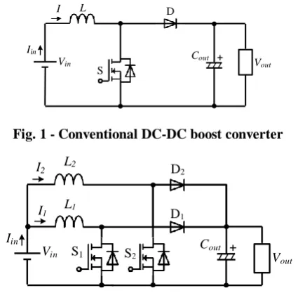
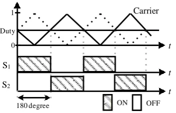
Basically, the conventional DC-DC boost converter consists of one diode (D), one switch (S), an input inductor (L) and a capacitor (C) at the output side, Fig. 1. Meanwhile, in 2-phase IBC circuit structure consist of two diodes, two switches, two input inductors, and a capacitor, Fig. 2. Generally, the circuit structure of conventional DC-DC boost converter suffered high switching device losses due to the limitation of circuit structure, Fig. 1. Practically, high current stress at the input side caused the selection rating of inductor is high and costly. However, the unique feature of 2-level IBC circuit structure able to reduce the current stress at the inductor and switching devices, consequently low rating of inductor can be selected and switching device losses reduction can be achieved.
I L D
Fig. 1 - Conventional DC-DC boost converter
I2 L2 D2
Fig. 2 - 2-phase interleaved DC-DC boost converter (IBC)
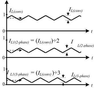
Fig. 3 shows the operation modes of 2-phase IBC that operates in interleaving operation. Fig. 4 shows 180 degree of phase shifted pulse width modulation (PWM) for the switching device in 2-level IBC. The operation shows the phases operate in interleaved where the phase delay is shifted after another. The phase-shifted for each phase is expressed as follows,
360
n
(1)Iin
I2 L2
I1 L1
Vin S1
D2
D1
S2
Cout
Vout
Iin
I2 L2
I1 L1
Vin S1
D2
D1
S2 Cout V
out
(i) (ii)
1 Carrier
Duty
0 t
S1
S2
t
t
180 degree ON OFF
Fig. 4 - 180-degree phase shifted PWM of 2-phase IBC
3.
Parameters Design of Conventional and 2-phase Interleaved DC-DC Boost Converters
Tables 1 shows the specification of conventional DC-DC boost converter and 2-level IBC are considered in this paper. Principally, the inductor current ripple is considered in order to design inductor. Basically, the continuous conduction mode is considered in this paper. In DC-DC boost converter design, continuous conduction mode is the most preferred operation mode for high power application over the discontinuous conduction mode. This is because the continuous conduction mode has an advantage of lower conduction loss and smaller current stress on the semiconductor devices [12]. Thus, the minimum inductance for the converter circuit in continuous conduction mode and the output capacitance of the converter can be expressed as follow,D
1D
2 R Lmin 2 fsw
(2)
C D out
Rf r (3)
where R is the resistance, fsw is the switching frequency, r is the voltage ripple factor. The output voltages of the
converters are controlled independently by varying the duty cycle D. Meanwhile, the output voltage Vout and boost ratio
β of the conventional DC-DC boost converter and 2-phase IBC can be expressed as follow,
Vout
1
1 D Vin (4)
1 1 D
Vout
Vin
(5)
3.1
Current Stress and Input Current Ripple Reductions
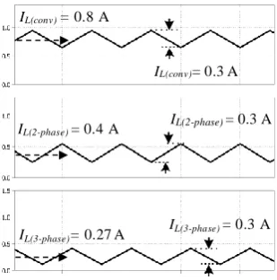
Input current ripple is occurred due to the switch are turn-ON and turn-OFF which produce ripple. The input current ripple must be considered according to the application which required small current ripple at the input side. Usually, the input current ripple reduction can be achieved by considering a large input inductor. However, this will increases the size and weight of the converter [13]. Thereby, an interleaving technique is considered where the input current ripple reduction can be achieved by summation of all phases of current ripples. Fig. 5 shows the principle of input current ripple reduction when interleaving technique is applied. By increasing the phase number of IBC, input current ripple is reduced significantly. Fig. 6 shows the current stress of each phase is reduced with similar inductor current ripple when the phase number of IBC is increased. Thus, this condition can easily be written as follows:
∆Iin(3-phase) < ∆Iin(2-phase) < ∆Iin(conv) (6)
IL1(3-phase) < IL1(2-phase) < IL(conv) (7)
R
2
1 IL(conv)
IL(conv)
0 t
1
IL1(2-phase) = (IL(conv))÷2 I
L(2-phase)
0 t
1
I
0
L1(3-phase) = (I L(conv) )÷3 I L(3-phase)
t
∆IL1(3-phase) = ∆IL1(2-phase) = ∆IL(conv) (8)
Input current (A)
Iin(conv)
Iin(2-phase)
Iin(3-phase)
Time (s)
Fig. 5 - Input current ripple reduction of multiphase IBC
Fig. 6 - Reduction of current stress in conventional DC-DC boost converter, 2-phase IBC and 3-phase IBC
3.2
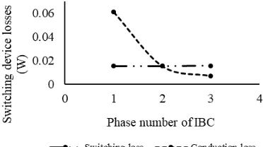
Switching Device Losses Reduction
There are mainly two kinds of losses that occurred in switching devices which are conduction loss and switching loss [14]. Generally, the conduction loss and the switching loss of MOSFET are expressed as follow, respectively,
Pcond(m) Ids on D (9)
I V
t t
Psw(m)
ds ds r
6
fsw (10)Conduction loss Pcond is proportionally to the squared of drain-source current Ids. Thus, the conduction loss is
significantly decreased when drain-source current is decreased. These can be achieved when interleaving technique is applied by increasing the phase number. Meanwhile, the diode only consists of conduction loss Pcond(d) which depends
on forward rms current If(rms) where it considers the maximum and minimum current of diode.
Pcond(d ) I f (rms ) Vf (1 D) (11)
However, this paper only considered MOSFET conduction loss in the analyses. Fig. 7 shows the relationship between conduction loss and switching loss against the phase number of IBC. It shows that the conduction loss is decreases when the phase number of IBC is increased. Meanwhile, the switching loss is increases as the phase number
f
Iin
DT
Iin
Conduction loss Switching loss
Optimum phase of IBC
IL(conv) = 0.8 A
IL(conv)= 0.3 A
IL(2-phase) = 0.4 A
IL(2-phase) = 0.3 A
IL(3-phase)= 0.27 A
IL(3-phase) = 0.3 A
of IBC increasing. Thus, an optimum phase of IBC must be considered in order to achieve high efficiency of converter. From the illustrations, the optimum phase number of IBC is occurred when the conduction loss and switching loss is across each other. Besides, it depends on the output power of converter.
Phase of IBC, n
Fig. 7 - Losses against phase number of IBC
4.
Results and Analysis
The specifications of the simulation and experimental works is shown in Table 1. The MOSFET considered in the experimental is SPW21N50C3
Table 1 - Specifications of conventional DC-DC boost converter and 2-phase IBC
Parameters Value
Output voltage, Vout (V) 60
Switching frequency, fsw (kHz) 200
Duty cycle, D 0.5
Voltage ripple factor, r (%) 1
Resistor, R (Ω) 150
Inductor, Lconv = L(2-phase) (mH) 1
Output capacitor, Cout (µF) 1200
Output power, Pout (W) 24
4.1
Current Stress Reduction
By considering interleaving technique, the current stress reduction on inductor is achieved. The current stress of conventional DC-DC boost converter, the 2-phase IBC, and the 3-phase IBC are observed. Fig. 8 shows the simulation results of the inductor current stresses on conventional DC-DC boost converter, 2-level IBC and 3-level IBC, respectively. Meanwhile, Fig. 9 shows the simulation results where the current stresses reduction is achieved at MOSFET of the 2-phase IBC and 3-phase IBC.
Fig. 8 - Simulation result of current stress on inductor
S
w
it
c
h
in
g
d
e
v
ic
e
l
o
ss
e
s,
Ids(conv)= 0.80 A
Ids(2-phase)= 0.40 A
Ids(3-phase)= 0.27 A
Input Voltage (V) Vin= 30 V
0, Vin Output Voltage (V) V
out= 60 V
0, Vout
Inductor Current (A) IL= 0.3 A
0, IL(conv)
IL(conv)-ave = 0.8 A
Vin/Vout(50 V/div), IL(conv)(200 mA/div)
10 (µs/div)
Fig. 9 - Simulation result of current stress on switching device (MOSFET)
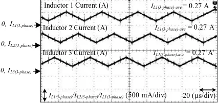
The principle of DC-DC boost converter is to boost-up from low input voltage to high output voltage. The output voltage is boost-up depending on the duty cycle D. For the experimental specifications, the selected input voltage is 30 V and the output voltage is then boost-up to 60 V with 50% of duty cycle. Figs.10, 11 and 12 show the current stress on inductor for the conventional, the 2-phase IBC and the 3-phase IBC. It is experimentally confirmed that the inductor current stress for each phase is decreased when the phase number of IBC is increased.
Fig. 10 - Input voltage, output voltage and inductor current stress/ripple of the conventional DC-DC boost converter
Input Voltage (V) Vin= 30 V
0, Vin
Vin(25 V/div), IL1(2-phase)/IL2(2-phase)(200 mA/div)
Inductor 1 Current (A) IL1 = 0.3 A
0, IL1(2-phase)
0, IL2(2-phase)
IL1(2-phase)-ave = 0.4 A
Inductor 2 Current (A)
IL2(2-phase)-ave = 0.4 A
IL2= 0.3 A
10 (µs/div)
Fig. 11 - Input voltage and the current stress/ripple of the 2-phase IBC
0, IL1(3-phase)
0, IL2(3-phase)
Inductor 1 Current (A)
Inductor 2 Current (A)
Inductor 3 Current (A)
IL1(3-phase)-ave = 0.27 A
IL1(3-phase)-ave = 0.27 A
IL1(3-phase)-ave = 0.27 A
0, IL3(3-phase)
IL1(3-phase)/IL2(3-phase)/IL3(3-phase) (500 mA/div) 20 (µs/div)
4.2
Input Current Ripple and Current Reduction
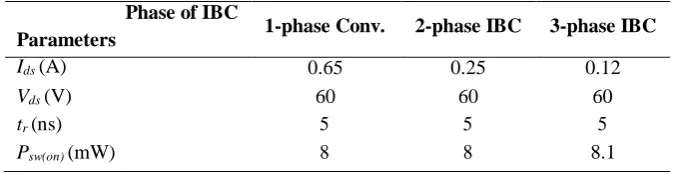
Conduction loss occurred when there is conduction current or energy dissipated by components in a circuit while MOSFET is turn-ON. As discussed at previous sections, the conduction loss is decreased as the phase number of IBC is increasing. Meanwhile, switching loss occurred during transition of turn-ON and turn-OFF for some periods of time. Thus, the switching loss will be increased as the phase number of IBC increases where proportionally to the number of switching devices used. Several data are recorded in analyzing the losses occurred in switching devices. Tables 2 and 3 show the switching loss of MOSFET during turn-ON, Psw(on) and turn-OFF, Psw(off). Meanwhile, Table 4 shows the
conduction loss in MOSFET and Table 5 shows the total losses of MOSFETs for the conventional DC-DC boost converter, 2-phase IBC and 3-phase IBC. Meanwhile, Fig. 13 shows the relationship between switching device losses and phase number of IBC based on the analyses in this study. It can be observed that the 2-phase IBC has the optimum of switching loss and conduction loss as compared to the 1-phase conventional boost converter and the 3-phase IBC based on the switching device losses characteristic as shown in Fig 7. Thus, the optimum phase of IBC with the load considered in this paper is 2-phase IBC.
Table 2 - Dissipated energy during turn-ON Phase of IBC
Parameters 1-phase Conv. 2-phase IBC 3-phase IBC
Ids (A) 0.65 0.25 0.12
Vds (V) 60 60 60
tr (ns) 5 5 5
Psw(on) (mW) 8 8 8.1
Table 3 - Dissipated energy during turn-OFF Phase of IBC
Parameters 1-phase Conv. 2-phase IBC 3-phase IBC
Ids (A) 0.95 0.55 0.42
Vds (V) 60 60 60
tr (ns) 4.5 4.5 4.5
Psw(on) (mW) 7.20 7.20 7.29
Table 4 - Conduction loss in MOSFET Phase of IBC
Phase of IBC Ids (A) Rds(on) (Ω) D Pcond (W)
1-phase Conv. 0.8 0.19 0.5 0.061
2-phase IBC 0.4 0.19 0.5 0.015
3-phase IBC 0.27 0.19 0.5 0.007
Table 5 - Switching devices losses Phase of IBC
Phase of IBC Psw (mW) Pcond (mW) Pmosfet (mW)
1-phase Conv. 15 61 76
2-phase IBC 15 15 30
Fig. 13 - Switching device losses in MOSFET against phase number of IBC
5.
Conclusion
In this paper, it is concluded that the switching device losses and current stress at the components are able to be reduced with considered 2-phase IBC by implementing the multiphase circuit structure and interleaved technique. Due to the unique features of the multiphase IBC circuit structure, it reduces the selection rating of the components, conduction loss and the failure rate of the converter. However, the additional of switching devices cause the switching loss increases. Thus, by concerning in this issue, the optimum phase of IBC must be considered in order to obtain the lowest of the switching and conduction losses. By referring the semiconductor losses, the optimum phase of IBC is 2- phase as discussed at the Section 4.2. The volume and size reduction of the inductor in the 2-phase IBC can be considered in the future due to the unique feature of the circuit structure.
References
[1] A. B. Ponniran, K. Orikawa, and J. Itoh, “Minimum Flying Capacitor for N-Level Capacitor DC/DC Boost Converter,” IEEE Trans. Ind. Appl., vol. 52, no. 4, pp. 3255–3266, 2016.
[2] A. Ponniran, K. Orikawa, and J. Itoh, “Modular multi-stage Marx topology for high boost ratio DC/DC converter in HVDC,” in 2015 IEEE International Telecommunications Energy Conference (INTELEC), 2015, pp. 1–6.
[3] A. Ponniran, K. Orikawa, and J. Itoh, “Fundamental Operation of Marx Topology for High Boost Ratio DC-DC Converter,” IEEJ J. Ind. Appl., vol. 5, no. 4, pp. 329–338, 2016.
[4] A. B. Ponniran, K. Orikawa, and J. i. Itoh, “Interleaved high boost ratio Marx topology DC-DC converter,” in 2015 IEEE 2nd International Future Energy Electronics Conference (IFEEC), 2015, pp. 1–6.
[5] M. A. Harimon, A. Ponniran, A. N. Kasiran, and H. H. Hamzah, A Study on 3-phase Interleaved DC-DC Boost Converter Structure and Operation for Input Current Stress Reduction, vol. 8. 2017.
[6] A. Bakar, A. Ponniran, and T. Taufik, Simulation and Analysis of Multiphase Boost Converter with Soft- Switching for Renewable Energy Application, vol. 8. 2017.
[7] P. Nandankar and J. P. Rothe, “Design and implementation of efficient three-phase interleaved DC-DC converter,” in 2016 International Conference on Electrical, Electronics, and Optimization Techniques (ICEEOT), 2016, pp. 1632–1637.
[8] K. Kroics, U. Sirmelis, L. Grigans, and V. Brazis, “Digitally controlled 4-phase interleaved DC-DC converter with coupled inductors for storage application in microgrid,” in 2015 9th International Conference on Compatibility and Power Electronics (CPE), 2015, pp. 504–509.
[9] M. Maalandish, S. H. Hosseini, S. Ghasemzadeh, E. Babaei, R. S. Alishah, and T. Jalilzadeh, “Six-phase interleaved boost dc/dc converter with high-voltage gain and reduced voltage stress,” IET Power Electron., vol. 10, no. 14, pp. 1904–1914, 2017.
[10] P.-W. Lee, Y.-S. Lee, D. K. W. Cheng, and X.-C. Liu, “Steady-state analysis of an interleaved boost converter with coupled inductors,” IEEE Trans. Ind. Electron., vol. 47, no. 4, pp. 787–795, 2000.
[11] L. Ni, D. J. Patterson, and J. L. Hudgins, “High Power Current Sensorless Bidirectional 16-Phase Interleaved DC-DC Converter for Hybrid Vehicle Application,” IEEE Trans. Power Electron., vol. 27, no. 3, pp. 1141– 1151, 2012.
[12] D. D.-C. Lu, D. K.-. Cheng, and Y.-S. Lee, “A single-switch continuous-conduction-mode boost converter with reduced reverse-recovery and switching losses,” IEEE Trans. Ind. Electron., vol. 50, no. 4, pp. 767–776, 2003. [13] S. Lee and H. Do, “Zero-Ripple Input-Current High-Step-Up Boost–SEPIC DC–DC Converter With Reduced
Switch-Voltage Stress,” IEEE Trans. Power Electron., vol. 32, no. 8, pp. 6170–6177, 2017.