National Conference on Advances in Engineering and Applied Science (NCAEAS) 16th February 2017
In association with
I
nternational
Journal
of
Scientific
Research in
Science and
Technology
Multilevel Inverters : Comparison of Various Topologies and its
Simulation
Mithilesh Shivankar, Komal Deshmukh, Akshay Sahu, Abhijit Dutta
Department of Electrical, Dr. Babasaheb Ambedkar College of Engineering and Research, Nagpur, Maharashtra, India
ABSTRACT
The multilevel inverters have drawn a tremendous interest in power industry now a day for high power and medium voltage energy control applications. Multilevel inverter is used to reduce the harmonic content in output waveform without decreasing the inverter power output. This paper presents the basic but important topologies diode-clamped inverter (N- point clamped), Capacitor clamped (flying capacitor) and Cascaded h-bridge with separated dc sources. This paper also includes advantages and disadvantages of multilevel inverters over conventional inverters along with its working principle and constructional features. The switching sequence of 3 level and 5 level for single leg of above mentioned topologies has been presented in this paper with their waveforms. The designs have been simulated in MATLAB/SIMULINK and the total harmonic distortion (THD) for voltage output has been carried out and comparison of DCMLI, FCMLI and CHB MLI is also done. Emerging topologies like asymmetric hybrid cells and modified cascade h-bridge multilevel inverters with reduced number of switches are also discussed.
Keywords : Multilevel Inverters (MLI), Diode Clamped Inverter (DCMLI), Flying Capacitor Multilevel Inverter (FCMLI), Cascade H-Bridge Inverter, hybrid multilevel inverter, modified cascade h-bridge multilevel inverter, THD
I.
INTRODUCTION
The device which converts dc input voltage to ac output voltage with desired magnitude and frequency, is known as inverter. It is a power electronics device. In practice, inverter gives square wave output voltage waveform while output voltage waveform of the ideal inverter should be sinusoidal. To get better waveform with low harmonic distortion, multilevel inverter are used. Multilevel inverter are starts with a level of three. The concept of multilevel inverter (MLI) has been introduced since 1975[1].
There are several advantage to multilevel approach as compared to conventional two level approach. The smaller voltage steps lead to the production of higher power quality waveforms and also reduce voltage (dv/dt) stress on the load and the electromagnetic compatibility concerns which ultimately results in output with reduced harmonics
Another important feature of multilevel converters is that the semiconductors are wired in a series-type connection, which allows operation at higher voltages. However, the series connection is typically made with clamping diodes, which eliminates overvoltage concerns. Furthermore, since the switches are not truly series connected, their switching can be staggered, which reduces the switching frequency and thus the switching losses. One clear disadvantage of multilevel power conversion is the higher number of semiconductor switches required. It should be pointed out that lower voltage rated switches can be used in multilevel converter and, therefore, the active semiconductor cost is not appreciably increased when compared with the two level cases. However, each active semiconductor added requires associated gate drive circuits and adds further complexity to the converter mechanical layout.
Isolated voltage sources may not always be readily available, and series capacitors require voltage balancing [2].
II.
METHODS AND MATERIAL
Voltage Source Multilevel Inverters has been broadly classified in to two parts depending upon the number of voltage sources as shown below:
A. INVERTER TOPOLOGIES
The basic and most important three topologies of a voltage source multilevel inverters are as follows:
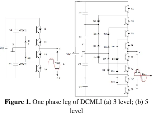
1) Diode Clamped Inverter: Diode Clamped Inverter is also termed as Neutral Point Clamped inverter. In Diode clamped inverter diode is used as a clamping device to clamp the dc bus voltage so as to achieve steps in output voltage. Thus the main concept of this inverters is to use diodes to limit the power devices voltage stress.
A three level single leg diode clamped inverter is shown in figure 1(a) in which dc bus voltage consists of two series connected bulk capacitors C1 & C2, along with four IGBT. The middle point of two capacitor ‘n’ can be termed as neutral point. The output is taken across phase (a) and neutral point (n) as shown in fig below.
Figure 1. One phase leg of DCMLI (a) 3 level; (b) 5 level
For voltage level Van = Vdc/2 turn on the switches S1 and S2, for voltage level Van = 0 turn on the switches S2 and S3, and for voltage level Van = 0 turn on the switches S2 and S3, and for voltage level Van = -Vdc/2 turn on switch S3 and S4.
Similarly a five level single leg diode clamped inverter can be achieved as shown in fig.1 (b). In which the dc bus consists of four capacitors C1, C2, C3 and C4 along with eight IGBT. The output is taken across phase (a) and neutral (n).
To synthesize 5-level output phase voltage, switching sequence as given in table below:
Table 1: Switching table for 5 level DCMLI
An n-level inverter needs (n-1) voltage sources, 2(n-1) switching devices and (n-1) (n-2) clamping diodes. But n becomes sufficiently large then the no. of diodes make the system impractical to implement, which in fact limits the possible no. of levels with such configuration.
capacitor involves series connection of capacitor clamped switching cells, this topology has a ladder structure of dc side capacitors where the voltage on each capacitor differs from that of the next capacitor. The voltage increment between two adjacent capacitor leg gives the size of the voltage steps in the output waveform.
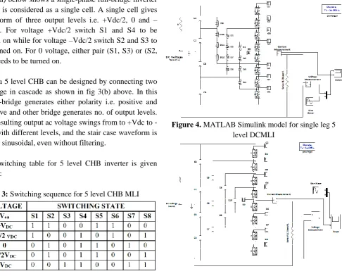
Figure 3. One phase leg of CHB (a) 3 level; (b) 5 level
Fig 3(a) below shows a single-phase full-bridge inverter which is considered as a single cell. A single cell gives waveform of three output levels i.e. +Vdc/2, 0 and – Vdc/2. For voltage +Vdc/2 switch S1 and S4 to be turned on while for voltage –Vdc/2 switch S2 and S3 to be turned on. For 0 voltage, either pair (S1, S3) or (S2, S4) needs to be turned on.
Thus a 5 level CHB can be designed by connecting two h-bridge in cascade as shown in fig 3(b) above. In this one h-bridge generates either polarity i.e. positive and negative and other bridge generates no. of output levels. The resulting output ac voltage swings from to +Vdc to -Vdc with different levels, and the stair case waveform is nearly sinusoidal, even without filtering.
The switching table for 5 level CHB inverter is given below:
Table 3: Switching sequence for 5 level CHB MLI
The relation between number of H-bridges and the associated number of output levels can be given as follows:
III.
RESULTS AND DISCUSSION
The model for single leg 5 level multilevel inverter has been simulated in MATLAB/ SIMULINK for resistive load (RL = 10 ohms).
A. Simulation Results
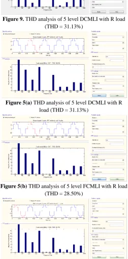
The MATLAB Simulink model for Diode clamped 5 level inverter, Flying Capacitor and Cascade h-bridge inverter has been simulated and is as follows. The 5 level voltage output and current output for R load is as follows:
Figure 5. MATLAB Simulink model for single leg 5 level FCMLI
Figure 6. MATLAB Simulink model for single leg 5 level CHBMLI
Figure 7. 5 level Voltage Output for R load
Figure 8. 5 level Current Output for R load
The voltage and current output for all three inverters are almost same and consists of 5 levels (i.e. +Vdc, +1/2 Vdc, 0, -1/2Vdc. –Vdc). Hence only voltage output and current output of only Cascade H-Bridge inverter is shown in this paper.
B. Results of FFT Analysis
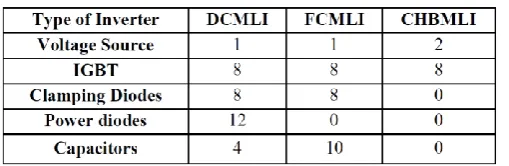
Fast Fourier Transformation (FFT) technique is used for analysis of harmonic content present in the output of multilevel inverter. In this paper FFT analysis is done with resistive load for 3 levels and 5 levels DCMLI, FCMLI and CHBMLI respectively.
FFT analysis gives magnitude of output voltage and Total Harmonic Distortion (%).
THD is calculated as follows:
THD analysis of above mentioned three topologies have been done and are as follows:
Figure 9. THD analysis of 5 level DCMLI with R load (THD = 31.13%)
Figure 5(a) THD analysis of 5 level DCMLI with R load (THD = 31.13%)
Figure 5(c) THD analysis of 5 level CHB MLI with R load (THD = 28.37%)
Thus it can be seen that cascade H-Bridge THD is least of all i.e. 28.37.
C. Comparison of Power components Requirement
The comparison of power component requirements per phase leg among three multilevel inverters is shown below in table 4.
Table 4: Comparison of power component
The THD analysis and comparison of above three topologies has been compared for 5 level output which is shown in TABLE 5 below:
Table 5: Comparison of THD analysis
IV.
CONCLUSION
This paper provides a brief summary of multilevel inverter and its basic three circuit topologies (i.e. Diode Clamped, Flying Capacitor and Cascade H-bridge). Although this paper cannot cover all the detailed work, but the basic principle of different multilevel inverters has been covered. Comparison of topologies is also done in this paper in which cascade H-Bridge multilevel inverter is found to be better than other inverters in such a way that the number of levels can be increased easily by increasing the number of H-Bridge. Also according to constructional point of view Cascade H-bridge Multilevel Inverter (CHBMLI) is very simple. There is no requirement of voltage clamping diodes and voltage balancing diodes which make circuit bulky and increase the cost.
Further inverter circuits can be modified reducing the number of switches and using a single source for more number of output levels (i.e Modified H-Bridge and Hybrid Multilevel Inverter with different gate control strategies for reducing the harmonic contents.
V.
REFERENCES
[1]. T., J. Rodríguez, J. L.Lai, and F. Z. Peng, "Multilevel Inverters: A Survey of Topologies, Controls and Applications". IEEE Trans. Ind. Electronics, vol. 49, no. 4, pp. 724-738, August 2002.
[2]. Nupur Mittal, Bindeshwar Singh, S.P Singh, Rahul Dixit, and Dasharath Kumar, "Multilevel Inverters: A Literature Survey on Topologies and Control Strategies" IEEE Trans on Conference on Power, Control and Embedded Systems, 978-1-4673-1049-9-2012.
[3]. Tejas M. Panchal, Rakesh A. Patel and Hiren S. Darji, "Simulation of Cascaded and Modified Cascaded H-Bridge Multilevel Inverter for 3-Phase Asynchronous Motor", Int.J.of Recent Trends in Engineering and Technology, Vol.11, June 2014. [4]. Liu Wenhua, Member, IEEE, Yan Gangui, Chen
Yuanhua, Zhang Xincheng, Han Yingduo, "A Genric PWM Control Method for Flying Capacitor Inverter.
[5]. A. T. Al Sakhen, A. M. Qasim, B. Qaisieh and A. Elnady, "Experimental and Simulation Analysis for the 5-level Diode Clamped Inverter".
[6]. Asst. Prof. Hamdy A. Ashour Prof. Yasser G. Dessouky, Eng. Samia A. Mahmoud, "OPERATION CONTROL OF MULTILEVEL INVERTERS FOR INDUCTION MOTORS". Arab Academy for Science and Technology, Department of Electrical and Computer Control Engineering Miami, P.O. Box: 1029, Alexandria, EGYPT