A New Approach of Area Efficient High Speed
1024 FFT/IFFT Processor
G.Ravi Kishore1, B.Sangeetha2
1
Associate Professor, 2M Tech Student, ECE Department, Vidya Jyothi Institute of Technology (VJIT)
Abstract: This paper proposes A new approach of area efficient high speed 1024 FFT/IFFT Processor. This processor utilizes 28% of complex multipliers with reduced area. These processors have flexibility of different Fast Fourier Transform sizes (2, 4,8,16,3,64,128,256 and 512) of length, So that the Hardware complexity reduced. The proposed mixed radix butterfly units can be designed in MATLAB SIMULINK. These processors verified by XILINX HDL tool modified with VERILOG language and implemented in 45-nmCMOS technology. The synthesis results shows that are a reduce by 19% and achieve a high throughput rate up to27.5GS/s at 530 MHz In addition, the processor can support for any FFT sizes by addition of stages and works for inverse Fast Fourier Transform by simply taking conjugation of Fast Fourier Transform.
Keywords: Fast Fourier Transform (FFT), Mixed Radix Multipath Delay Commutator (MRMDC), Butterfly Unit (BU), Throughput, verilog.
I. INTRODUCTION
FFT is an important part in OFDM systems. OFDM has been used as a leading modulation technique for wireless and wire line communication standards, such as IEEE 802.11n/ac/ad [1], IEEE 802.15.3.C [2],DAB [3],ultra wide-band UWB[6], and optical OFDM[7][8].High speed OFDM systems such as wireless personal area networks(WPANS [2], UWB[6] and O-OFDM [7],[8] require high speed FFT computations to meet higher data rates. The FFT Computation of real input samples be in 1-4, gives the symmetry property of FFT to reduce the computational complexities in different area of applications like medical in electrocardiography [5]. The FFT processors proposed with real time processing requirements and less hardware complexity[s6].To achieves less area, memory based architectures[7] like application-specific instruction set processors meet the computation of FFT but they can not reach high-speed requirements. For high throughput rate, There are many pipelined architectures proposed[2]-[4].pipelined architures are divided into single path delay commutator [4],single path feedback [5],[6],multipath delay feedback or commutator [12]-[13]. The MDC architectures[7]-[12] are a high throughput and used multiple data paths to maintain easy synchronization control. The radix -4 MDC architures improve the area by reducing of complex multipliers from three to one in ech stage. To perform twiddle factor multiplications in one stage leads one clock cycle, another multiplication needs one more clockcycl faster than the system[31]. Therefore, the architecture in[31] may not used as high speed applications. To get high throughput rate, FFT architectures using folding transformations[32],[33]have proposed.
For high speed applications, processors requires a through put rate of over 2 GS/s,radix-8or radix-16 algorithms are used. Normally, the FFT size is a power of two, for typical like 128 ,256 ,512 and 1024 FFT sizes are not powers of eight. that is radx-8 algorithms cannot handle these FFT sizes. To provide these requirements, the proposed 1024 FFT processor meets the ofdm requirements by using mixed radix algorithm. therefore the proposed processors can perform FFT computations for sizes of not powers of eight. A brief interpretation on the128/256,256/512–point MRMDC pipelined FFT processors with eight parallel data paths can operate on high clock frequency. To maintain the demands of OFDM systems, three types MRMDC architectures are proposed [35]. shred multiplier of 1024 -point eight parallel MRMDC FFT processor have Type 1 reduces the number of butter flying units(BU’s in the first stage. Type 2 proposes the shared multiplier of 1024 processor can reduce the complex multipliers for radix-8 BU’s in the second stage. Type 3 combines both the Type 1 and Type 2 can reduce the number of BU’s and complex multipliers.
II. MIXED-RADIXFFTALGORITHM
The N-point discrete Fourier transform (DFT is defined as X(k) =∑ x(n) W N nk,k=0,102,N-1;n=0,1,2,N-1; (1)
Where x(n ) is the input sequence, X(k) is the output sequence, and Nis the transform length. WNnk denotes the Nth primitive root of
unity, with its exponent evaluated modulo N and is expressed as WNnk = e-j(2Πnk/N )= cos(2Πnk/N) – sin(2Πnk/N ). (2)
N=256
n = 64n1+n2, 0≤n1≤4,0≤n2≤64
k = k1+4k2, 0≤k1≤4, 0≤k2≤64 (3)
Substituting (3) in (1) X (k) = X (k1+4k2) (4)
=∑x(64n1+n2) W256(64n1+n2) (k1+4k2) ;0<n1<4;0<n2<64
=∑ {BF4(n2,k1)}W64n2k2;n2=0,1, . . . . ,63. (5)
The 256 point mixed radix FFT algorithm can be derived from (4) by decomposing the remaining 64-point DFT into 8-point DFT twice.
The MRMDC architecture is explained using 128/256-point MRMDC FFT/IFFT processor .The architecture consists of BU’s, delay commutators, and twiddle factor multipliers. In the first stage, the radix-2/4 BU can perform one radix-4 or two radix-2 operations to compute the 128 and 256-point FFTs. There are three stages based on radix-2, radix-4, and radix-8 algorithms. The input sequence of single path is divided into eight data paths.
III. EXISTING 128-POINT MRMDC FFT/IFFT PROCESSOR
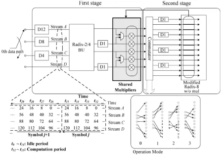
[image:3.612.63.514.319.636.2]The proposed FFT processor can support the 128-point FFT/IFFT in a similar manner to compute the 256-point FFT described in Section . As shown in Fig. 2, the proposed structure reduces the number of BUs from two to one in the first stage compared with the existing structure in Fig. 3. In Fig. 2, the input sequence of each data path is split into four data streams, and
Fig. 1. SMSS based 128/256 point FFT Processor
It takes 12 cycles using D4, D8, and D12 to start the first butterfly computation and four cycles to perform the radix-2/4 operations.
To finish the radix-2 computation using one radix-2/4 BU, the proposed structure requires four cycles. Therefore, the first stage of
the proposed processor also requires 16 cycles, even with one radix-2/4 BU. Thus, the structure consisting of one radix-2/4 BU in
the first stage can reduce the hardware complexity without increasing the number of clock cycles compared with the existing
(a) (b)
(c)
Fig2 : Existing first stage of the zeroth data-path for the 256-point FFT
(a)Reducing the number of butterflies (Type I)
(b)Reducing the number of complex multipliers (Type II)
(c)Architecture employing the scheduling scheme (Type III)
In the first stage in Fig. 2, the radix-2/4 BU can perform two radix-2 butterfly computations. The proposed structure performs complex multiplications for the second stage before the delay commutator using the shared multipliers. The com- mutator is
configured by the operation mode. In the 128-point FFT, the operation mode number is calculated by t modulo four. The
commutator operates in four different operation modes for performing the 128-point FFT. Fig. 3 shows the proposed first stage in
the dotted box shown in Fig. 1, which consists of the input buffer, butterfly processing element, and commutator. In the first stage,
the input sequence of each data path is divided into four data streams (A, B, C, andD), which are delayed by the delay elements to synchronize proper cycles. The butterfly opera- tions in the first stage are performed by four data streams. The output data of the
first stage are delivered to the second stage through the delay elements and the delay commutator by the operation modes .
The FFT size determines the delay cycle of each delay element and the butterfly operation of the first stage. Moreover, the switching of the multiplexers, MUX1, MUX2, and MUX3, depends on the FFT size regardless of whether the data on the same path are to be delayed or not. The control signals of the delay elements vary with the FFT size, and each delay element has different operation modes depending on the FFT size.
The input data multiplied by the appropriate twiddle factors are fed into the second stage for the radix-8 butterfly operation through
the delay commutator, as shown in Fig. 1. In the second stage, the remaining radix-8 calculation without multiplications is performed because all the multipliers of the second stage in the existing one are moved to the shared multipliers in the proposed first
stage. A suitable structure is required to ensure the correction of the FFT output data because the third stage in Fig. 1 is different from the second stage. All the output data generated by the radix-8 butterfly in the second stage are fed to the third stage by a
specific order
where in3 and out2 represent the input data of the third stage and the output data of the second stage, respectively. In (13), p and l represent p =0,1,...,P−1 andl = 0,1,...,L−1, respectively.
P is the number of parallel data paths and L is the number of outputs from a parallel data path.
The proposed processor has the eight-parallel paths, and each path has eight- parallel data streams (A,...,H). The radix-8 BU operates in the third stage using the input sequence from the second stage based on (13). In the existing architecture, the second stage consists of the radix-8 BU in [16] that requires 11 complex multipliers. The third stage using the radix-8 BU also requires 11 complex multipliers. Therefore, the existing architecture requires a total of 22 complex multipliers. In contrast, the proposed architecture requires five multipliers and 11 multipliers in the first stage and the third stage, respectively. Therefore, the proposed architecture in Fig. 3 has 5 multipliers, while the existing architecture requires 22 multipliers for each data path. The proposed MRMDC in Fig. 1 has a total of 128 (16× 8) multipliers because the processors have eight- parallel data paths, whereas the existing architecture requires 176 (22×8) multipliers.
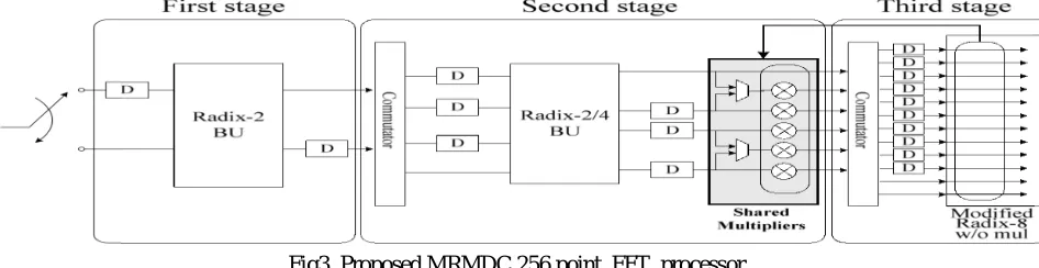
IV. PROPOSED1024-POINTFFTPROCESSOR
This subsection presents the proposed MRMDC 1024-point FFT processor. Fig 3shows the proposed processor that consists of four stages. The radix-2 BUs in the first stage are added to support the 512-point FFT compared with that shown in Fig. 1. The second, third, and fourth stages are the same, as shown in Fig. 1. The processor shown in Fig. 3 performs the 256-point FFT, which is similar to the 256-point FFT in Fig.3.
Fig3. Proposed MRMDC 256 point FFT processor
[image:5.612.71.544.301.423.2]the input sequence is split into eight-parallel data paths that are delayed to arrange the input data order in the first stage. Fig. 3 shows one data path of the existing and proposed structures for the 1024-point FFT, respectively .all the multipliers of the third stage are moved to the shared multipliers in the second stage as we proposed in Type III. The SMSS shown in Fig. 3 can also be applied to the 1024-point FFT. To perform the 1024-point FFT, the proposed structure computes twiddle factor multiplications for the second stage using the shared multipliers on each parallel data path. By employing SMSS, the proposed processor can support both the 256- and 512-point FFTs. In addition, the proposed MRMDC can be applied to larger-size FFTs, such 2048, and 4096, using additional stages. For example, the 2048-point FFT processor consists of one radix-4 BU, the shared multipliers, one radix-8 BU without multipliers, and two radix-8 BUs.
V. RESULTS
The multiplexer, radix 2,and radix 2/4 and modified radix-8BU can be designed in MATLAB Simulink as shown in figures 4,5and 6.
Fig.5.Radix-2/4 BU.
Fig.6. Modified Radix-8 BU.
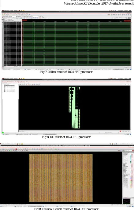
Fig 7. Xilinx result of 1024 FFT processor
[image:9.612.97.535.45.732.2]Fig 8. RC result of 1024 FFT processor
VI. COMPARISONS
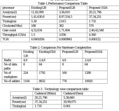
Table 1.Performance Comparison Table
processor Existing128 Proposed128 Proposed 1024
Area(mm2) 11,82,099 3,56,810 20,21,796
Power(uw) 1,41,630.8 8,97,534.5 37,34,251
Timing(ns) 5.30 2.615 1.735
Clockrate(Mhz) 188 382 570
Gate count 4,52,634 1,71,804 2,40,43,548
Throughput (GS/s) 1.5 3.056 4.560
TGR 0.0001856 0.0009961 0.000152
Table 2. Comparison For Hardware Complexities Existing
128
Existing1024 Proposed128 Proposed1024
Radix 4,8 2,4,8 4,8 2,4,8
No of data paths
8 64 8 64
No of multipliers
224 1792 160 1280
No of adders 1104 8832 776 10920
Table 3 . Technology wise comparision table
VII. CONCLUSION
In this thesis report we proposed A Shared Multiplier For Effectual Area Of 1024 Point Fast Fourier Transform Processor. This processor utilizes 28% of complex multipliers with reduced area. This processors have flexibility of different fast fourier transform sizes (2,4,8,16,3,64,128,256 and 512) of length, So that the hardware complexity reduced. The proposed mixed radix butterfly units can be designed in MATLAB SIMULINK. This processors verified by XILINX HDL tool modified with VERILOG language and implemented in 45-nm CMOS technology. The synthesis results shows that area reduce by 19% and achieve a high throughput rate up to 27.5GS/s at 530 MHz. In addition, the processor can support for any FFT sizes by addition of stages and works for inverse fast Fourier transform by simply taking conjugation of fast Fourier transform.
In addition the proposed architecture can apply any FFT size greater than 256 point using additional stages.
REFERENCES
[1] S.-J. Huang and S.-G. Chen, “A green FFT processor with 2.5-GS/s for IEEE802.15.3c (WPANs),” in Proc. Int. Conf. Green Circuits Syst., Jun. 2010, pp. 9– 13.
[2] P.-Y. Tsai, T.-H. Lee, and T.-D. Chiueh, “Power-efficient continuous flow memory-based FFT processor for WiMax OFDM mode,” in Proc. Int. Symp. Intell.Signal Process. commun. Syst., Dec. 2006, pp. 622–625.
[3] X. Guan, Y. Fei, and H. Lin, “Hierarchical design of an application specific instruction set processor for high-throughput and scalable FFT processing,” IEEETrans. Very Large Scale Integr. (VLSI) Syst., vol. 20, no. 3, pp. 551–563, Mar. 2012.
[4] S. He and M. Torkelson, “Designing pipeline FFT processor for OFDM (de)modulation,” in Proc. Int. Symp. Signals, Syst., Electron., Sep. 1998, pp. 257–262. [5] C.-H. Yang,T.-H.Yu, and D.Markovic,’’Power and area optimization of reconfigurable FFT processors: A 3Gpp-LTE example,’’ IEEE Trans. Very
Large Scale Integr. (VLSI) Syst., vol. 47, no. 3, pp. 757–768, Mar. 2012.
[6] T. Cho and H. Lee, “A high-speed low-complexity modified radix-25 FFT processor for high rate WPAN applications,” IEEE Trans. Very Large Scale Integr.
(VLSI)Syst., vol. 21, no. 1, pp. 187–191, Jan. 2013.
[7] C. Chung, S. Wang, and C. Li, “Area-efficient architectural design of radix-4 pipeline fast Fourier transform processor,” in Proc. Workshop Consum. Electron. Signal Process., Nov. 2004, pp. 1–4.
Cadence(180nm) Cadence(45nm)
Area(mm2) 20,21,796 5,38,660
Power(uw) 37,34,251 20,99,075
[8] E. J. Kim and M. H. Sunwoo, “High speed eight-parallel mixed-radix FFT processorfor OFDM systems,” in Proc. IEEE Int. Symp. Circuits Syst., May 2011, PP. 1684–1687.
[9] EunJiKum, Jea Hack Lee ,Myuang Hoon Sunwoo , “Novel Shared Multiplier Scheduling Scheme for Area-Efficient FFT/IFFT Processors” IEEE Trans. Very Large Scale Integr. (VLSI) Syst., vol. 23, no.9, pp. 1689–1699, sep. 2015.
[10] Harpreet Singh Dhillon, AbhijitMitra, “A Digital Multiplier Architecture using UrdhvaTiryakbhyam Sutra of Vedic Mathematics”,IIT-G , pp-1- 4,2010. [11] S.-J. Huang and S.-G. Chen, “A high-throughput radix-16 FFT processor with parallel and normal input/output ordering for IEEE 802.15.3c systems,”
IEEETrans. Circuits Syst. I, Reg. Papers, vol. 59, no. 8, pp. 1752–1765, Aug. 2012.
[12] E. J. Kim and M. H. Sunwoo, “High speed eight-parallel mixed-radix FFT processor for OFDM systems,” in Proc. IEEE Int.Symp. Circuits Syst., May 2011, PP. 1684–1687.
[13] K.-J. Yang, S.-H. Tsai, and G. C. H. Chuang, “MDC FFT/IFFT processor with variable length for MIMO-OFDM systems,” IEEE Trans. Very Large Scale Integr.(VLSI) Syst., vol. 21, no. 4, pp. 720–731, Mar. 2013.
[14] M. Ayinala, M. Brown, and K. K. Parhi, “Pipelined parallel FFT architectures via folding transformation,” IEEE Trans. Very Large Scale Integr. (VLSI) Syst., vol.20, no. 6, pp. 1068–1081, Jun. 2012
[15] M. Garrido, K. K. Parhi, and J. Grajal, “A pipelined FFT architecture for real-valued signals,” IEEE Trans. Circuits Syst. I, Reg. Papers, vol. 56, no. 12, pp.2634–2643, Dec. 2009.