International Journal of Emerging Technology and Advanced Engineering
Website: www.ijetae.com (ISSN 2250-2459, ISO 9001:2008 Certified Journal, Volume 5, Issue 9, September 2015)
301
Implementation of Reliable Power and Delay Efficient
Reconfigurable Multiprecision Multiplier
K.Tanuja
1, Dr. R.Ramana Reddy
21M.Tech, Dept of ECE, MVGR College of Engineering, Vizianagaram, A.P, India. 2Professor, Dept of ECE, MVGR College of Engineering, Vizianagaram, A.P, India.
Abstract—Multiplication is the basic arithmetic operation in Digital Signal Processing (DSP). The accuracy of multiplier signifies the performance of embedded systems, computer graphics, gaming and DSP. Critical factors for designing the multipliers are area of chip, power and speed of multiplication. In this paper, a low power and delay efficient reconfigurable Multiprecision (MP) multiplier is proposed. The MP multiplier is configured with variable precision, Parallel Processing (PP) and dedicated MP operands scheduler to target the optimum performance in various operating conditions. The multiplier is strategically configured with the dynamic voltage and frequency management system along with the Lookup Table (LUT) which replaces the legacy stack of razor flip-flop and voltage scaling unit to achieve Power Efficiency. The MP multiplier consists of Frequency Scaling Unit (FSU) to operate at desired frequency and the Input Operands Scheduler (IOS) which arranges the input data to determine the optimum voltage and frequency for minimal power consumption. In this paper, 64 X 64 bit reconfigurable MP multiplier is proposed using Dadda tree structure, which is delay efficient when compared to the fixed width and reconfigurable multiplier i.e., implemented by Wallace Tree. Power reduction is achieved in the range of 7.48% and 4.82% by implementing 32 bit MP multiplier by Wallace and Dadda Tree respectively. Delay is reduced by 13.17% by implementing Dadda Tree over Wallace Tree. Designing of multiplier is achieved through Xilinx synthesis tool while power analysis is done through XPower Analyzer.
Keywords— Dadda Tree, Digital Signal Processing (DSP), Frequency Scaling Unit (FSU), Finite Impulse Response (FIR), Input Operands Scheduler (IOS), Lookup Table (LUT), Multiprecision (MP), Parallel Processing (PP), Wallace Tree.
I. INTRODUCTION
Multipliers play a significant role in today‘s digital signal processing and numerous other applications. Addition and multiplication is the basic arithmetic operations for high performance systems such as DSPs and Microprocessor. According to statistical reports, Micro-processor and DSP algorithms perform addition and multiplication operation for more than 70% instructions. So these operations dominate the execution time.
The principle of multiplication is mainly two parts i.e., computation of partial products and accumulation of those partial products. Of these, multipliers perform one of the most recurrent arithmetic operations [1]. This switching activity can be extenuated by balancing internal paths through the combination of a transistor level and architectural level optimization techniques [2], [3]. The internal path delays and dynamic power reduction can be achieved by monitoring the effective dynamic range of the input operands, so as to deactivate the unused sections of the multiplier [4], [5] and truncate the output product at the cost of reduced precision [6]. This is possible because in most sensor applications, the real inputs do not always occupy the entire magnitude of its word-length.
International Journal of Emerging Technology and Advanced Engineering
Website: www.ijetae.com (ISSN 2250-2459, ISO 9001:2008 Certified Journal, Volume 5, Issue 9, September 2015)
302
II. EXISTING SYSTEM
Today‘s application specific integrated circuits (ASICs) and full-custom DSPs are designed for a fixed maximum word-length. Therefore, an unnecessary switching activity and power loss is inevitable when 8-bit multiplication computed on a 32-bit Booth multiplier. Various works are intended to implement for word length optimization and to take advantage of the lower energy consumption of the smaller circuit, the pair of input is routed to the smallest multiplier that can compute the result.
8-bit multiplier is reused for the 16-bit multiplication, ‗Share and reuse the structure‘ concept [8] was adopted, adding scalability without large area penalty. To further improve the multiplier‘s performance this method is extended by implementing pipelining. To provide higher precisions and reconfigurability several multiplier elements are grouped together [9]. This analysis has shown that around 10%–20% of extra chip area is needed for 8–16 bits multipliers. Combining Multiprecision (MP) with dynamic voltage scaling (DVS) can provide a dramatic reduction in power consumption by adjusting the supply voltage according to circuit‘s run-time workload rather than fixing it to cater for the worst case scenario. The actual performance of the multiplier running under scaled voltage has to be characterized to guarantee a fail-safe operation, by adjusting the supply voltage.
III.STRUCTURE OF MPMULTIPLIER AND OPERATION
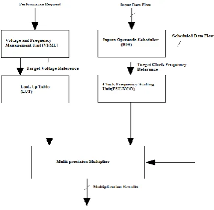
The MP multiplier structure consists of five basic building blocks as shown in Figure 1.
1) Multi precision (MP) multiplier.
2) Input Operands Scheduler (IOS), it is used to reorder the input data into a buffer, for reducing the required power supply voltage transitions.
3) Frequency Scaling Unit (FSU) implemented using a Voltage Controlled Oscillator (VCO). It is used to generate the required operating frequency of the multiplier.
4) Voltage Scaling Unit (VSU) implemented using a voltage dithering technique, Used to limit overhead of silicon area. Its function is to dynamically generate the supply voltage so as to minimize power consumption. It mainly consists of LUTs.
5) Dynamic Voltage/Frequency Management Unit (VFMU) which receives user requirement and control the LUT and FSU by giving suitable voltage and frequency for proper operation of MP multiplier.
Parallel Processing can be used to reduce the supply voltage or increases the throughput. This multiplier comprises nine 8 X 8 bit reconfigurable multipliers. These building blocks can either work as nine independent multipliers or to perform one, two or three 16 X 16 bit
multiplications or a single 32 X 32 bit operation.
In designing the conventional MP multipliers Booth radix-4 Wallace Tree structure is used. In designing the Proposed MP multiplier Dadda Tree Structure is used. However, because of its larger size, the 32 X 32 bit fixed width multiplier exhibits an irregular layout with complex interconnects. This limitation of tree multipliers can be addressed by this MP 32 X 32 bit multiplier, which uses more regular design to partition, regroup, and sum partial products.
A. Lookup Table(LUT)
Field Programmable Gate Arrays (FPGAs) provide a new approach to Application Specific Integrated Circuit (ASIC) implementation that features both large scale integration and user programmability. In FPGA, the connections are implemented in the field using the user programmable routing network.
A FPGA is an integrated circuit designed to be configured by a customer or a designer after manufacturing, hence it is field-programmable. The FPGA configuration is generally specified by using a hardware description language (HDL). FPGAs consist of large resources of logic gates and RAM blocks to implement complex digital computations. FPGAs contain programmable logic components called configurable logic blocks and reconfigurable interconnects that allow the blocks to be wired together. Configurable logic blocks have logic cells and it consists of 4 input look up tables used to implement various functions.
International Journal of Emerging Technology and Advanced Engineering
Website: www.ijetae.com (ISSN 2250-2459, ISO 9001:2008 Certified Journal, Volume 5, Issue 9, September 2015)
[image:3.595.63.281.148.362.2] [image:3.595.73.284.401.576.2]303
Figure 1. Multiplier system architectureFigure 2. Possible configuration modes of MP multiplier
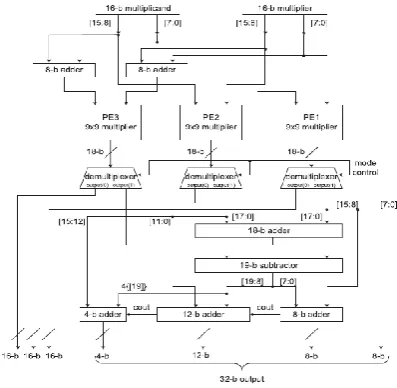
B. Properties of Multi Precision and Re-configurability The input interface unit of MP multiplier is shown in Figure 3. Depending on the selected operating mode, it provides data to nine independent processing elements shown in Figure 2 of the MP multiplier. A mode control (3-bit) is used to indicate whether the inputs are of 1,4 and 9 pairs of 8-bit operands, or 1,2 and 3 pairs of 16-bit operands or a single 32-bit operand. This unit uses an extra MSB bit for signed and unsigned multiplication of incoming operands. Depending on the selected operating mode the 9 PEs performs computations, i.e. 8-bit, 16-bit, or 32-bit operations were performed. Figure 4 shows how 3 PE‘s of 8 X 8 bit multipliers can be combined to form a 16 X 16 bit multiplier and execute 16-bit multiplier operation.
In the similar way a 32-bit multiplier can be formed by 3 X 3 PEs of 8 X 8 bit multipliers and 64 bit multiplier can be formed by three 3 X 3 PE‘s of 8 X 8 bit multipliers. The 3-bit control signal is used to determine which PE‘s become active and which PE‘s are inactive. Proper precision is selected to perform multiplication by selecting the control signal (3-bit). If complete 32 X 32 bit multiplication are not exercised, the corresponding frequency and supply voltage may be scaled down depending on the work load of MP multiplier. Consider X and Y are multiplicand and multiplier of 2n bits. These are defined to evaluate the associated overhead to re-configurability and MP. The respective n-MSBs are defined as XH and YH and respective n-LSBs are defined as XL and YL. The corresponding four cross products are XLYL, XHYL, XLYH, and XHYH. This can be also represented as follows:
P= (XHYH) 22n+ (XHYL+ XLYH) 2n + XLYL (1)
Where XLYL, XH YL, XL YH, and XH YH can be evaluated by using four n x n bit multipliers and the 2n bit reconfigurable multiplier can be implemented using adders.
If, XC = X
H +XL (2)
YC = Y
H +YL (3)
Then Equation (1) will be
P= (XHYH) 22n + (XCYC - XHYH - XLYL) 2n + XLYL (4)
Comparing the above equations (1) & (4),one n x n bit multiplier for calculation of XH YL or XL YH and one 2n bit adder for calculation of XLYH + XHYL can be removed. Also two n-bit adders and two (2n+2)-bit subtracters are provided for calculation of XH + XL, YH + YL and XC YC - XH YH - XLYL respectively.
C. Frequency Scaling Unit
International Journal of Emerging Technology and Advanced Engineering
Website: www.ijetae.com (ISSN 2250-2459, ISO 9001:2008 Certified Journal, Volume 5, Issue 9, September 2015)
[image:4.595.82.519.156.299.2]304
Figure 3. Structure of input interface unit
D. Input Operands Scheduler
The input operands scheduler‘s function is to rearranges the input data to reduce the supply voltage fluctuations, thus power consumption will be reduced. It consists of range detector, buffer (RAM), voltage and frequency analyser. These blocks are used to rearrange the input and detect the precision which in turn sends to MP multiplier. The IOS in the MP multiplier performs the following tasks: 1) reorder the input data stream so that the same-precision operands are grouped together into a buffer and 2) it takes the minimum supply and frequency from the LUT.
Figure 4. Three PE‘s combined to form a 16 X 16 bit multiplier
The operation of multiplier is controlled by two external signals i.e., operating frequency and voltage signal. These two signals are tuned to correct values depending on the actual workload i.e., it depends on the input operands. The precision data multiplication includes data word length up to 32-bits [10]-[15].
IV.WALLACE TREE MULTIPLIER STRUCTURE
This method has three major steps.
Step 1: To form partial product array (of N2 bits) Step 2: Groups of three successive adjacent rows are collected. Each group of three rows is reduced by using full adders and half adders. Full adders are used in each column where there are three bits whereas half adders are used in each column where there are two bits. Any single bit in a column is passed to the next stage in the same column without processing. This reduction procedure is repeated in each successive stage until only two rows remain. The bit product matrix is reduced to a two row matrix by using adders. This is known as Wallace Tree.
Step 3: The remaining two rows are added up using a fast carry propagate adder to produce the product.
Though the process seems to be complex it yields multipliers with delay proportional to the logarithm of the operand word length n. The Wallace Tree multiplier belongs to a family of multipliers called column compression multipliers.
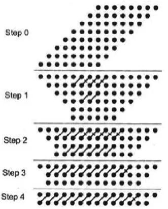
V. DADDATREE MULTIPLIER STRUCTURE
Dadda refined Wallace‘s method by defining a counter placement strategy that required fewer counters in the partial product reduction stage at the cost of a larger carry propagate adder. This method has three major steps.
Step1: Multiply each bit of one of the arguments, by each bit of the other, yielding N2 results.
[image:4.595.74.273.478.672.2]International Journal of Emerging Technology and Advanced Engineering
Website: www.ijetae.com (ISSN 2250-2459, ISO 9001:2008 Certified Journal, Volume 5, Issue 9, September 2015)
305
a)Let d1 = 2 and di+1 = [3.di / 2], where di is the matrix height for the ith stage from the end. Find the largest i such that at least one column of the matrix has more than di bits.
b) By using (2, 2) and (3, 2) counters to obtain a reduced matrix, with no more than di elements in any column.
c) Let i = i-1 and repeat step b, until a matrix with only two rows is generated.
Step 3: Group the wires in two numbers and add them with conventional adder.
[image:5.595.86.252.350.556.2]Dadda has introduced a number of ways to compress the partial product bits using such a counter which is known as Dadda‘s counter. Figure 5 gives the process for 8x8 bits Dadda multiplier.
Figure 5. 8 X 8 Dadda Tree multiplier structure
VI.SIMULATION RESULTS
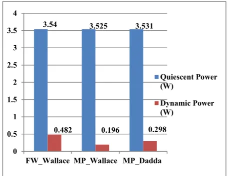
[image:5.595.306.545.370.449.2]The programming has been done in Verilog HDL and it is simulated using Xilinx ISE Tools and ISim simulator. Power analysis is done by using XPower Analyzer. The simulation results of 32 bit and 64 bit reconfigurable multipliers which are implemented in Wallace and Dadda Tree structures are shown in Figure 6 and Figure 7 respectively. The power report of 32 bit MP multiplier by Wallace & Dadda Tree, which is analysed by XPower Analyzer is shown in Figure 8 and Figure 9 respectively while the power analysis of 32 bit and 64 bit multipliers with different multiplication methods are shown in Figure 10 and Figure 11 respectively. The area, delay and power comparisons of different multipliers are presented in Table I and Table II. Comparison of 7 tap FIR filters which are implemented by fixed width multiplier (Wallace Tree) and reconfigurable MP multipliers (Wallace and Dadda Tree) are presented in Table III.
[image:5.595.308.543.477.557.2]Figure 6. Simulation results of 32 X 32 bit MP multiplier by Wallace Tree
Figure 7. Simulation results of 64 X 64 bit MP multiplier by Dadda Tree
[image:5.595.87.523.618.755.2]International Journal of Emerging Technology and Advanced Engineering
Website: www.ijetae.com (ISSN 2250-2459, ISO 9001:2008 Certified Journal, Volume 5, Issue 9, September 2015)
[image:6.595.89.518.161.283.2]306
Figure 9. Power report of 32 Bit MP multiplier by Dadda Tree
TABLE I.AREA,DELAY AND POWER COMPARISONS OF 32BIT MULTIPLIERS
Multiplication Methods
Area Delay (nS)
Power (W) LUT Slices
32 bit Fixed Width(FW) multiplier (Wallace Tree
structure)
2070 827 28.838 4.023
32 bit 3 sub block MP Multiplier (Wallace Tree
structure)
1744 750 36.116 3.722
32 bit 3 sub block MP Multiplier (Dadda Tree
Structure)
1945 829 31.358 3.829
TABLE II. AREA,DELAY AND POWER COMPARISONS OF 64BIT MULTIPLIERS
Multiplication Methods
Area Delay
(nS) Power (W) LUT Slices
64 bit 3 sub block MP Multiplier (Wallace
Tree)
5408 2409 67.509 3.881
64 bit 3 sub block MP Multiplier (DaddaTree)
[image:6.595.311.540.316.493.2]7147 2741 44.482 3.927
[image:6.595.57.285.334.558.2]Figure 10. Power Analysis of 32 Bit Multiplication with Different Design Methods
Figure 11. Power Analysis of 64 Bit Multiplication with Different Design Methods
3.54 3.525 3.531
0.482 0.196 0.298
0 0.5 1 1.5 2 2.5 3 3.5 4
FW_Wallace MP_Wallace MP_Dadda
Quiescent Power (W)
Dynamic Power (W)
3.54 3.54
0.348 0.391
0 0.5 1 1.5 2 2.5 3 3.5 4
MP_Wallace MP_Dadda
Quiescent Power (W)
[image:6.595.317.540.536.698.2]International Journal of Emerging Technology and Advanced Engineering
Website: www.ijetae.com (ISSN 2250-2459, ISO 9001:2008 Certified Journal, Volume 5, Issue 9, September 2015)
[image:7.595.55.286.161.366.2]307
Table III. Comparison of 7 TAP FIR Filter by Using Different MultipliersFIR implementation by
Different multipliers LUT Delay (nS)
FIR by fixed width
multiplier(Wallace Tree) 105830 25.339
FIR by MP multiplier
(Wallace Tree) 92317 37.915
FIR by MP Multiplier
(Dadda Tree) 103562 26.510
VII. CONCLUSION
The proposed novel MP multiplier which is implemented by Dadda Tree, featuring with variable precision and parallel processing provides up to 64 X 64 bit multiplication. 32 X 32 bit MP multiplier by Wallace Tree has better optimization in terms of area and power when compared to fixed width multiplier by Wallace Tree as well as MP multiplier by Dadda Tree. But the MP Dadda multiplier has better optimization in Delay compared to the other multipliers. The proposed 32 bit MP multiplier by Dadda Tree structure is achieving 13.17% of delay reduction compared to the MP multiplier by Wallace Tree and obtaining 4.82% of power reduction compared to the Fixed Width Multiplier. Hence it is a better trade-off for compromising the power, delay and area compared to fixed width and MP multiplier by Wallace Tree. A DSP application such as FIR filter is implemented using different multiplication methods and Dadda multiplication technique had obtained a better delay in various DSP applications and Delay in FIR Filter is compared.
REFERENCES
[1] T. Kuroda, ―Low power CMOS digital design for multimedia
processors,‖ in Proc. Int. Conf. VLSI CAD, Oct. 1999, pp. 359–367.
[2] A. Wang and A. Chandrakasan, ―Energy-aware architectures for a
realvalued FFT implementation,‖ in Proc. IEEE Int. Symp. Low
Power Electron. Design, Aug. 2003, pp. 360–365.
[3] K.-S. Chong, B.-H. Gwee, and J. S. Chang, ―A micropower
low-voltage multiplier with reduced spurious switching,‖ IEEE Trans. Very Large Scale Integr. (VLSI) Syst., vol. 13, no. 2, pp. 255–265, Feb. 2005.
[4] S.-R. Kuang and J.-P. Wang, ―Design of power-efficient
configurable booth multiplier,‖ IEEE Trans. Circuits Syst. I, Reg. Papers, vol. 57, no. 3, pp. 568–580, Mar. 2010.
[5] M. Sjalander, M. Drazdziulis, P. Larsson-Edefors, and H.
riksson,―A low-leakage twin-precision multiplier using
reconfigurable power gating,‖ in Proc. IEEE Int. Symp. Circuits Syst., May 2005, pp. 1654–1657.
[6] S.-R. Kuang and J.-P. Wang, ―Design of power-efficient pipelined
truncated multipliers with various output precision,‖ IET Comput. Digital Tech., vol. 1, no. 2, pp. 129–136, Mar. 2007.
[7] H. Lee, ―A power-aware scalable pipelined booth
multiplier,‖in Proc. IEEE Int. SOC Conf., Sep. 2004, pp. 123–126.
[8] A. Bermak, D. Martinez, and J.-L. Noullet, ―High-density
16/8/4-bit configurable multiplier,‖ Proc. Inst. Electr. Eng. Circuits Devices Syst., vol. 144, no. 5, pp. 272–276, Oct. 1997.
[9] G. Y. Jeong, J. S. Park, and H. C. Kang, ―A Study on multiplier architecture optimized for 32-bit processor with 3-stage pipeline,‖ in Proc. Int. SoC Design Conf., Oct. 2004, pp. 656–660.
[10] J.-Y. Kang and J.-L. Gaudiot, ―A simple high-speed multiplier
design computers,‖ IEEE Trans. Comput., vol. 55, no. 10, pp. 1253–1258, Oct. 2006.
[11] ShahzadAsif and Yinan Kong ―Low-Area Wallace Multiplier‖
Hindawi Publishing Corporation VLSI DesignVolume 2014, Article ID 343960.
[12] R. Min, M. Bhardwaj, S.-H. Cho, N. Ickes, E. Shih, A. Sinha, A.
Wang, and A. Chandrakasan, ―Energy-centric enabling
technologies for wireless sensor networks,‖ IEEE Wirel. Commun.,
vol. 9, no. 4, pp. 28–39 ,Aug. 2002.
[13] M. Bhardwaj, R. Min, and A. Chandrakasan, ―Quantifying and
enhancing power awareness of VLSI systems,‖ IEEE Trans. Very
Large ScaleIntegr. (VLSI) Syst., vol. 9, no. 6, pp. 757–772, Dec. 2001.
[14] S. D. Haynes, A. Ferrari, and P. Y. K. Cheung, ―Flexible
reconfigurable multiplier blocks suitable for enhancing the architecture of FPGAs,‖ in Proc. IEEE Custom Integr. Circuits, May 1999, pp. 191–194.
[15] XiaoxiaoZhangand and FaridBoussaid, ―32 Bit×32 Bit
Multiprecision Razor-Based DynamicVoltage Scaling Multiplier with Operands Scheduler,‖ IEEE Trans. On very large scale integration Systems, Vol 22, No4, April 2014.
Mrs. K.TANUJA received B.Tech degree in Electronics and Communication Engineering from JNTUK and presently pursuing M.Tech degree in VLSI in MVGR College of Engineering,
Vizianagaram. My research interests include
VLSI Design, Low Power VLSI and DSP Architectures.