International Journal of Emerging Technology and Advanced Engineering
Website: www.ijetae.com (ISSN 2250-2459, ISO 9001:2008 Certified Journal, Volume 4, Issue 7, July 2014)
461
Implementation Methodology of High Performance Multi Byte
Data Access Control of AMBA Bus
A. Anendhar
1, C. Srilatha
21Assistant Professor, 2Professor, Department of Electronics and Communication Engineering, Aurora’s Scientific Technological
and Research Academy, Bandlaguda; Hyderabad (Dt); A.P, India.
Abstract-- Earlier the memories used to have more speed than the processors. But with the invention of Microprocessors and Microcontroller the speed of the memory has become lesser than these processors. So with the improvement of Microprocessor these years, the memory access time has been a bottleneck which limits the system performance. Even though the system has high frequency every application needs to access the memory several times and the memories have lesser speed than the processor. So the memory accessing time definitely limits the system performance. This paper describes an approach to increase the system performance by using on-chip bus i.e. Advanced microcontroller Bus Architecture (AMBA) AHB bus with Burst operation, in the burst operation the data will be transferred from/to the sequential locations of the memory. Each transfer has definite time. This architecture may reduce the memory latencies and bandwidths. The result is that the memory accessing time will be reduced, which increases the system performance.
Keywords-- ARM; AMBA; AHB; APB; Memory controller.
I. INTRODUCTION
The AMBA is developed by the ARM integrated laboratories. The AMBA is a system on chip bus; it provides two buses like AHB and APB. The AHB is a high speed bus used for high speed devices where as APB is a low speed bus used for low performance peripherals [1].
With the increasing the system frequency, it’s hard to complete the address decoding and memory access operations in one clock cycle. Therefore, wait states are inserted into the data cycle to ensure there is enough time for address decoding and memory accessing. But with method that inserting wait state will cause system performance drop dramatically. Another approach to increase the system performance by using existing AMBA AHB bus with burst operation. The processor with a high speed is synchronized with low speed memory by using a asynchronous FIFO, the FIFO which uses the pointers of gray code representation. The system which does the above work is called Memory Controller [6]. The Memory Controller designed so that it should verify all the possible multi byte data transfer with 4-beat, 8-beat, and 16-beat burst operation.
II. PREVIOUS WORK
Earlier many methods have proposed to increase the system performance like one method proposed with an AMBA AHB and APB bridge in which handshaking signal have used to synchronize the low performance peripheral with high performance processor[3]. But with the use of handshaking signals the complexity of the system increases. The second method proposed with an AMBA AHB burst operation. In which only 4-beat burst operation used to reduce the memory latency. The minimum period used in the above design is 57.142ns and maximum frequency is 17.500MHz [2].
III. APPROACH
The architecture uses only one master and only one slave and do not require the use arbitration scheme. As the bus is free to the master every time the master sends the block of information in the following manner.
Firstly the master asserts the HCLK signal with a frequency of specified value, as the address present in the HADDR [31:0] the slave of the specified location will be selected. The slave asserts the control signals like HREADY whenever it is ready to accept the data. The slave uses a low speed clock MCLK which has normally frequency less than the master clock frequency, so the synchronization between the low performance peripheral and high speed master can be achieved by Asynchronous FIFO. The depth of the FIFO depends on the value of burst size. The burst operation is the process of splitting the data into many bytes and transferring the same data into sequential memory locations.
International Journal of Emerging Technology and Advanced Engineering
Website: www.ijetae.com (ISSN 2250-2459, ISO 9001:2008 Certified Journal, Volume 4, Issue 7, July 2014)
462
The burst operation here used is normally an 8-beat burst or 16-beat burst then the total no of bytes transferred into sequential locations in each type transfer is (size × beats) 32 bytes or 64 bytes respectively [4].IV. TOOLS
This architecture is synthesized with Xilinx ISE software tool produced by Xilinx for synthesis and analysis of HDL designs [8].
The target device used for the design of this architecture is Spartan-3E family. These Spartan-3E FPGA enhancements, it is mixed with advanced 90 nm process technology, generates more functionality and bandwidth per dollar than was previously possible, arranging new standards in the programmable logic industry.
The architecture programming done in Verilog HDL [9].
Product Name Value
Family Spartan 3E
Device XC3S1200E
Package FG400
Speed -4
Top–Level Source Type HDL
Synthesis Tool XST(VHDL/Verilog)
Preferred Language Verilog
Implementation:
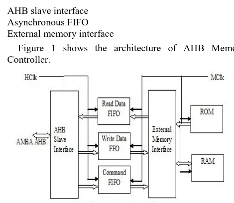
The Architecture for implementing BURST transfer with AMBA AHB bus consists of three modules:
1. AHB slave interface 2. Asynchronous FIFO 3. External memory interface
Figure 1 shows the architecture of AHB Memory Controller.
Figure1. Architecture of AHB Memory Controller
AHB Slave Interface:
The AHB Slave interface generates the Addresses with HBurst signal; the possibilities with HBurst Signal are given in Table 1[4].
TABLE 1. HBurst Encoding
HBURST[2:0] Type Description
000 Single Single Transfer
001 Inc Inc burst of length 6
010 Wrap4 4-beat wrap burst
011 Incr4 4-beat inc burst
100 Wrap8 8-beat wrap burst
101 Incr8 8-beat inc burst
110 Wrap16 16-beat wrap burst
111 Incr16 16-beat inc burst
[image:2.612.336.551.455.563.2]The size of the data can be selected by the following table with Hsize signal [4]
TABLE 2. Hsize encoding
HSIZE[2:0] Size Description
000 8 bits Byte
001 16 bits Half word
010 32 bits Word
[image:2.612.41.276.491.695.2]International Journal of Emerging Technology and Advanced Engineering
Website: www.ijetae.com (ISSN 2250-2459, ISO 9001:2008 Certified Journal, Volume 4, Issue 7, July 2014)
463
Figur2. Burst operation state machine
Asynchronous FIFO:
Asynchronous FIFO’s are used to synchronize the high speed master with low speed peripherals. Asynchronous FIFO used here is the depth of 256 locations; each of the location is about 32 bits. The pointer used for address for pointing the write pointer and read pointer is a gray code pointer [5].
Write Operation:
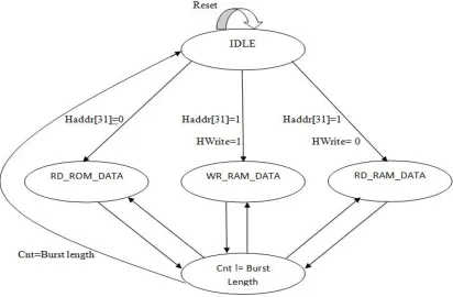
AHB Master will be in IDLE state at the initial stage, based on the HWRITE signal the AHB Master either goes to WRITE or READ state. If HWRITE signal is HIGH it indication of write transfer operation i.e. the data is transferred from master to slave. When AHB master go WRITE state and will issue address (HAddr) and data will be written into the FIFO with sequential addressing. The depth of the FIFO depends on the value of burst size. The write operation in FIFO explained as follows.
The Asynchronous FIFO is a First-In-First-Out memory unit with queuing control logic that function as a controller for read and write pointers, generation of status flags, and necessary handshake signals for connecting with the user logic.
FIFO status cannot be contaminated by false requests. Accessing a read operation even though the EMPTY flag is active will not affect the current status of the FIFO. Similarly, accessing a write operation even though the FULL flag is active will not affect the current state of the FIFO. If enabled, the RD_ERR and WR_ERR status signals will indicate the removing of these false requests.
In this input data is giving from the HCLK and the output data is taking from the MCLK, here the read and write operations are inputs to the WRITE FIFO. Here the data is stored in the write FIFO up to the 256 bits after filling the 256 bits the FIFO shows FIFO is FULL signal.
Figure3. FIFO Write operation
The write pointer always points to the next word to be written; therefore, on reset, both pointers are set to zero, which also happens to be the next FIFO word location to be written. On a FIFO-write operation, the memory location which is pointed by the write pointer is written, then the pointer is incremented by one to points the next location to be written. Similarly, the read pointer always points to the current FIFO word to be read. Once the first data word is written to the FIFO, the write pointer incremented by one memory location, the empty flag is cleared, and the read pointer that is still pointing to the data which is in the first memory word, immediately drives that first valid word onto the FIFO data output port, to be read by Memory[5].
Read Operation:
If HWRITE signal is LOW it indication of write transfer operation i.e. the data is transferred from slave to the master. In the READ state the Master will give address (HAddr) and make HWrite signal to low. The data in the given address will be read and written into the FIFO. In this input data is giving from the MCLK and the output data is taking from the HCLK, here the read and write operations are the inputs to the READ FIFO. Here the stored data can be retrieved by the data out when the FIFO is EMPTY the EMPTY flag is activated.
International Journal of Emerging Technology and Advanced Engineering
Website: www.ijetae.com (ISSN 2250-2459, ISO 9001:2008 Certified Journal, Volume 4, Issue 7, July 2014)
464
Once the first data is written into the READ FIFO by the Mclk the write pointer increments, and the data is read by the master through the Data out signal.In the above procedure the data will be sychronized with the Asynchronous FIFO in BURST operation. By the methodology of split transactions the data speed can be increased[10].
Status of the FIFO:
The status condition of the FIFO can be known by the Status bit, if it is SET and read and write pointers are having equal address then the FIFO is FULL. If the Status bit is RESET and write and read pointer address are equal then the FIFO is EMPTY. The status signal is implemented by the circuit is shown in the figure 5[5]
Figure5. Status of the FIFO.
External Memory Interface:
The external memory interface identifies the address location of the data based on the address signal and also controls the cycle timings of read and write operation[4]. The state machine for external memory is shown in the figure 6.
Figure6.External memory interface state machine
Memory Mapping:
[image:4.612.64.270.569.704.2]The memory mapping is a part of the external memory interface to select the memory bank from RAM and ROM. The memory controller has four banks, which are selected by the MCSN signal [4].The memory mapping is shown in the Table 3.
TABLE 3. MCSN Encoding
HSelect HAddr[31] HAddr[1:0] MCSN
0 X XX 0000
1 0 00 0001
1 0 01 0011
1 0 10 0111
1 0 11 1111
1 1 00 0001
1 1 01 0011
1 1 10 0111
1 1 11 1111
The arm processor is a 32 bit RISC processor it can addressable up to 232 locations, each of which is byte width. However these memory locations are selected by the MCSN signal. The memory system architecture is shown in the figure 7. In which the lowest two address bits are used for selecting Memory banks of the ROM and SRAM [4].
Figure7. Memory system architecture
V. TESTING AND SIMULATION RESULTS
International Journal of Emerging Technology and Advanced Engineering
Website: www.ijetae.com (ISSN 2250-2459, ISO 9001:2008 Certified Journal, Volume 4, Issue 7, July 2014)
465
Result Analysis:
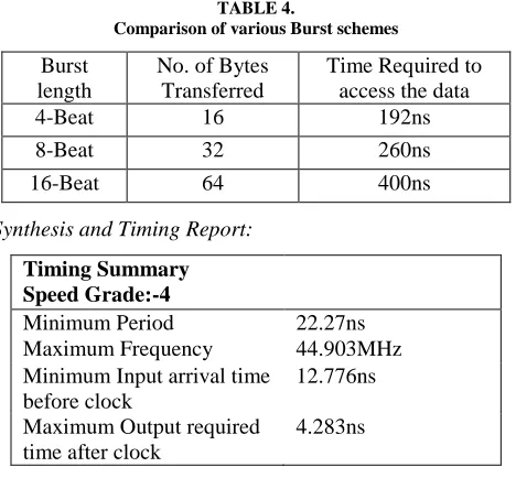
[image:5.612.52.286.180.397.2]The comparison of various burst schemes and its timing access values are given in table 4.
TABLE 4.
Comparison of various Burst schemes
Burst length
No. of Bytes Transferred
Time Required to access the data
4-Beat 16 192ns
8-Beat 32 260ns
16-Beat 64 400ns
Synthesis and Timing Report:
Timing Summary Speed Grade:-4
Minimum Period 22.27ns
Maximum Frequency 44.903MHz Minimum Input arrival time
before clock
12.776ns
Maximum Output required time after clock
4.283ns
VI. CONCLUSION
The time required to access the multiple bytes has been decreased successfully by the use of burst operation. Incrementing bursts access sequential locations and the address of each transfer in the burst is just an increment of the previous address.
Burst operation has performance benefits because when the first beat of a burst is accepted, it contains data about the remaining beats. For example, from the first beat of a read burst, all the data required to complete the transfer can be read from memory. This first transfer has some delay before data is returned. Subsequent beats of the burst can have less delay because the data they require might have already been read from the memory. From the AHB Memory controller we conclude that minimum period used in the design is 22.27ns and maximum frequency is 44.903MHz which is comparatively good result.
REFERENCES
[1] Rishabh Singh Kurmi, Shruthi Bhargava “Implementation of an
AMBA Advanced High performance Bus Protocol IP Block” IJECCE, June2011,Vol.1,Issue 1,no.2.
[2] Rishabh Singh Kurmi, Shruthi Bhargava “The design of AHB
Protocol Block for Advanced Microcontrollers” IJECa, October 2011,Vol.32,Issue 1,no.8.
[3] Vani.R.M and M.Roopa “Design of AMBA Based AHB2APB
Bridge” IJCSNS, Novenber 2010, Vol.10,Issue 1,no.11.
[4] “AMBA Specification (Rev2.0)”, ARM Inc.
[5] “Simulation and Synthesis Techniques for Asynchronous FIFO
Design with Asynchronous Pointer Comparisons” Clifford E. Cummings Sunburst Design, Inc.
[6] “Prime Cell AHB SRAM/NOR Memory Controller”, Technical
Reference Manual, ARMInc.
[7] “AHB Example AMBA System”, Technical Reference Manual,
ARM Inc.
[8] www.xilinx.com