International Journal of Emerging Technology and Advanced Engineering
Website: www.ijetae.com (ISSN 2250-2459,ISO 9001:2008 Certified Journal, Volume 4, Issue 8, August 2014)
375
HVDC Transmission Using Capacitors
Gurrala Nagaraju
1, G. Jaya Prakash
2, S. John Powl
3Sri Manakula Vinayagar Engineering College, Pondicherry
Abstract--This paper proposed a single-phase single-stage high DC voltage using capacitor instead of power transformer and converter circuits. The conversion of high DC voltage converter without a transformer is involved. AC input is controlled by IGBT switch which the current flow in both directions of the capacitor. Simulation results are provided to show the effectives of the proposed technique. This paper presents how capacitor is used in HVDC links.
Keywords-- [Capacitor, Voltage multiplier, switched capacitor, HVDC link, Matlab]
I. INTRODUCTION
HVDC system was used for transmission of electrical power to large distance. In generating stations they generate 11KV AC [ 1]. This 11KV AC was given to a power transformer for step up the voltage into 500KV AC. By using converter 500KV AC is converted to 500KV DC. Then 500KV DC was transmitted to long transmission line.
Similarly in the receiving end the 500KV DC was converted into 500KV AC by using inverter and step down to 110KV by using power transformer. After that the stepped down voltage was sent to the distribution system[2].
By using power transformer some losses have been occurred such as core loss, copper loss, and loss due to insulation medium etc. so minimum 20% of generated power becomes waste during transmission. Along with this, they also need frequent maintenance.
The transmission loss was reduced and more stable system was obtained in case of HVDC transmission. The step up and step down action was done by different voltage conversion techniques. The main advantage of the system is it can perform the action of both step up and AC to DC conversion. Hence the converter was absent in modified voltage multiplier system. The model was analyzed by using MATLAB software.
[image:1.595.313.550.308.413.2]Existing HVDC System
Figure 1
The above diagram shows the present HVDC system. Initially the generated voltage was giving to the power transformer for step up the 11KV AC to 500KV AC [3]. Later it was converted to DC by using converter circuit.
The electric power was transmitted to long distance and at receiving end it was converted to AC by using inverter and step down to 110KV AC by power transformer.
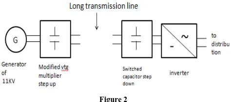
Proposed HVDC System
Figure 2
The above figure shows the proposed HVDC system. In this system the source from the generating station (11KV) is directly sent to modified voltage multiplier. The modified voltage multiplier is stepped up 11KV AC source into 550KV and at the same time it converts it into DC source [4]. After stepped up the DC source is transmitted to transmission system for long transmission.
In the receiving end 550KV DC is stepped down into 137KV DC using switched capacitor method. Using inverter DC source 137KV is converted into AC source. Then it is sent to distribution system. In the proposed HVDC system there is an absent of power transformer and converter. The rating of the inverter is also reduced[1,5].
Voltage Conversion Technique
Power transformer was removed from existing HVDC system by different voltage conversion techniques for step up and step down of voltage. Step up and step down actions are takes place by series and parallel action of capacitor [6]. The different voltage conversion techniques are:
Switched capacitor circuit.
Voltage multiplier circuit.
International Journal of Emerging Technology and Advanced Engineering
Website: www.ijetae.com (ISSN 2250-2459,ISO 9001:2008 Certified Journal, Volume 4, Issue 8, August 2014)
376
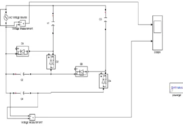
II. SWITCHED CAPACITOR CIRCUIT [image:2.595.56.266.152.318.2]Step Up
Figure 3
The above figure shown is single stage switched capacitor circuit diagram. Initially positive gate pulse was given to IGBT and IGBT1 which results in conduction. Hence two capacitors are connected in parallel with the source voltage. Then negative pulse was given to those IGBT to turn it OFF. At the same time positive pulse was given to IGBT2 and IGBT4 to turn it ON[7]. Hence both the capacitor became series to the load. The operation of the circuit was shown below.
Initially the both the capacitors are charged to a voltage of ‘V’ due to parallel connection with voltage source. In the next stage both the capacitors are connected in series and connected in parallel with the load. Now the voltage across load is ‘2V’. Hence the input voltage ‘V’ was stepped up to a voltage ‘2V’.
In this method large power cannot be transfer because it needs very high capacitance value. Voltage oscillation was large for a small load of few kilo watts [8]. So instead of that voltage multiplier was analyzed.
Step Down
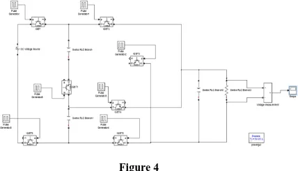
Figure 4
In the above figure initially both the capacitors are connected in series with the voltage source. Hence both the capacitor is charged to half of the input voltage. Then it was connected in parallel to the load for discharge.
The voltage fluctuation was mainly depending on two factors such as capacitance of the capacitor and switching time of the capacitor.
Drawback
Switched capacitor method involves in lot of switching actions. Hence it requires pulse transformer. IGBT cost was very high because of high power rating. Due to lot of switching action harmonics also produce. Generating alternating current should be converted into direct current using converter, then by using switched capacitor method the voltage can be step up. By this method the converter rating was reduced, but there is no need of converter in voltage multiplier method and modified voltage multiplier method.
III. VOLTAGE MULTIPLIER METHOD
Voltage multiplier method was another method to step up the input DC voltage. Its circuit contains only capacitors and diodes for step up. The alternating voltage source itself makes the diode to conduct certain period of time and remain in OFF position for some period because of its alternating nature.
Figure 5
The above shown diagram was the single stage voltage multiplier circuit. This circuit was used to step up the input AC voltage [9]. It also convert the input AC voltage into the stepped up DC voltage so there is no need of converter. So the converter cost was reduced.
During Positive Cycle Of Source
Initially the diode gets forward biased in the positive half cycle. Due to forward bias when the input voltage increases above the forward breakdown voltage diode gets turned ON[2,10]. Hence the capacitors get charged to the peak input voltage.
[image:2.595.66.280.589.712.2]International Journal of Emerging Technology and Advanced Engineering
Website: www.ijetae.com (ISSN 2250-2459,ISO 9001:2008 Certified Journal, Volume 4, Issue 8, August 2014)
377
During Negative Cycle Of Source
In the next half cycle diode1 get forward biased and diode was reverse biased. Hence the charged capacitor and voltage sources become parallel in series with capacitor1. Capacitor1 was charged to voltage of 2V. This cycle was goes on repeating to transfer the electrical power.
The above figure represents as voltage multiplier one stage circuit. By cascading n-number voltage can be stepped up to the desired value. For each stage the voltage build was 2V i.e. twice of the input voltage
[image:3.595.376.480.155.305.2]Voltage Multiplier Circuit Of 10 Stages
Figure 6
The above figure is 10 stages voltage multiplier circuit. During the positive half cycle top capacitors are get charged due to conduction of forward biased diodes. During the other half cycle capacitors located at the bottom are charged. For 12 stages the voltage stepped up was 20*V for input AC voltage(V).
The output for 28 stages was shown in below graph. In the graph time was taken as x-axis and voltage in y-axis. From the graph it was observed that is the not constant with respect to the time. A load of 100KW was applied to the circuit. So this type of circuit was not suitable for the transfer of large power even though it transfer more power compare to switched capacitor.
Modified Voltage Multiplier (Two Stage)
The below shown figure was two stage modified voltage multiplier. The input AC voltage has frequency of 50HZ. Hence it takes 20ms per cycle. For positive half cycle it takes 10ms and for negative half cycle it takes another 10ms.
In first half cycle diode D1 is conducted so capacitor C1 is charged at voltage of input voltage source i.e. V
.
Figure 7
MODE-I
Figure 8
In the negative half cycle diode D2 get conducted which result in voltage source and capacitor C1 gets series and become parallel with capacitor C2. Hence capacitor C2 charged to a voltage of 2V.
MODE-II
[image:3.595.358.499.439.610.2]In the next positive half cycle diode D1 and D3 is forward bias and starts conducting hence voltage source and capacitor C2 becomes series in parallel with capacitor C3. So capacitor C3 charged to a voltage of 3V
[image:3.595.72.255.622.754.2]International Journal of Emerging Technology and Advanced Engineering
Website: www.ijetae.com (ISSN 2250-2459,ISO 9001:2008 Certified Journal, Volume 4, Issue 8, August 2014)
378
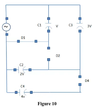
[image:4.595.312.554.140.294.2]MODE-III
Figure 10
During next negative cycle diode D2&D4 is forward bias and diode D1&D3 is reverse bias. So D2&D4 is turn ON and the capacitor C3 and source voltage is series in parallel with capacitor C4. The charge stored in the capacitor C4 has 4V.
MODE-IV
[image:4.595.85.243.150.333.2]In sub system 1 contains 25 stages for stepped up. During positive half cycle odd number diodes are forward bias and even number capacitors are charged.
Figure 11
During negative half cycle odd number diodes get reverse bias which results to turn ON. So the even number capacitors are charged. Similarly this cycle charging and discharging goes on repeating. In capacitor C50 charge to a voltage of 50V if a voltage of 11KV was given as input. The voltage obtained from C50 was 550KV.
Output For Proposed Model
Figure 12
The above diagram was the output of our proposed model. We have given an input of 11KV AC supply. The modified voltage multiplier circuit step up 11 KV AC voltage into 40KV and at the same time it acts like an converter by converting the AC voltage into DC voltage.
The main advantage of this modified voltage multiplier is we can replace the transformer and converter by a single circuit.
Capacitor Design
The capacitor value has to be designed depend up on the power that has to be transmitted. It also depends upon the switching time of source. In this paper capacitance value of capacitor was designed using transfer function.
IV. CONCLUSION
Switched capacitor method involves in more number of switching action and a separate pulse generator was needed. Switched capacitor method need converter at the input side which increases the initial installation cost. So we are going for other voltage conversion technique known as voltage multiplier.
Voltage multiplier method cannot transfer large power because many capacitors are only used for voltage division not for transfer of power, because only first and last capacitor terminal connected to the load and source. So to get more efficient power transfer modified voltage multiplier circuit was used to step up the input voltage and also convert the input AC to DC voltage.
International Journal of Emerging Technology and Advanced Engineering
Website: www.ijetae.com (ISSN 2250-2459,ISO 9001:2008 Certified Journal, Volume 4, Issue 8, August 2014)
379
REFERENCE[1] Rahim N.A And Omar A.M; "Three-phase Single-Stage High-Voltage DC Converter", IEE Proceedings Generation, Transmission and Distribution, vol. 149, Issue: 5, Sept. 2002, pp. 505 - 509
[2] Wang, J., Dunford, W., and Mauch, K., "A Comparison Between Some Proposed Boost Topologies and Conventional Topologies InDiscontinuous Inductor Current Mode", Proceeding of 22nd annual IEEE international Conference on Industrial Electronic, control and instrumentation (IECON) 1996, Vol. 3, pp. 1524 - 1529 [3] Lopez, O., Garcia De Vicuna, L., Matas, J., Castilla, M., and Lopez, M.: "A New Family of Single-Stage High Power-Factor AC/DC Converters", Proceeding of 31St annual IEEE Power Electronic Specialist Conference. (PESC) 2000, Vol. 3, pp. 1445 - 1450
[4] Lu, Z., Chen. H., Qian, Z., and Green, T.C.: "An Improved Topology of Boost Converter with Ripple-Free Input Current", Proceedings of 15th annual IEEE Applied Power Electronics Conference and Exposition, (APEC) 2000, Vol. 1, pp. 528 – 532
[5] Iqbal, S.; "A three-phase Symmetrical Multistage Voltage Multiplier", IEEE Power Electronics Letters, vol. 3, Issue 1, March 2005, pp. 30 - 33
[6] Bellar, M.D.; Watanabe, E.H.; Mesquita, A.C.; "Analysis of the Dynamic and Steady-state performance of Cockcroft-Walton Cascade Rectifiers", IEEE Transactions on Power Electronics, vol. 7, Issue 3, July 1992, pp. 526 - 534
[7] Wismer, M.G.; "Steady-state Operation of a High-voltage Multiresonant Converter in a High-Temperature Environment", IEEE Transactions on Power Electronics, vol. 18, Issue 3, May 2003, pp. 740 - 748
[8] Holtz, J.; "Pulsewidth modulation for electronic power conversion", Proceedings of the IEEE, vol. 82, Issue 8, Aug. 1994, pp. 1194 - 1214
[9] The Programmable Logic Data Book, Xilinx Databook, 1998 [10] C.T.Baldwin M.A. M.I.E.E.'Fundamentals of Electrical
Measurement', Harrap, London, 1961