© 2015, IRJET.NET- All Rights Reserved
Page 190
Test variables selection and multiple parametric faults detection in
nonlinear analog circuits
G.Puvaneswari
1, S.UmaMaheswari
21
Asst. Prof. (SG), Department of Electronics and Communication Engineering, Coimbatore Institute of Technology,
Coimbatore-641 014, Tamil Nadu, India.
2
Associate Professor,
Department of Electronics and Communication Engineering, Coimbatore Institute of
Technology, Coimbatore-641 014, Tamil Nadu, India.
---***---Abstract -
A method to select diagnosis variables ortest variables for analog circuit testing and to diagnose multiple soft faults in non linear analog circuits using multiple frequency measurements is proposed in this paper. Circuit parameters or the test variables are derived by simulating the circuit under test (CUT) using Modified nodal analysis (MNA) method and are selected based on test vectors. Test vectors associated with each component of CUT are generated with the knowledge of circuit topology and the component values. Testing is performed at multiple frequency measurements to solve the component tolerance challenge in analog circuit testing. The results obtained from simulation of benchmark circuits show the effectiveness of the proposed approach
Key Words:
analog circuit – fault diagnosis – test
vector –tolerance –test variable – multiple frequency-
modified nodal analysis
1. INTRODUCTION
Analog circuit testing is an important research topic because of non availability of standard procedures or models. The research challenges such as component tolerance, diagnosis variables or test variables, number of diagnosis variables, suitable test frequencies and test nodes selection in analog circuit testing limit the development of standardized approaches for testing. Analog circuit faults are classified as hard faults or catastrophic faults and soft faults or parametric faults. Parametric faults are defined as the variation in component values and hard faults are open or short circuits. Most of the research proposals are for parametric
faults detection because parametric faults lead to system performance degradation and are hard to detect. A method based on thresholding approach to detect multiple parametric faults in linear analog circuits is proposed by G.Puvaneswari in [1]. Jian Sun proposed principal component analysis (PCA) and particle swarm optimization (PSO) support vector machine (SVM) based analog circuit fault diagnosis method [2]. To reduce the fault feature dimension principal component analysis and data normalization is used as preprocessing and support vector machine method is used to diagnosis, and particle swarm optimization is used to optimize the penalty parameters and the kernel parameters of SVM, that improve the recognition rate of the fault diagnosis. A slope fault model based fault dictionary approach is proposed by Yang in [3] to select test points and diagnose parametric and hard faults. In [4], Long B introduced a near-optimal feature vector selection method based on Mahalanobis distance for diagnosis of analog circuits using the least squares SVM (LS-SVM). In [1], G.Puaneswari proposed a test vector based multiple fault diagnosis of linear analog circuits. Multiple faults are identified based on the threshold estimated from the fault variables derived for the components of the CUT. A component is said to be faulty if the fault variable is less than the threshold. This paper uses the threshold approach proposed in [1] to detect multiple parametric faults in nonlinear analog circuits and to solve tolerance issue in testing; testing is done at multiple frequency measurements. Test variables selection is done through the test vector values.
© 2015, IRJET.NET- All Rights Reserved
Page 191
proposed approach with simulation results on bench markcircuits and discuss the results. Section 5 concludes.
2. MATHEMATICAL BACKGROUND
Testing of analog circuits begins with the simulation of the CUT and deriving the diagnosis variables such as node voltages and branch currents. The simulation of an electronic circuit involves formulation of the circuit equation and solving it for the unknowns. To simulate the CUT, Modified Nodal Analysis (MNA) is used as explained by C.-W.Ho & Jiri Vilach in [5] & [6]. MNA for linear systems results in the system equation of the form
AX
Z
(1)where A is the coefficient matrix, X is the unknown vector consists of circuit variables (node voltages and few branch currents) and Z is the excitation matrix. The circuit coefficient matrix is formed by the sub matrices,
A
=
D
C
B
G
(2)
G
is the conductance of the components in the CUT and the values ofG
are determined by the interconnections of the circuit components.B
andC
matrices consist of 0, 1,-1 and the values are based on the interconnections of the voltage sources. TheD
matrix is developed with zeros for independent sources and has nonzero values for dependent sources. X is the unknown vector consists of circuit variables (node voltages and few branch currents which are useful for testing and Z is the excitation matrix. The right hand side matrix (Z) consists of the values of independent current and voltage sources. The unknown vector is found by matrix inverse operation.
v n
I
V
X
(3)
V
I
Z
(4)In case of non linear circuits, the nonlinear devices are replaced by its linearized complete small signal model as explained by Adel S. Sedra in [8]. Non linear device terminal currents are introduced as unknown currents in addition to other circuit parameters. As the non linear
devices are dependent sources D matrix consists of values corresponding to the device parameters. Faults in the CUT are simulated using Fault Rubber Stamp (FRS) as explained by Jose A. Soares Augusto in [7]. FRS is based on the MNA stamp of the components of a CUT. The MNA
stamp of a component
C
nconnected in between thenodes j and j’ (Vj , Vj’- respective node voltages) ,in the
coefficient matrix is,
(5)
If this component is assumed to be faulty, its value changes from Cn to Cn±Δ. This deviation causes the current
through that faulty component to deviate from its nominal value. This current deviation called fault variable
(
)
isintroduced in the faulty circuit unknown matrix as an unknown branch current. To indicate the current deviation through the faulty component, the faulty component is represented as a parallel combination of its nominal value and the deviation (Δ) (fig.1). Vj and Vj’ are
the node voltages at the nodes j and j’ respectively. if is the
current deviation through the faulty component.
Fig-1: Faulty Component representation
The fault rubber stamp for the component
C
n is,© 2015, IRJET.NET- All Rights Reserved
Page 192
The bottom row line is the faulty component equation andthe right most column corresponds to the extra fault variable. As seen in (6), for each faulty component there is an additional column at the right side and row at the bottom of the coefficient matrix is introduced. The faulty
system with the FRS in matrix form is,
r
c
A
fX
=
0
Z
(7)where
c
andr
are the additional column and row introduced corresponding to a faulty component. The additional columnc
indicates the location of the faulty component. The additional rowr
is the faulty component equation with its node voltages. The value of
depends the faulty value of the component. It can be observed that a new variable called fault variable (
) is also introduced as unknown into the unknown vector matrix (Xf) of thefaulty circuit. It can also be noted that this fault variable is the unknown branch current. As seen in (7), the coefficient matrix (A) of the nominal circuit is retained in forming the faulty system equation without any modification in the values of it. Thus from (7), the faulty circuit equations are written as,
Z
c
AX
f
(8)
0
frX
(9)replacing
Z
AX
from (1),AX
c
AX
f
(10)
c
X
X
A
(
f)
(11)
c
A
X
X
f
1(12)
T
X
X
f
(13)T
X
X
f)
/
(
(14)c
A
T
1 (15) The productA
1c
is a complex column vector and it is called test vector as explained by Jose A. Soares Augusto in [7]. Asc
describes the location of a component in the CUT, the test vector is associated to that component and the values are independent of the faults. And it can be observed that the test vectors are associated to a specific component in the CUT and also the diagnosis variables. And it can also be observed that the test vector is sensitive to circuit component values (A is the circuit component matrix) as well as test frequencies.3.
TEST FLOW
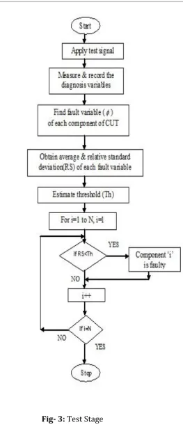
The proposed test process starts with the simulation of CUT to derive the circuit parameters and consists of two stages such as pre testing stage and testing stage. In the pre testing stage, the circuits parameters such as node voltages and currents are derived and the test vectors at the test frequencies as in (15) are generated and stored. Based on the values of test vectors the diagnosis varaiables or test variables are selected. This is shown in fig.2.
Fig-2: Pre testing stage
3.1 Selection of Diagnosis Variables or Test
Variables
© 2015, IRJET.NET- All Rights Reserved
Page 193
The testing stage consists of application of testsignal at different frequencies selected within the bandwidth of the CUT at the input node and measurement of the selected diagnosis variables. The fault variables corresponding to the components of CUT are derived from (14) and as the testing is done at multiple frequencies, the average and relative standard deviation related to the average value of the fault variables derived at each frequency is found. An average relative standard deviation value of all the fault variables is estimated and used as a threshold for identification of faulty components. A component is said to be faulty if the relative standard deviation of the fault variable corresponding to that component is less than the threshold estimated. This is explained in fig.3 and the results obtained are explained in section 4.
4. ILLUSTRATIONS
The proposed approach is validated through the simulation results of the CUT. Transistor amplifier circuit shown in fig.4 is being used as the circuit under test. The test vectors are derived from the simulation of the CUT and as in (15) and are shown in chart 1 (only for the diagnosis variables & only the magnitude). The diagnosis variables (only the magnitude) are selected based on the discussion in 3.1 and are the node voltage V5 & the
currents at the nodes 1 and 2 (I1 & I2). Transistor is
[image:4.595.288.552.81.696.2]assumed to be fault free and the device parameters are, β=150, the total input capacitance is 0.258nF. A sinusoidal signal source with 0V DC and 1V AC is used to apply the test signal at node 2 and this source coupled to the base of the transistor through a coupling capacitor of 0.2µF. Four test frequencies within the bandwidth of the amplifier are selected (50 kHz, 100 kHz, 150 kHz & 200 kHz) for testing. The components are shown with their nominal values in fig. 4.
T1
R
1
1.
26
k
R
2
18
9k
R
3
12
6k
R
4
63
0
V1 10 C1 200n
+
VG1
1
3
5 4
[image:4.595.44.548.152.753.2]2
Fig-4:
Transistor Circuit
© 2015, IRJET.NET- All Rights Reserved
Page 194
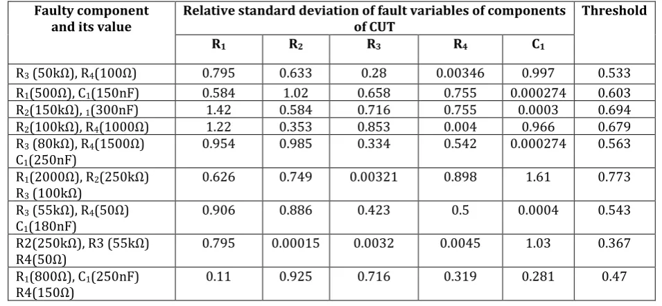
Chart - 1: Test VectorsFault detection is performed as explained in fig. 2 & fig.3. The components R1 & R2 with the faulty values 200kΩ &
100kΩ are introduced into the CUT and the fault variables are estimated at test frequencies. Average and standard deviation of the fault variables (corresponding to the components of CUT) at the test frequencies are estimated as 0.00052, 0.000152, 1.2, 0.986, 0.85 (R1,R2,R3,R4 &C1).
The threshold is the average of all these values and it is 0.609. From the values it can be identified that the
components R1 & R2 are the faulty components because
the fault variables corresponding to these components are lesser than the threshold. Results are shown in table 1 for some of the faulty conditions.
5. CONCLUSION
[image:5.595.85.563.467.688.2]A test approach based on test vectors and multiple frequency measurements is proposed to locate multiple parametric faults in nonlinear analog circuits. The diagnosis variables for testing are selected based on the test vector values without the use of specialized approaches. From the test vectors it is also possible to identify the possible components that can be detected under faulty conditions. To locate multiple faults simple thresholding technique is used. It has been found that the approach is suitable to detect maximum of three faulty conditions which is because of the threshold value chosen.
Table -1: Simulation results of Transistor amplifier circuit
Faulty component and its value
Relative standard deviation of fault variables of components of CUT
Threshold
R1 R2 R3 R4 C1
R3 (50kΩ), R4(100Ω) 0.795 0.633 0.28 0.00346 0.997 0.533
R1(500Ω), C1(150nF) 0.584 1.02 0.658 0.755 0.000274 0.603
R2(150kΩ), 1(300nF) 1.42 0.584 0.716 0.755 0.0003 0.694
R2(100kΩ), R4(1000Ω) 1.22 0.353 0.853 0.004 0.966 0.679
R3 (80kΩ), R4(1500Ω)
C1(250nF)
0.954 0.985 0.334 0.542 0.000274 0.563
R1(2000Ω), R2(250kΩ)
R3 (100kΩ)
0.626 0.749 0.00321 0.898 1.61 0.773
R3 (55kΩ), R4(50Ω)
C1(180nF)
0.906 0.886 0.423 0.5 0.0004 0.543
R2(250kΩ), R3 (55kΩ) R4(50Ω)
0.795 0.00015 0.0032 0.0045 1.03 0.367
R1(800Ω), C1(250nF)
R4(150Ω)
© 2015, IRJET.NET- All Rights Reserved
Page 195
REFERENCES
[1] G.Puvaneswari, S.UmaMaheswari, “Multiple Parametric Fault Detection based on Test Vectors and Statistical Threshold”, International Journal of Applied Engineering Research, 2015, Volume 10, No.8, pp.20485-20488
[2] Jian Sun, Chenghua Wang, Jing Sun, and Lei Wang, “Analog Circuit Soft Fault Diagnosis based on PCA and PSO-SVM”, Journal Of Networks, December 2013, Vol. 8, No. 12
[3] Yang, C., Tian, S., Long, B., Chen, F, “Methods of handling the tolerance and test-point selection problem for analog-circuit fault diagnosis”.IEEE Transactions on Instrument & Measurement, 2011,60(1), 176-185.
[4] Long B., Tian S., Wang H., “Feature vector selection method using Mahalanobis distance for diagnostics of analog circuits based on LS-SVM”, Journal of Electronic Testing: Theory and Applications. 2012; 28(5):745–755.
[5] C.-W.Ho, A.Ruehli and P.Brennan , “ The modified nodal approach to network analysis”, IEEE Transactions on Circuits and Systems, 1975, Vol.22, no.6, pp.504-509.
[6] Jiri Vilach and Kishore Singhal, Computer methods for circuit analysis and design, Van Nostrand Reinhold Company, 1983.
[7] Jose A. Soares Augusto and Carlos Beltran Almeida, “ A Tool for Single-Fault Diagnosis in Linear Analog Circuits with Tolerance Using the T-vector Approach”, Hindawi Publishing Corporation, VLSI design, 2008, pp 1-8.
[8] Adel S. Sedra, Kenneth Carless Smith, Microelectronic Circuits, Oxford University Press, 2004.
BIOGRAPHIES
Ms.G.Puvaneswari is currently
working as Assistant Professor
(Senior Grade) at Coimbatore
Institute of Technology, Coimbatore, India. She did her Bachelor’s degree in Electronics and Communication Engineering at R.M.K.Enginnering College, Madras University in April 1999 and Master’s degree in Medical Electronics at College of Engineering, Guindy, Anna University, Chennai in July 2005.
Dr.S.Uma Maheswari is presently working as an Associate Professor in the Department of Electronics and
Communication Engineering,
Coimbatore Institute of Technology, Coimbatore, India. She holds 24 years of teaching experience. Her research interests are VLSI Design, Digital Image Processing and Digital Signal Processing. She obtained her doctoral degree in Electrical and
Electronics Engineering with
specialization in Biometrics, from Bharathiar University. Coimbatore. She obtained her Masters Degree in Applied Electronics from Coimbatore Institute of Technology, March 1991 and Bachelor’s Degree in Electronics and Communication Engineering
from Government College of