J. Phys.: Condens. Matter 21 (2009) 474208 (5pp) doi:10.1088/0953-8984/21/47/474208
Using surface and interface optics to probe
the capping, with amorphous Si, of Au
atom chains grown on vicinal Si(111)
N McAlinden and J F McGilp
1School of Physics, Trinity College Dublin, Dublin 2, Republic of Ireland E-mail:[email protected]
Received 31 March 2009, in final form 16 April 2009 Published 5 November 2009
Online atstacks.iop.org/JPhysCM/21/474208
Abstract
The distinct optical signatures of aligned single and double Au atom chain structures, grown on vicinal Si(111) substrates, have been identified using reflectance anisotropy spectroscopy (RAS). Deposition of 0.04 monolayers (ML) of amorphous Si (a-Si) at room temperature perturbs the anisotropic optical response of the double chain structure. By one third of a monolayer, no significant optical anisotropy associated with the chains remains. No anisotropic response re-emerges at higher coverages, up to 4.6 nm (14.5 ML) where there is recent evidence that the crystal structure of the double chain phase is maintained under the cap. The RAS results show that the anisotropic properties of the phase are quenched by a-Si adsorption, even though the crystal structure of the capped phase appears to be preserved.
(Some figures in this article are in colour only in the electronic version)
1. Introduction
One-dimensional (1D) electronic systems are currently being intensively studied for both fundamental and technological reasons. New physical properties, such as spin–charge separation, and charge-density wave (CDW) formation due the Peierls instability can appear, while quasi-1D structures are being investigated as atomic-scale interconnects in devices. Such structures can be grown by self-assembly on Si surfaces, where the existence of an energy gap prevents the coupling of the electronic states of the nanostructure with the substrate in the vicinity of the Fermi level, allowing the quasi-1D character of the nanostructure states to be preserved [1,2].
The quasi-1D Au-induced 5 × 2 surface phase that can form on singular and vicinal Si(111) surfaces has been extensively studied by a variety of techniques [3–10]. It is generally accepted that the phase consists of metallic, double Au chains separated by a honeycomb chain of Si atoms, although the finer detail is still to be agreed [11–14]. In particular, the role of Si adatoms in stabilizing the 5 ×2 structure is still being explored [12,14,15]. Growth on vicinal surfaces has been of particular interest because Si(111), offcut
1 Author to whom any correspondence should be addressed.
by a small angle in the[¯112¯ ] direction, forms aligned, kink-free steps of considerable length on suitable heat treatment under ultra-high vacuum (UHV) conditions [16]. Offcuts in the opposite[112¯]direction also produce aligned, but generally less perfect, steps [3]. Gold chains formed on vicinal Si(111) surfaces lie parallel to the step edges, along 110, and can be hundreds of nanometers long. Also, variation of the offcut angle and direction can alter the structure and separation of the chains. For example, Si(557), which is offcut 9.5◦in the[¯112¯ ] direction, forms only single Au chains in a 5×1 structure, while Si(775), which is offcut 8.5◦in the[112¯]direction, forms only double Au chains in a 5×2 structure [9].
Recently, the capping of the Au 5×2 surface phase by a-Si has been probed using surface x-ray diffraction (SXRD) [19]. It was concluded that the 5 × 2 structural periodicity was retained under the a-Si, and that the Au atoms were located almost on the same plane. The interesting question that arises is whether the strongly anisotropic optical and electronic properties of the Au chains are significantly perturbed by the amorphous Si cap, even though the crystallographic structure is essentially retained. RAS is a sensitive probe of the Au chain structure and appears to be able to distinguish single and double chains [20]. In this paper the RAS signature of the chains is identified and RAS is then used to explore the effect of capping the Au chains using a-Si.
2. Experiment
The experiments were carried out in a UHV chamber with a base pressure below 3 × 10⁻¹¹ mbar. Auger electron
spectroscopy and low energy electron diffraction (LEED) were available for sample characterization. The Si samples were cut from n-type, phosphorous-doped wafers with a resistivity in the range 0.1–20cm. Three types of sample were used: Si(111), offcut 4◦ in the [112¯] direction, Si(775) and Si(557). The samples were degassed at 600◦C overnight, followed by flash heating to 1200◦C several times [21]. Further step alignment was achieved by depositing∼0.4 monolayer (ML) of Au from a high temperature Knudsen cell onto the sample, annealing overnight at 600◦C, and then flashing to 1200◦C to remove the Au. The pressure was kept below 5×10⁻¹⁰ mbar during
these procedures. Gold was deposited on the clean and ordered samples at various temperatures, measured with an optical pyrometer (estimated error±5◦C). Coverage was measured using a quartz crystal oscillator. The formation of the 5×2 phase was monitored in situ with RAS, with the best surface order corresponding to a maximum RAS amplitude [20]. LEED was used to confirm the surface structure. The capping layer was deposited using an a-Si sublimation source (Dr Eberl MBE-Komponenten), with the background pressure of hydrogen being kept below 2×10⁻⁹mbar.
The RAS spectrometer follows the design of Aspnes [22], but with the spectral range extended further into the infra-red (IR) region. Two magnesium fluoride polarizers, a calcium fluoride photoelectric modulator, a triple grating monochromator, and a combination of Si, InGaAs and liquid nitrogen cooled InAs detectors give a spectral range from 0.45 to 5.0 eV. In situ measurements are made using a strain-relieved fused silica window. RAS measures the difference in reflectance, at near normal incidence, of light polarized in two orthogonal directions in the surface plane of a material [22,23]. The real part of the anisotropy in the reflection coefficients normalized to the average reflection coefficient, Re[r/r], is related to the surface and bulk dielectric function components by:
Re
r r
=4πd
λ Im
ε110−ε112 εb−1
(1)
where d is the overlayer thickness, λ is the wavelength of the light, ε110 and ε112 are the surface dielectric
[image:2.595.309.549.64.243.2]function components parallel and perpendicular to the steps,
Figure 1. RAS spectra recorded after annealing at various
temperatures. Clean Si(111) ( ); room temperature deposition of 0.4 ML of Au(); after annealing at 350◦C (
•
), 400◦C(×), 425◦C(+), 440◦C (◦
); optimized deposition and annealing at 425◦C(——).respectively, and εb is the bulk dielectric function. RAS is surface and interface sensitive for a bulk isotropic (cubic) material. Due to the relatively large penetration depth of light, RAS can be used to study buried interfaces.
3. Results and discussion
Figure1shows the effect of annealing temperature on 0.4 ML of Au, corresponding to a complete 5×2 phase, deposited on 4◦offcut Si(111) at room temperature, together with the result of optimized deposition and annealing at 425◦C. The sample was held at these various temperatures for about 20 min, when no further change in the RAS response was observed. The amplitude of the anisotropic surface and interface RAS signal will, in general, be reduced by defects and disorder, and also by domain averaging. The spectral shape and the maximum amplitude in figure1were found to be reproducible and to be consistent with previous work [20]. LEED was used to confirm the formation of the 5×2 phase, but the RAS signal proved to be more useful as an indicator of surface order and quality.
The features around 3.4 and 4.25 eV, most clearly seen on the clean surface, are step-modified bulk optical transitions across the direct Si band gap [24]. Features to lower energy are related to the surface phase. The broad minimum between 1.8 and 2.8 eV shows that, in this spectral region, the dominant surface polarizability is in the direction perpendicular to the chains.
The dominant surface polarizability lies along the chains between 0.7 and 1.0 eV, as shown by the large maximum in this region in figure1. The sharpness of the onset, combined with the downturn below 0.7 eV, suggests that the structure originates from dominant interband transitions aligned along the chains, rather than the intraband transitions that can produce a Drude IR tail in metallic nanostructures [25].
Figure 2. The amplitude of the minimum at 2.2 eV plotted against
the amplitude of the maximum at 0.8 eV. The linear fit indicates that only one anisotropic structure is forming, within experimental error.
It can be seen that annealing at 425◦C is necessary to produce a well ordered surface phase, but that the combination of both deposition and annealing at 425◦C produces the best result. This is consistent with previous STM work that indicated that Si adatoms become mobile above about 250◦C [26], and that deposition at 400◦C allows the formation of the equilibrium 5×2 structure, which contains an average of one Si adatom per four unit cells [15]. Figure1shows that significant ordered regions are formed as low as 350◦C. In figure2the amplitude of the minimum at 2.2 eV is plotted against the amplitude of the maximum at 0.8 eV, using the data of figure1. The linear fit indicates that only one anisotropic ordered structure is being formed.
It has been suggested that the width of the minimum for the 4◦ offcut results from contributions from single Au chain structures that add to the predominant double chain structure of the 5×2 phase [20]. In order to explore this further, RAS measurements from Si(557)-5×1-Au and Si(775)-5×2-Au are compared in figure 3. The former has a single Au chain structure, while the latter comprises only double Au chains, as a consequence of the different offcut directions and widths of the terraces [9]. Figure 3 shows that the step-modified bulk optical transitions around 3.4 eV are similar but of opposite sign, which is an elegant confirmation of the 180◦ rotation in offcut direction between Si(775) and Si(557). The Si(557)-5 ×1-Au spectrum is consistent with previous results [20], while the new Si(775)-5×2-Au results confirm that the double Au chain structure has a distinct optical signature. Figure4 shows the result of fitting a linear combination of the single and double chain spectra (figure 3) to the 4◦ offcut results (figure 1), in the region of the minimum. A population of 32±5% single chains and 68±5% double chains gives a good fit, which begins to deviate at low energy. Figure3shows similar spectral signatures in the region of 1 eV, while figure1 is quite different and thus cannot be accommodated by the fit: this is discussed further below. These results confirm that the RAS spectral response is very sensitive to the detail of the Au chain structure.
[image:3.595.53.297.63.246.2]Figure 3. RAS spectra of Si(557)-5×1-Au ( ) and Si(775)-5×2-Au ( ).
Figure 4. The result of fitting the 4◦offcut data (+) to a linear combination of the single chain data ( ) and double chain data ( ). The fit (——) corresponds to a 32±5% single chain and 68±5% double chain contribution.
The RAS response from Ag, In and Au chains formed on Si(111) surfaces show similar minima in this spectral region [20]. Very recent ab initio density functional theory calculations of the RAS response of Si(111)-4×1-In have been successful in reproducing the narrower minimum between 1.9 and 2.4 eV observed in the RAS response of this system. The calculations reveal that both In–Si bonds and pure In chain states contribute to the signal [27]. This supports the conclusion that the different positions of the Au atoms in the single and double chain structures, with associated changes in the bonding, are the origin of the differences in the response. Figure5 shows possible structures for the single and double chains [9].
[image:3.595.316.537.288.454.2]Figure 5. Structural models for Si(557)-5×1-Au (left) and Si(775)-5×2-Au (right): the Au atoms are large light grey circles, the Si honeycomb chain atoms are small dark grey circles, and the Si adatoms are small black circles (yellow, red and black, respectively in the electronic version) (adapted from [9]).
Figure 6. Deposition of a-Si on Si(775)-5×2-Au at room temperature: 0 ML ( ), 0.04 ML (
◦
), 0.08 ML (+), 0.16 ML (×), 0.32 ML (•
), 1.00 ML ( ). Estimated error in coverage±0.02 ML.Si(775) substrates, as the kinks will terminate the Au chains more efficiently than on the 4◦ offcut. It thus appears likely that the size of the maximum between 0.7 and 1.0 eV is related to the length of the Au chains. If confirmed, this will raise interesting possibilities for the in situ monitoring of nanowire growth and, possibly, process control.
The effect of capping the double chain structure with a-Si can now be investigated. Figure6shows the Si(775)-5×2-Au RAS response, together with the effect of a-Si deposition at room temperature. Si(775) was chosen because, as mentioned above, only the double Au chain 5×2 structure is formed, which simplifies interpretation. Deposition of 0.04 ML reduces the size of the minimum by about a factor of two, while the maximum increases by a similar factor. The Si atoms do not diffuse on deposition at room temperature and thus the average population of Si adatoms per unit cell can be estimated [15]. Allowing for the error in coverage due to the thermal drift of the quartz crystal oscillator, and recalling the equilibrium population of 0.25 adatoms/unit cell, the population ranges
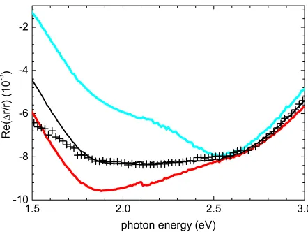
Figure 7. Higher coverages of a-Si deposited on Si(775)-5×2-Au, shown on an expanded scale: 2 ML ( ), 4 ML ( ), 6 ML ( ), 14.5 ML (4.6 nm) (——).
from about 0.5 to 0.9 Si adatoms per unit cell, for a coverage of 0.04±0.02 ML. It appears possible that the increase in the maximum is associated with the band gap opening that has been predicted to occur for a minimum energy structure with 1 adatom/unit cell [14].
By 1/3rd ML coverage the anisotropic optical response associated with the double chain structure has been quenched. At higher coverages, up to the 4.6 nm (14.5 ML) thickness used by Iwasawa et al [19], only the step-modified bulk optical transitions remain (figure 7). These features progressively reduce in size and red-shift, most likely due to the optical absorption and the strain increasing with capping layer thickness [28]. While SXRD shows that the crystal structure of the 5×2 phase is largely unchanged by capping with a-Si at room temperature [19], it is clear from these results that the technologically important anisotropic properties of the metallic chains have been destroyed.
[image:4.595.53.291.302.477.2]not affect the electronic properties of larger nanostructures significantly [18]. Quasi-1D atom chains grown by self-assembly on Si surfaces allow fascinating new physics to be explored, but capping such nanostructures with a reactive material like Si is likely to perturb the quasi-1D electronic structure. Capped phases may possess interesting and useful properties, but it will be necessary to characterize the phase beneath the capping layer to determine these.
4. Conclusion
Distinct optical signatures of aligned single and double Au atom chain structures grown on vicinal Si(111) substrates have been identified using RAS. These results offer an interesting challenge for surface ab initio optical response calculations. Deposition of small amounts of a-Si at room temperature quenches the anisotropic optical response of the double chain structure. The anisotropic response is also absent at a coverage of 4.6 nm, where SXRD has shown that the crystal structure of the buried double chain phase is largely unperturbed [19]. Nanostructures have interesting and useful properties, but capping is likely to perturb these properties where the nanostructure is only a few atomic layers in thickness. Surface and interface optical techniques offer unique advantages in characterizing such capped nanostructures.
Acknowledgments
This publication has emanated from research conducted with the financial support of Science Foundation Ireland and the Irish Research Council for Science, Engineering and Technology.
References
[1] Himpsel F J, Altmann K N, Bennewitz R, Crain J N, Kirakosian A, Lin J L and McChesney J L 2001 J. Phys.:
Condens. Matter13 11097
[2] Oncel N 2008 J. Phys.: Condens. Matter20 393001
[3] O’Mahony J D, McGilp J F, Flipse C F J, Weightman P and Leibsle F M 1994 Phys. Rev. B49 2527
[4] Collins I R, Moran J T, Andrews P T, Cosso R, Omahony J D, McGilp J F and Margaritondo G 1995 Surf. Sci.325 45
[5] Hasegawa T, Hosoki S and Yagi K 1996 Surf. Sci.355 L295
[6] Power J R, Weightman P and O’Mahony J D 1997 Phys. Rev. B
56 3587
[7] Losio R, Altmann K N and Himpsel F J 2000 Phys. Rev. Lett.
85 808
[8] Altmann K N, Crain J N, Kirakosian A, Lin J L,
Petrovykh D Y, Himpsel F J and Losio R 2001 Phys. Rev. B
64 035406
[9] Crain J N, McChesney J L, Zheng F, Gallagher M C, Snijders P C, Bissen M, Gundelach C, Erwin S C and Himpsel F J 2004 Phys. Rev. B69 125401
[10] Yoon H S, Lee J E, Park S J, Lyo I W and Kang M H 2005
Phys. Rev. B72 155443
[11] Marks L D and Plass R 1995 Phys. Rev. Lett.75 2172
[12] Erwin S C 2003 Phys. Rev. Lett.91 206101
[13] Kang M-H and Lee J Y 2003 Surf. Sci.531 1
[14] Riikonen S and Sanchez-Portal D 2005 Phys. Rev. B71 235423
[15] Kirakosian A, Crain J N, Lin J-L, McChesney J L, Petrovykh D Y, Himpsel F J and Bennewitz R 2003 Surf.
Sci.532–535 928
[16] Lin J L, Petrovykh D Y, Viernow J, Men F K, Seo D J and Himpsel F J 1998 J. Appl. Phys.84 255
[17] McGilp J F 1995 Prog. Surf. Sci.49 1
[18] Fleischer K, Jacob J, Chandola S, Esser N and McGilp J F 2008
Phys. Status Solidi c5 2556
[19] Iwasawa Y, Voegeli W, Shirasawa T, Sekiguchi K, Nojima T, Yoshida R, Takahashi T, Matsumoto M, Okano T,
Akimoto K, Kawata H and Sugiyama H 2008 Appl. Surf. Sci.
254 7803
[20] Jacob J, McAlinden N, Fleischer K, Chandola S and McGilp J F 2008 Phys. Status Solidi c5 2569
[21] O’Mahony J D, McGilp J F, Leibsle F M, Weightman P and Flipse C F J 1993 Semicond. Sci. Technol.8 495
[22] Aspnes D E 1985 J. Vac. Sci. Technol. B3 1498
[23] Weightman P, Martin D S, Cole R J and Farrell T 2005 Rep.
Prog. Phys.68 1251
[24] Yasuda T, Aspnes D E, Lee D R, Bjorkman C H and Lucovsky G 1994 J. Vac. Sci. Technol. A12 1152
[25] Fleischer K, Chandola S, Herrmann T, Esser N, Richter W and McGilp J F 2006 Phys. Rev. B74 195432
[26] Hasegawa T and Hosoki S 1996 Phys. Rev. B54 10300
[27] Wippermann S and Schmidt W G 2009 Surf. Sci.603 247
[28] Fleischer K, Carroll L, Smith C and McGilp J F 2007 J. Phys.:

![Figure 5. Structural models for Si(557)-5honeycomb chain atoms are small dark grey circles, and the Si adatoms are small black circles (yellow, red and black, respectively in theelectronic version) (adapted from [ × 1-Au (left) and Si(775)-5 × 2-Au (right): the Au atoms are large light grey circles, the Si9]).](https://thumb-us.123doks.com/thumbv2/123dok_us/8812373.919037/4.595.310.549.302.476/figure-structural-honeycomb-circles-respectively-theelectronic-version-circles.webp)
