Wirelessly Transmitting a Grayscale Image using
Visible Light
Hrushit Parikh
Dwarkadas J. Sanghvi College of Engineering, Mumbai Swami Vivekanand Road
Mumbai-400056
Jimesh Chokshi
Dwarkadas J. Sanghvi College of Engineering, Mumbai Swami Vivekanand Road
Mumbai-400056
Nimit Gala
Dwarkadas J. Sanghvi College of Engineering, Mumbai Swami Vivekanand Road
Mumbai-400056
ABSTRACT
This paper discusses the use of visible light as an alternative to wireless radio communication for short distances. The paper highlights how a regular grayscale image can be transmitted with this method and faithful reproduction is achieved at the receiver. LED bulbs are used as transmitters and the intensity of the LEDs is varied at very high rate, using OFDM modulation in accordance to the image data, such that the intensity appears constant to the human eye. Thus, apart from providing illumination, the LED bulb transmits data at high rates. Specific design measures prevent ambient light from interfering with the demodulation process at the receiver. Although this method can be currently used for short range, future developments can really expand its scope.
General Terms
Data transfer technique, visible spectrum, communication.
Keywords
Visible Light image transmission, Very high speed data transfer, OFDM, Photodiodes.
1.
INTRODUCTION
Visible light has been around us since almost the origin of the universe and will always be there. It is inherently safe, so to harness it for the purpose of communication would be phenomenal. In this paper, a model is proposed, which can be used to achieve this by taking the example of transmitting a grayscale image. In our study we realised the speeds which can be attained and this showed us the true potential of this method. Certain superior characteristics of visible light over radio waves which can be harnessed are:
Supremely high transfer speeds; theoretically of the order of 10gbps
10,000 times greater spectrum than radio waves (Radio waves correspond to a frequency band of ~300GHz to ~3 kHz, while the visible light corresponds to a frequency band of ~400 THz to ~780 THz.)
This technique has greater efficiency than radio communication. LEDs have proven operational efficiency and since visible light is used for communication, the data transfer is almost free of cost.
Commercially available PIN photodiodes are used to detect the light being transmitted. The diodes have rise and fall times ranging from a few nanoseconds to picoseconds. This corresponds to decoding rates of gigabytes per second. At the transmitter end, conventional modulation techniques can
easily match up to these rates. What is needed is error free data transmission at such high rates. This paper proposes a model which can ensure this. Image data is modulated using the high channel capacity OFDM technique and the modulated data is transmitted in the form of intensity variations of an LED bulb. Steps are taken to ensure high SNR and low bit error rate. While it is obvious that this technology will be limited by line of sight, however, it is ideal for purposes such as secure indoor communication and as a wireless access point.
2.
ENCRYPTION OF IMAGE
The format of the image does not affect the transmission in any way hence, an image of any of the regular formats- .tif; .jpeg, .bmp etc. can be selected. We are using the following .tif image having dimensions 275x183.
[image:1.595.332.541.421.563.2]
Fig 1: Image to be transmitted
We use MATLAB image processing tools to convert this image into an array and stream of binary digits corresponding to the brightness of each pixel of the image. Utilizing : X= Imread(‘image.tif’);
3.
MODULATION AND TRANSMITTER
BLOCK
3.1
Signal Representation
An OFDM signal is a sum of subcarriers that are individually modulated by phase shift keying (PSK) or quadrature amplitude modulation (QAM). [1] The symbol can be written as:
s s T
i c i
i
j
f
t
t
t
d
t
s
Ns
Ns
Ns
exp(
2
(
)(
))
,
Re
)
(
0.51 2
2
2
(1)
s(t) = 0, t<ts and t>ts + T
Ns is the number of Subcarriers
Ts is the symbol duration
[image:2.595.54.287.164.404.2]Fc is the carrier frequency
Fig. 2: Modulation and transmission. The LED is biased before applying the OFDM signal.
The binary image data to be transmitted is OFDM modulated in the following manner. The data bits and redundancy bits are demultiplexed into parallel streams, each of which is transmitted on a separate sub-carrier. Phase shift keying (PSK), and m-ary quadrature amplitude (M-QAM) modulation methods can be used [2]. The Inverse fast Fourier transform (IFFT) operation is used to modulate the sub-carriers and generate the time domain OFDM signal given as:
1
0
2
1
exp
N
n
N
n
N
k
X
j
nk
x
(2)
Where xk with k = 0, · · · ,N −1, are the N time-domain output
samples, and Xn with n =0, · · · ,N − 1, are the input symbols.
To modulate the LED intensity, the time-domain OFDM samples must be real. To ensure this complex conjugate input data symbols (e.g. Xn =X*N−n) are input to the IFFT block. A
CP (Cyclic prefix) is needed to counter the effects of multipath propagation. The CP acts as a guard interval to avoid ISI. To realize the CP, the last G samples of the OFDM symbol in eqn. (1) are repeated at the beginning so that N+G samples are transmitted. The measured channel delay spread in Optical Wireless (OW) systems is significantly less than that of RF based systems. Hence, the effect of the CP length on the bandwidth efficiency and SNR is insignificant in optical systems. [2]
Thus, in this manner the LED intensity will vary continuously in accordance to every pixel value of the image.
3.2
Fixing the Bias of LEDs and Effects of
its Non-Linearities
The digital OFDM signal is converted to its analog equivalent, amplified and this signal intensity modulates the LED as shown in Fig. 2. Since the output OFDM signal is bipolar and optical intensity cannot be negative, the LED should be biased before applying the OFDM modulating signal. This DC component is removed through a DC restoration circuit at the receiver side. At high frequencies the LED behavior is non-linear. In RF systems, the main device causing ’nonlinear’ distortions is the transmit power amplifier (PA) which is linear only over a finite range of input amplitudes. Fig. 3 provides the comparison between the two and shows the non-linearity is less prominent in Optical Systems. In optical systems, the OFDM signal envelope variations are utilized to intensity modulate the LED with its nonlinear characteristics. Selecting the correct bias point of the LED, the distortion levels can be minimized. [2] The biasing point should be carefully selected to set the maximum forward current of the LED, and to minimize magnitude distortion which is influenced by the LED operating segment of its characteristics.
4.
RECEIVER BLOCK
The first stage in the optical receiver design is the optical to electrical conversion which is shown in Fig. 4. This conversion is provided by the Photo detector (PD) and a transimpedance amplifier. The amplifier is used to amplify and convert the small PD current into a measureable voltage.
[image:2.595.317.538.409.502.2].
Fig. 3: Receiver and amplifier.
This voltage is additionally amplified and the DC component is eliminated. The signal is filtered by an anti-alias filter and then sampled by the ADC. The amplifier at the photo detector stage is absolutely necessary because the photocurrent produced by the PD is extremely small (of the order of nA) and also to convert this current into a voltage which is always easier for further processing.
[image:2.595.318.538.618.697.2]Fig. 5 shows a block diagram of the receiver. After down conversion and analog-to-digital conversion, the fast Fourier transform (FFT) is used to demodulate the N subcarriers of the OFDM signal. This happens in the signal processing block. After this process, the image data in the form of a binary bitstream is obtained.
This bitstream is then D/A converted using the same threshold used at the transmitter for A/D conversion of pixel values. This process takes place in the decryptor block. The pixel values are stored in an array of size 275x183 sequentially to reproduce the transmitted image.
5.
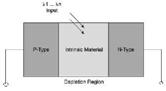
THE Si PIN PHOTODETECTOR
[image:3.595.71.240.265.357.2]PIN photodiodes can be used as Photodetectors. PIN diodes have operating wavelength range of 400-1000nm and hence, are perfect for visible light applications
Fig 5: PIN photodiode structure.
Fig 6 shows the PIN diode structure. For high speed operations, they are reverse biased. This draws current out of the central depleted region, blocking current flow unless light frees electrons and holes to carry current. The current is proportional to the amount of light absorbed which in turn increases with the thickness of the depleted region. The light absorption is concentrated in the middle intrinsic region which avoids the noise and slow response that would occur if ordinary PN photodiode was used. The typical reverse biases are 5-20V and typical response times range from a few nanoseconds to about 10 picoseconds. Sensitivity is about 0.7A/W at 800nm.
The device active area influences the detector speed and sensitivity. If the transmitting source has a cone of emission of diameter d, half-acceptance angle Ө and is at a distance S from the receiver; then it will project onto the detector a spot of diameter D [5]
D=d + 2S tan Ө (3)
Another important factor is the dark current which can introduce error in the receiver. It needs to be mitigated by proper device fabrication and in applications at room temperature it is negligible.
Avalanche Photodiodes (APDs) can be used and have faster response as they have internal gain mechanism by the process of photon multiplication which produces a veritable avalanche of carriers. Though they are extremely fast, the uneven nature of multiplication produces noise. Further, they need reverse biases of 10s-100s of volts which increases receiver complexity to the point of being impractical for our purpose.
6.
SYSTEM SNR AND ADC
RESOLUTION CONSIDERATIONS
Many sources of noise and non-linearities exist in this technology. The main source of errors is the error due to reduction in the SNR ratio due to quantization error from the ADC. It is given by [4]:
SNR = (1.763 + 6.02q) dB (4)
Where, q is the data converter bit resolution.
However, the SNR values of a practical ADC are lower than the theoretical value of (4) because of the on-chip noise such as thermal noise, and shot noise and so on. Importantly, both sources are functions of the highest frequency of the signal being sampled. Therefore, the SNR of the ADC degrades as the OFDM signal bandwidth increases. Furthermore, by taking the square root of the sum of the squares for uncorrelated noise sources, the overall system SNR can be determined using:
10 10
1
10
...
10
log
20
10k SNR SNR
system
SNR
(5)
This means that individual stage SNR figures combine so that the overall system SNR is lower than the SNR of the component with the lowest SNR. This is a serious issue which can only be addressed by choosing an ADC with an appropriate resolution based on empirical observations so as to achieve the required SNR to obtain faithful reproduction of data.
7.
EXPERIMENTAL TESTS
In the transmitter section the image was converted to a bitstream and modulated by using MATLAB code. The bits were then transmitted to an AVR by using serial communication protocols. We used a set of very basic and readily available LEDs driven by an AVR.
For the receiver section we constructed a circuit containing a PIN diode and an OPAMP amplifier. The low current from the PIN diode is amplified by the amplifier. The amplified signal is given as input to the AVR circuit which behaves as an analog to digital converter and also transmits the digital signal to the computer using serial communication protocols for demodulation and decoding. The demodulation and decoding is done by using MATLAB code.
8.
APPLICATIONS AND FUTURE
DEVELOPMENTS
The applications for this technology are limitless owing to the fact that light is probably the safest source of energy there is.
Underwater communication is an area of intensive research. Using IR and ultra-low frequency has not proved completely effective due to severe attenuation and limited bandwidth. Visible light will ultimately prove to be the optimum solution. [11] discusses the use of IrDa modulation with high power LEDs and photodiodes.
Any city street is filled with streetlamps and other sources of light. Harnessing them could provide real time information to pedestrians and street lamps could flash weather forecasts and news updates to passing vehicles. The obvious question to this would be the interference of abstract light sources. [12] addresses this issue by providing a Fourier series expression for interference. Receiver systems can be designed based on these equations. [10] goes even further to suggest the use of traffic signals to transmit traffic information.
Bluetooth transfer technology in mobile phones can be replaced with much faster and secure optical communication. Contemporary smart phones contain an LED flash. The kernel can be manipulated to modulate it and transmit data to a paired phone. One would actually see the direction of data flow. With newer generations of photodiodes getting smaller, embedding them in a mobile body will not be a task. [10] Shows the integration of a small receiver module interfaced with a port of a cell phone.
9.
LIMITATIONS
The biggest limitation at present is the limited coverage range. Even with high power LED’s practically required communication distances are not achievable. [14] presents extensive prototypes for visible light communication but still does not achieve sufficient range. Another limitation is that to implement applications, the existing infrastructure will need to be revamped. In above mentioned street light application, it is assumed that existing lighting will be replaced with high power LED sources. Although, it will prove to be beneficial in more than one way, passing such resolutions would take significant time and cost. The third limitation is to break into full-duplex mode. It would be a formidable task for a single module to transmit a modulating signal and at the same time receive and detect another modulating signal. Initial ideas include using LEDs of different wavelengths, shielding and optical isolation of transmission and receiver modules and using adaptive digital filters. Though plausible, such methods require extensive testing and research and there is barely any development on this front. Full-duplex has only been achieved by using visible light for front-end communication and using IR for back end or by morphing visible light communication with power lines. [10]
10.
CONCLUSION
The method of transmitting an image using visible light and successful reproduction has been shown, thereby, presenting a feasible method of using visible light for safe and cheap data transfer. The various steps to achieve transmission and faithful reproduction of the image have been described.
OFDM modulation is used due to great efficiency at high speeds. This method’s greatest challenge, the noise consideration, has been highlighted. The overwhelming advantages of this communication technique make this technology exciting. Though, this technology is still in its infancy, with further studies and development its far-reaching applications will only get better.
11.
ACKNOWLEDGEMENTS
We gratefully acknowledge the insight and material provided to us by our research guide Prof. Tanaji D. Biradar at every step. In addition, we acknowledge the support of the faculty members of the department of Electronics and Telecommunication, Dwarkadas J. Sanghvi College of Engineering and especially that of Prof. Dharmesh Mistry.
12.
REFERENCES
[1] A.L. Intini “Orthogonal frequency division multiplexing for wireless networks”, Graduate student UCSB, December 2000, unpublished. Retrieved from Centre for research in art technology (CREATE) website www.create.ucsb.edu.
[2] H. Elgala, R. Mesleh and H. Haas “Practical Considerations for Indoor wireless Optical System Implementation using OFDM “, downladable content from www.see.edu.ac.uk
[3] Baker. B., Microchip Technology Inc, “Article: What does the ADC SNR mean?” Retrieved from http://www.edn.com, Feb 08. [4] Jeff Hecht, Understanding fibre optics, BPB publication, second edition, Indian subcontinent, pp. 137-149.
[5] J. Kahn, J. Barry, W. Krause, M. Audeh, J. Carruthers, G. Marsh, E. Lee, and D. Messerschmitt, “High–Speed Non–Directional Infrared Communication for Wireless Local-Area Networks,” in Proc. of the 26th Asilomar Conference on Signals, Systems and Computers, vol. 1, California, USA, Oct. 26–28, 1992, pp. 83–87.
[6] Y. Tanaka, T. Komine, S. Haruyama, and M. Nakagawa, “Indoor Visible Communication Utilizing Plural White LEDs as lighting” in Proc. of the 12th IEEE International Symposium on Personal, Indoor and Mobile Radio Communications, vol. 2, San Diego, USA, Sep. 30 – Oct. 3, 2001, pp. 81–85.
[7] Mosier, R. R., and Clabaugh, R.G., “A Bandwidth Efficient Binary Transmission System”, IEEE Trans., Vol. 76, pp. 723-728 Jan 1958.
[8] Schmidl, T. M., and Cox, D.C., “Robust frequency and timing synchronization OFDM”, IEEE Trans. on Comm., Vol. 45, No. 12, pp. 1613-1621, Dec 1997.
[9] J. Grubor, S. Randel, K. Langer, and J. Walewski, “Bandwidth Efficient Indoor Optical Wireless Communications with White Light emitting Diodes,” in Proc. of the 6th International Symposium on Communication Systems, Networks and Digital Signal Processing vol. 1, Graz, Austria, Jun. 23–25, 2008, pp 165-169.
[11] Felix Schill1, Uwe R. Zimmer1, Jochen Trumpf, “Visible Spectrum Optical Communication and Distance Sensing for Underwater Applications”, proceedings of ACRA 2004.
[12] Chung Ghiu Lee “Visible Light Communication”, appears in Advanced Trends in Wireless Communications, February 2011.
[13] Wen-Yi Lin,Chia-Yi Chen, et al “0m/500Mbps WDM visible light communication systems” Optics Express, Vol. 20, Issue 9, pp. 9919-9924 (2012).
[14] Durgesh Gujjari “VISIBLE LIGHT COMMUNICATION”, August 2012, retrieved from www.dalspace.library.dal