http://dx.doi.org/10.4236/ajac.2014.54030
On-Chip Capillary Electrophoresis
(Chip-CE) with Optical On-Chip
Leaky-Waveguide-Based Detection
Christoph Doering, Matthias Grewe, Ingo Steingoetter, Henning Fouckhardt
Integrated Optoelectronics and Microoptics Research Group, Physics Department, Kaiserslautern University of Technology, Kaiserslautern, Germany
Email: [email protected]
Received 20 January 2014; revised 25 February 2014; accepted 5 March 2014
Copyright © 2014 by authors and Scientific Research Publishing Inc.
This work is licensed under the Creative Commons Attribution International License (CC BY).
http://creativecommons.org/licenses/by/4.0/
Abstract
Capillary electrophoresis (CE) suffers from a relatively small sensitivity—at least in case of optical detection transversely to the capillary axis due to the small capillary inner diameters in the range of 50 - 100 µm. Different concepts like bubble, U-, or Z-cells have been used to tackle that problem already in the nineties of the last century. But the U- and Z-cells have typically been extra cells with larger inner channel diameters and no optimization for optical waveguiding and the bubble cell per se did not allow for optical waveguiding. In the case of on-chip capillary electrophoresis (chip-CE) a U-cell can be implemented quite easily on the chip. Here we show how leaky optical waveguiding can be employed to improve optical detection. Proper U-channel design and prepa-ration by wet-chemical etching of the fused silica sub- and superstrate, making the U-channel bend a part of the optical input lens system, can help to achieve high coupling efficiency with loss coeffi-cients around 2 dB and low waveguiding loss.
Keywords
On-Chip Capillary Electrophoresis; Optical Aetection; Leaky Waveguides
1. Introduction
by total internal reflection, where the main portion of the light field is propagating within an area of high refrac-tive index—like 1.47 for fused silica. In this case the often aqueous analyte solution with a refracrefrac-tive index around 1.33 can only serve as a waveguide cladding with an evanescent field.
Therefore, leaky waveguiding is an option [10]-[16], where the waveguide core is free to have any refractive index and transverse layers or regions act as coupled transverse optical resonators for grazing light incidence, redirecting the field into the core, as depicted in Figure 1. The notion “leaky waveguide” stems from that part of the light power not redirected, causing unavoidable loss. For acceptably low loss waveguiding distances are li-mited to centi- or even millimeters. But for inner capillary diameters of 50 - 100 µm the transverse resonators and their production expenditures are not even necessary [17]; the Fresnel reflections at the single interface bet-ween the fluid and the fused silica wall suffice to achieve acceptably low waveguiding loss.
In [17] we also showed exemplarily for hyper Rayleigh scattering (HRS [18] [19])—and a planar chip with fused silica substrate and superstrate—that this concept can enhance detection efficiency by at least a factor of 20. This is due to the long path of high pump intensity along the channel waveguide then with a length of 15 mm and due to the low reabsorption of the HRS light on its short way transversely out of the then 100 µm broad channel—Here we extend this leaky waveguide approach by showing that the round cross-section wet-chemi- cally etched into the fused silica substrate/superstrate can work as a dispersing lens at the waveguide bend. This lens and an external lens system are jointly optimized to improve optical input efficiency.
2. Chip
2.1. Design
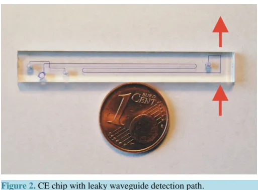
The complete planar CE-Chip is shown in Figure 2 with a size comparison to a Euro cent coin (16 mm coin diameter). The optical path is marked by the arrows in Figure 2.
2.2. Technology
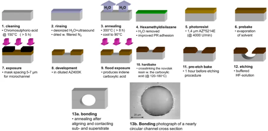
Figure 3 gives an overview of the technological process to realize the chip by wet-etching both the substrate and the superstrate in the same way with mirror-inverted channel patterns. First both have to be thoroughly cleaned and prepared for photoresist wetting. Then both are spin-coated with the photoresist; different resist options are possible [17] [20] [21]. Then the latter is exposed to ultraviolet light in the pattern of the channel lay-out, de-veloped, and hardbaked. The opening in the photoresist layer allows for wet-chemical etching of the substrate and superstrate by buffered hydrofluoric acid. The wet-etching causes half-round cross-sections (giving half-cy- lindrical channels). After photoresist descum in an oxygen plasma the fluid inlet holes have to be drilled or sand-blasted. Then sub- and superstrate are aligned and bonded by pressure and heat treatment with severe alignment tolerances of less than 1 µm [22]. At the bottom of Figure 3 a microscope image of a channel cross- section after bonding of sub- and superstrate is shown; as intended no optical interface between both chip halves can be observed. (Note that in this case the chip has only been transversely sawed to make the microscope image of Figure 3 possible.)
Figure 1. Illustration of leaky optical waveguiding; r is the radial co- ordinate, n denotes the refractive index.
Figure 2. CE chip with leaky waveguide detection path.
the case of a Galilei-type telescope. (Note, that these microscope images show a slightly other chip version with an oblique feeding capillary as opposed to the case in Figure 2.) For the micrograph on the right in Figure 4 the capillary has been completely filled by the dye/chromophore Rhodamine 6G and illuminated/excited from out-side with the light of an Ar+ laser. The fluorescence extends over the whole straight channel, because the excit-ing beam is guided in this channel.
For a channel diameter of ≈65 µm and the optimized optical system, the results averaged over typical solvents (like water, methanol, and dioxane) and over the wavelengths of the visible spectrum, the waveguide insertion loss is about 2.0 dB for optical input (and output) coupling and about 0.07 dB/mm due to the leaky character of the optical waveguiding, i.e. f.e. 0.70 dB for a 10 mm long waveguide section, giving a loss of about 2.70 dB altogether [17] [22].
4. CE Fluorescence Detection
Figure 3. Sketch of technological process for CE-chip realization. Other photoresist (PR) options are possible.
Figure 4. Channel bend with optical function as a dispersing lens forming a lens system with the external achromatic lens set-up, i.e. a Galilei-type telescope. On the right fluorescence of a Rhodamine 6G dye solution—here fully filling the channel— excited by Ar+ laser light can be observed. The inner channel diameter is about 65 µm here.
The CE result is shown in Figure 5. Two fluorescence peaks demonstrate a temporal and spatial separation of the two markers Rhodamine and Fluorescein. The Rhodamine plug reaches the position of the fiber tip for detec-tion first—after 85 s. The maximum of its fluorescence signal is at a wavelength of 566 nm. About 60 s later the Fluorescein plug reaches the detection fiber. Here the fluorescence maximum is at 547 nm.
5. Conclusions
[image:4.595.194.433.337.550.2]Figure 5. CE separation result for the chromophores Rhoda- mine B (R B) and Fluorescein 27 (F 27). The fluorescence maximum for R B is at a wavelength of 566 nm, while that for F 27 is at 547 nm. The retention time for R B is 85 s, while that for F 27 is 145 s.
—exemplarily for the excitation light in fluorescence detection. Efficient input coupling can be achieved by in-corporation of a wet-chemically etched waveguide bend. It acts as a dispersing lens and forms a Galilei-type telescope together with an external achromatic lens set-up.
In principle, the waveguiding concept can also be employed for other types of separation techniques and other methods of optical detection, like absorption spectroscopy. In the latter case f.e. the waveguided light can be coupled out of the channel again in the longitudinal direction with another Galilei-type micro telescope.
Acknowledgements
The work was financially supported by the German Research Foundation (DFG, Deutsche Forschungsgemein-schaft) under contract FO157/15.
References
[1] Hewlett-Packard (Now Agilent Technologies) (1992) Product Specifications on Capillaries with Bubble Cell.
[2] Kaltenbach, P. (1995) A High-Sensitivity Diode Array Detector for On-Column Detection in Capillary Electrophoresis.
HP Journal, 46, 20-24.
[3] Agilent Technologies (1997) Agilent Technologies Technical Note. 5965-5984.
[4] Bruno, A.E., Gassmann, E., Pericles, N. and Anton, K. (1989) On-Column Capillary Flow Cell Utilizing Optical Wa- veguide for Chromatographic Applications. Analytical Chemistry, 61, 876-883.
[5] Verpoorte, E., Manz, A., Luedi, H., Widmer, H.M., van der Schoot, B.H. and de Rooij, N.F. (1991) A Novel Optical Detector Cell for Use in Miniaturized Total Chemical Analysis Systems. Proceedings of the International Conference on Solid-State Sensors and Actuators, San Francisco, 24-27 June 1991, 796-799.
[6] Verpoorte, E., Manz, A., Luedi, H., Bruno, A.E., Maystre, F., Krattiger, B., Widmer, H.M., van der Schoot, B.H. and de Rooij, N.F. (1992) A Silicon Flow Cell for Optical Detection in Miniaturized Total Chemical Analysis Systems.
Sensors and Actuators B Chemical, 6, 66-70. http://dx.doi.org/10.1016/0925-4005(92)80032-S
[7] Moring, S.E., Reel, R.T. and van Soest, R.E.J. (1992) Optical Improvements of a Z Shaped Cell for High-Sensitivity UV Absorbance Detection in Capillary Electrophoresis. Analytical Chemistry, 65, 3454-3459.
http://dx.doi.org/10.1021/ac00071a020
[8] Tiefenthaler, K. and Lukosz, W. (1984) Integrated Optical Switches and Gas Sensors. Optics Letters, 9, 137-139. http://dx.doi.org/10.1364/OL.9.000137
[image:5.595.205.416.84.270.2][15] Fouckhardt, H. and Delonge, T. (1996) Optical Detector Including Bragg Waveguide Structure. US Patent Nr. 5572328.
[16] Fouckhardt, H. and Delonge, T. (1997) An Optical Detector Device. European Patent Nr. EP 0 679 881 B1.
[17] Fouckhardt, H., Grosse, A., Grewe, M. and Kuhnke, M. (2001) Micro Flow Modules with Combined Fluid Flow Chan- nel and Optical Detection Waveguide—Hyper Rayleigh Scattering as a Case Study. Fresenius Journal of Analytical Chemistry, 371, 218-227. http://dx.doi.org/10.1007/s002160100963
[18] Stadler, S., Braeuchle, C., Brandl, S. and Gompper, R. (1996) Experimental Determination of the First Hyperpolariza- bility of New Chiral and Achiral Octupolar Tertiary Amines by Hyper-Rayleigh Scattering. Chemistry of Materials, 8, 414-417. http://dx.doi.org/10.1021/cm9503487
[19] Stadler, S., Braeuchle, C., Brandl, S. and Gompper, R. (1996) Determination of the First Hyperpolarizabilities of Oc- tupolar Molecular Ions Made from Symmetric Cyanine Dyes. Chemistry of Materials, 8, 676-678.
http://dx.doi.org/10.1021/cm950453g
[20] Steingötter, I. and Fouckhardt, H. (2005) Deep Fused Silica Wet Etching Using an Au-Free and Stress Reduced Sputter Deposited Cr Hard Mask. Journal of Micromechanics and Microengeering, 15, 2130-2135.
http://dx.doi.org/10.1088/0960-1317/15/11/019
[21] Kimmle, C., Wolff, S., Doering, C. and Fouckhardt, H. (2013) Dependence of Fused-Silica Etch Rate on the Etch Mask Opening Diameter. Microelectronic Engineering, 112, 10-13. http://dx.doi.org/10.1016/j.mee.2013.05.006 [22] Grosse, A., Grewe, M. and Fouckhardt, H. (2001) Deep Wet Etching of Fused Silica Glass for Hollow Capillary Opti-